Author: admin

  • The Impact Of AI On Semiconductor Manufacturing

    The Impact Of AI On Semiconductor Manufacturing

    Photo by DeepMind on Unsplash


    Artificial Intelligence (AI) plays an increasingly important role in semiconductor fabrication. AI is being used to automate the semiconductor process of designing and manufacturing semiconductors and optimize the process for maximum efficiency.

    Additionally, AI detects and diagnoses problems in the fabrication process, allowing for faster resolution. However, deploying AI in this sector comes with a price. Irrespective, AI can help reduce overall operational costs, increase productivity, and improve product quality.

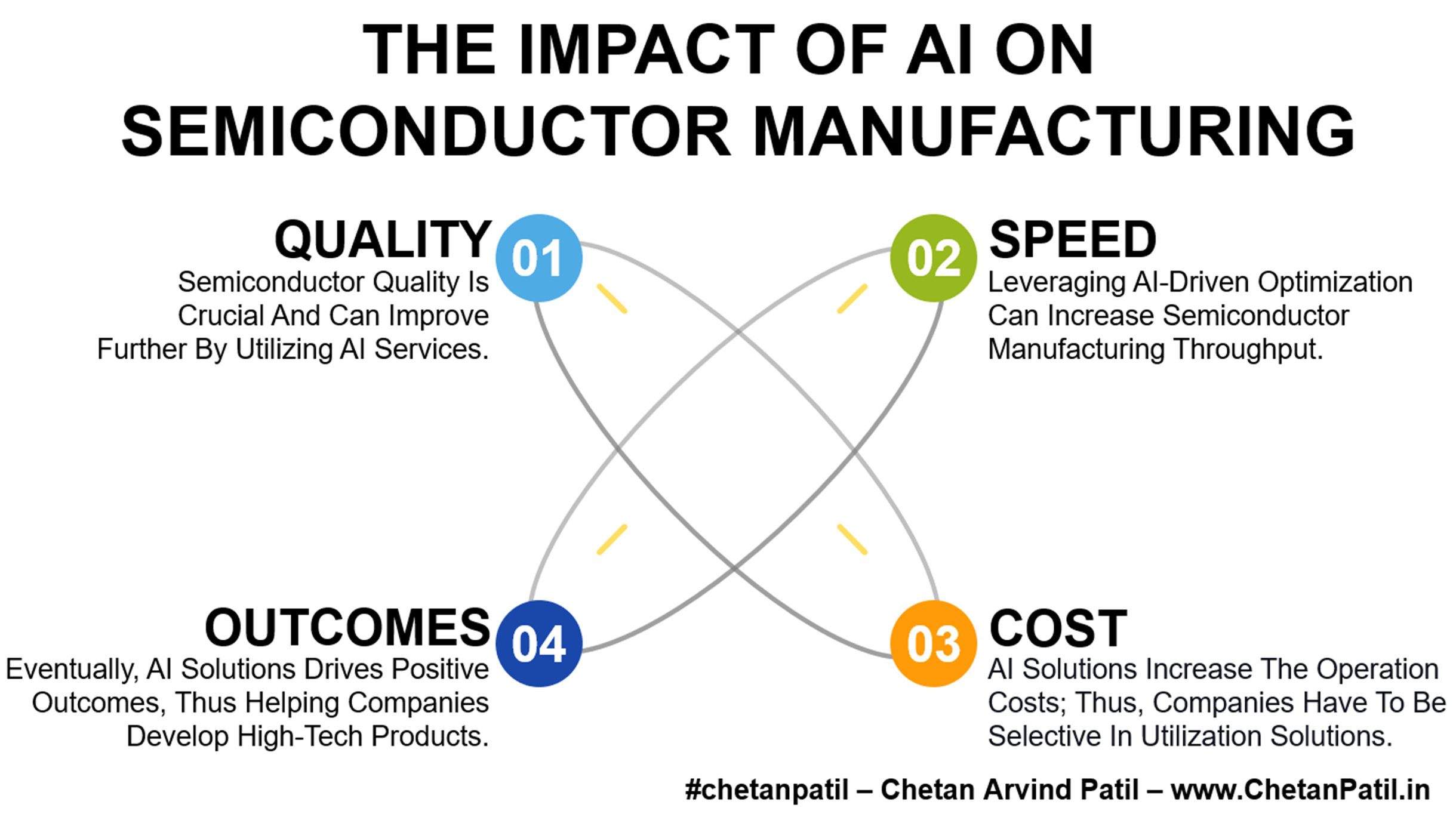
    Quality: Semiconductor Quality Is Crucial And Can Improve Further By Utilizing AI Services.

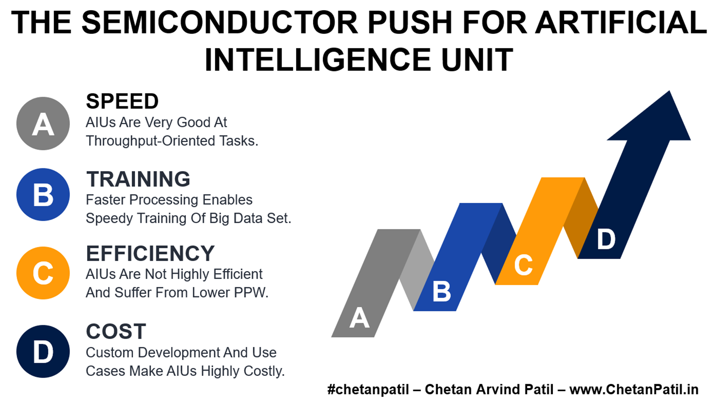
    Speed: Leveraging AI-Driven Optimization Can Increase Semiconductor Manufacturing Throughput.

    AI-driven automation can also help streamline the manufacturing process from design to delivery by analyzing the fabrication process data, identifying defects, and optimizing procedures. AI can automate several aspects of the fabrication process, allowing for faster production times and improved quality control.

    However, deploying AI in semiconductor manufacturing can take time and effort. It requires significant resources to develop AI applications’ algorithms, hardware, and software. On top, the cost of training and maintaining the AI system is also high.


    Picture By Chetan Arvind Patil

    Several factors drive the cost of AI in semiconductor manufacturing. Such as the complexity of the application, the size of data sets used for training, and the number of resources required to maintain it. Furthermore, additional costs are associated with integrating existing systems with new AI solutions. These factors increase the cost of deploying AI in the semiconductor industry.

    Nevertheless, the future of AI in a semiconductor is encouraging. With the help of AI, semiconductor companies can develop more efficient and cost-effective solutions for their customers. Several design and manufacturing process steps currently rely on AI solutions to speed up analysis and thus help speedy production output.

    Cost: AI Solutions Increase The Operation Costs; Thus, Companies Have To Be Selective In Utilization Solutions.

    Outcomes: Eventually, AI Solutions Drives Positive Outcomes, Thus Helping Companies Develop High-Tech Products.

    One of the better use cases of AI in semiconductor manufacturing is to predict future trends in the industry, which can help develop new products and services tailored to market needs. As a result, semiconductor companies will be able to stay competitive in the market and provide better products and services for their customers.

    AI is revolutionizing the semiconductor industry by providing a range of benefits. AI-enabled semiconductors can perform complex tasks with greater accuracy and speed than ever before. With all such advantages, it is no wonder that AI is becoming an increasingly important part of the semiconductor industry.


  • The Semiconductor Capacity Expansion Flow

    The Semiconductor Capacity Expansion Flow

    Photo by frank mckenna on Unsplash


    Semiconductor capacity is a critical factor in the future of the electronics industry. Thus, it is essential to ensure a balance between the demand and supply of semiconductors, as well as cost-effectiveness and capital expenditure (CapEx).

    Also, the semiconductor industry has seen tremendous growth recently, with the demand for chips increasing significantly. It has increased CapEx for semiconductor manufacturers as they strive to meet the growing demand. However, this increased spending has also resulted in higher costs for consumers.

    Capacity: The Capacity Of Semiconductor Manufacturing Is Critical In Meeting The Required Demand.

    Customer: Managing Capacity Is Crucial In Meeting Customer Deadlines.

    Thus, companies must manage their semiconductor capacity effectively to remain competitive and profitable. It means understanding the current market conditions and predicting future trends so that they can plan accordingly.

    On another side, investing in the latest technology node is also essential for companies to stay competitive in the semiconductor industry. The technology node refers to the size of a chip measured in nanometers and directly impacts performance and data processing capabilities. As such, companies are investing in new technology nodes that can give them an edge over their competitors.


    Picture By Chetan Arvind Patil

    The cost of investing in new technology nodes can be high, but the potential benefits are significant. Semiconductor companies must carefully consider their investment strategy before investing in a new technology node. Otherwise, the long-term negative impact can derail companies from their stronghold and put them behind in the market.

    The semiconductor supply chain is a complex system that requires careful management to ensure cost-effectiveness and reliability. With the increasing demand for semiconductors, it is becoming increasingly important to accurately predict future shortages and manage the data associated with the supply chain.

    Balance: Balancing Semiconductor Capacity Requires Capturing Different Supply And Demand Data Points.

    Future: Semiconductor Manufacturers Need To Predict And Manage Future Capacity To Avoid Shortages.

    Semiconductor capacity planning is a critical process for the success of any semiconductor manufacturing business. It involves carefully considering factors such as OSAT, FAB, wafer cost, assembly and testing process flow, and other related costs. By understanding these factors and their impact on the production process, companies can make informed decisions about optimizing their production capacity. It will help them to maximize efficiency while minimizing costs.

    The semiconductor industry is one of the world’s most dynamic and rapidly changing industries. As technology advances, so makes the demand for semiconductors, and to meet all this demand, it will be crucial to plan the manufacturing capacity correctly and invest and develop resources today.


  • The Semiconductor And Sports

    The Semiconductor And Sports

    Photo by Javier Miranda on Unsplash


    The use of semiconductor technology in sports is becoming increasingly popular. With the help of data collected from sensors, athletes can now track their performance and improve their game. This data also allows coaches to make better decisions.

    Semiconductor technology has also enabled sports fans to get closer to live action. Through virtual reality-like technology, fans can experience a game as if they were there. A mix of such and other semiconductor-driven technology has also allowed more accurate predictions and analysis of games, giving fans an even greater insight into the sport they follow.

    Use-Case: Sports Industry Has Speedily Adopted Technology.

    Insights: Adoption Of Technology Now Provides Better Data-Driven Insights.

    For sports, semiconductor products improve performance while reducing injury risk by providing data-driven insights into how athletes can best optimize their training and game strategies. With the help of semiconductor-powered devices, sports teams can now make more informed decisions about how they train and compete.

    For example, silicon-powered products in sports like football, tennis, and racing are in use. Football teams use them to track player performance and analyze data from games. Tennis players use them to measure their swing speed and accuracy. And race car drivers rely on them to monitor engine performance and optimize driving strategies. All such use cases have created a niche market for semiconductor companies.


    Picture By Chetan Arvind Patil

    Technology will continue to play an essential role in the world of sports. Semiconductors are at the heart of this transformation. To continue to support such a transition, companies will also have to focus on creating silicon chips geared towards enabling end-products that can bring sports and athletes closer than ever before.

    Semiconductor technology has enabled a range of new applications in the sports industry, from wearables that track performance data to virtual reality experiences that allow fans to experience games from home. As this technology continues to evolve, it will open up even more business opportunities in sports and the semiconductor industry.

    Performance: All This Is Possible Due To The Use Of Highly Accurate Semiconductor Devices.

    Impact: Sports Technology Has Opened Up New Avenue For Semiconductor Industry.

    The sports industry is a rapidly growing sector, with the global market size estimated to reach $717.4 billion by 2027. This growth is also driving the demand for semiconductor technology to cater to different types of products that can drive sports and enable global connectivity.

    The market size for semiconductors in sports will grow significantly over the next few years. This growth is due to the demand for data-driven insights and analytics that help teams make better decisions on and off the field. Additionally, technological advances, such as 5G, will enable faster data transfer speeds, enhancing the semiconductor’s impact on sports. As more teams adopt these technologies, it’s clear that semiconductors will significantly impact how we experience sports in the future.


  • The AI Semiconductor Stack

    The AI Semiconductor Stack

    Photo by Jelleke Vanooteghem on Unsplash


    The use cases of Artificial Intelligence are increasing year after year. To deliver the much-required performance, the silicon technology platform is critical. The computing industry has developed different types of AI-inspired applications and is now looking for a perfect silicon architecture that can cater to different application scenarios.

    In this process, the semiconductor industry has provided the silicon platforms like GPUs, TPUs, NPUs, and AIUs. The common trait across these silicon platforms has been the internals on how different data processing occurs. Eventually, the AI applications require high throughput to ensure the time taken to perform inference and training is the smallest possible.

    Memory Management: AI Semiconductor Stack Demands Speedy And Error-Free Data Movement Via Memory Stacks.

    Data Storage: Enabling On-The-Go Analysis Requires Silicon AI Semiconductor Stack That Can Provide Ample Amount Of Data Storage.

    The internals of AI Stack for semiconductor solutions requires near-perfect memory management. The key to handling a large data set is memory. The silicon architecture has to ensure that the AI application is not running into memory bottlenecks. If they do, the silicon architecture will slow down the AI application and eventually harms the customer experience.

    Silicon architecture also has to ensure that data management is not a bottleneck. It requires an interaction between the upper-level memories (caches) with the lower-level (disk)memories. The penalty of slow processing across these two levels is on processing time, which is a critical component of AI applications.


    Picture By Chetan Arvind Patil

    As the application of AI grows further, the computing power will have to also increase with it. Thus, on top of the memory management and data movement, the two other critical components are data logic and network-on-a-chip.

    Data logic ensures the processing aspect is error-free, thus no bottlenecks when interacting with different sub-blocks. It is a critical requirement of high-performance processors and an area that academic and industry researchers have continuously worked to enhance.

    Data Logic: Underlying Data Pipeline Needs Logic Blocks That Can Ensure There Are No Processing Bottlenecks.

    Network Of Chips: Single Die Is Not Doing To Work For AI Semiconductor Stack. It Is Where Networks Of Multi-Die Is Needed.

    Apart from all the technical considerations, the last part of the AI Semiconductor Stack is cost. Eventually, the silicon solution deployed to handle the AI applications should be cost-friendly. It means the cost of processing per bit does not negatively impact the business side of the AI use case.

    The computing industry will keep launching novel uses cases for AI applications. Today, it is ChatGPT. Tomorrow it will be something else. Eventually, the underlying silicon architecture will have to cater to all the changing requirements and thus will have to ensure all the AI Semiconductor Stacks are technically robust and business-wise budget-friendly.


  • The Semiconductor Push For Artificial Intelligence Unit

    The Semiconductor Push For Artificial Intelligence Unit

    Photo by DeepMind on Unsplash


    System-On-A-Chip (SoC) has been in the market for decades. The core-level features have provided the much-needed processing capabilities to drive data-driven applications.

    However, the capabilities provided by the underlying architecture of SoC are not suitable for applications that are always crunching and training the data. For such applications, a faster processing capability is a must. Which the traditional SoCs are not capable of providing.

    Speed: AIUs Are Very Good At Throughput-Oriented Tasks.

    Training: Faster Processing Enables Speedy Training Of Big Data Set.

    It is where a new set of computer architecture comes into play. These are Artificial Intelligence Units (AIUs), which cater to the training demand of new-age applications. Given the purpose of AIUs is data throughput, the inference and training part of the data engineering is highly efficient compared to the traditional CPUs.

    The core reason for such high efficiency of training is math operations. AIUs can provide the required architecture and memory organization that makes the math operation near-bottleneck-free compared to any other processing unit.


    Picture By Chetan Arvind Patil

    AIUs architectures can reduce the time to train a data set drastically. At the same time, the power requirement (at the gain of performance) makes them inefficient. This efficiency is due to the power and cooling needs.

    Not just AIUs, the widely used GPUs (for data training) face this issue. So far, the semiconductor industry has not been able to derive a long-term solution to ensure that complex architectures like GPUs and AIUs are low-power while not compromising performance.

    Efficiency: AIUs Are Not Highly Efficient And Suffer From Lower PPW.

    Cost: Custom Development And Use Cases Make AIUs Highly Costly.

    AIUs are for highly specialized and specific tasks. Thus, the use case of AIUs is very niche and not a mass-market solution. The impact of such use cases is on the cost. It also raises questions on how long AIUs can be relevant if the use cases are limited.

    Nevertheless, the semiconductor industry cannot rely on traditional cores to process adaptive applications. Thus, developing solutions like AIUs is the correct course of action, and now it is up to the computing industry to make the most of such solutions.


  • Chipmakers’ Bold Strategy For Revenue Spike: Foray Into The Services Industry

    Published By: Analytics India Magazine
    Date: 6th January 2023
    Media Type: Online Media Website

  • The Semiconductor Puzzle To Build End Products

    The Semiconductor Puzzle To Build End Products

    Photo by Oleg Gospodarec on Unsplash


    There are thousands of different types of semiconductor chips in the market. Year after year, the number is only increasing. Thus, creating a large pool of options to choose from while also enabling customers with different feature sets.

    Ideally, this should be positive news for companies using semiconductor chips to build end products. However, such an increase in options is also creating a situation where it is slowly becoming difficult to narrow down the specific types of chips one should use to build the end products for the mass market.

    Application: Application Requirement Are Key To Building The Right End Product Using Semiconductor Chips.

    Feature: Listing Down Features Is A Better Approach To Narrow On Specific Semiconductor Chips To Use.

    Take an example of an integrated circuit with logic devices. At any given point, there are close to 90,000 different options. The same is the case with power management integrated circuits, where the number grows to 300,000. Searching for the correct semiconductor chips from a large set of options (that too, two of the several other semiconductor segments) is nothing less than finding a needle in a haystack.

    Is there a way to solve this problem and thus enable faster decision-making? In reality, there is no better approach to tackle such a problem. Nevertheless, companies can opt for a step-by-step approach to narrow down specific types of chips that will help build the envisioned end products, and this requires immense focus on the selection process.


    Picture By Chetan Arvind Patil

    There are sets of processes that can help in faster decisions on selecting silicon chips. However, the fundamental approach should always include a detailed analysis of the target application, as it allows companies to focus on specific types of chips to narrow on.

    As a next step, based on the list narrowed as per the application type, the focus should shift to the features. If the same chip can provide different features per application type, it should be preferred rather than opting for several chips.

    Search: Searching Through Thousands Of Different Types Of Options Is A Time And Cost-Intensive Process.

    Product: Building A Product With Semiconductor Chips Is All About Finding The Right Set Of Different Types Of Chips.

    Finding a perfect match of features based on the target application solves more than half of the puzzle to build next-gen end products. In the future, such a process will be far easier when AI-enabled software tools drive efficient searches to help system engineers come to a decision faster than ever.

    As the semiconductor industry marches ahead of trillion devices, the chip selection process for the end product will become more vital than ever. It will also define the flow for manufacturing future next-gen silicon-driven end products.


  • The Call To Balance The Semiconductor Nodes

    The Call To Balance The Semiconductor Nodes

    Photo by Maxence Pira on Unsplash


    The semiconductor node is the most vital technical topic in the semiconductor industry. Technology node forms the basis for developing different types of silicon products. Over the last decade, top semiconductor manufacturers have invested a lot of time and capital to bring new semiconductor technology nodes.

    Such push is due to two critical aspects. The first one is technical, as it focuses on bringing new advanced solutions to the market. The second one is more business-oriented, where the manufacturers bring new capacity to manage future demand.

    Focus: Semiconductor Companies Consistently Focus On New Node Technology.

    Planning: Semiconductor Node Development Demands Capacity Planning.

    Eventually, the demand for a specific technology node is due to the market and application use cases. However, even with all the available data about how the consumer market will grow, there is still a gap between the type of technology node capacity.

    This gap is due to the focus on bringing capacity for the matured technology. It is a logical step given the need to cater to different system applications that still rely on such technology nodes. On the other side, to ensure future demand for advanced nodes is met, there needs to be a balance in semiconductor fabrication capacity.


    Picture By Chetan Arvind Patil

    To bring the balance in semiconductor technology nodes, not only manufacturers should plan and invest, but public bodies also need to provide the required incentives and policies impetus. Several of the advanced semiconductor node FABs are only possible due to support from government bodies.

    The current view of semiconductor FAB type clearly shows that the 200nm wafer FABs are dominant. Within 200nm FABs, matured technology capacity share is more than 30-40%. It is due to the market requirements and the need to support legacy products.

    Balance: A Perfect Balance Of Technical And Business Requirements Is Needed.

    Application: Semiconductor Application And Use Cases Are Changing The Node Roadmap.

    However, long term, the share should reduce from matured to advanced technology, mainly to ensure the next-gen applications can use the features provided by the advanced technology node.

    As the focus on building better and larger semiconductor FABs increases, the crucial part will be to plan the capacity concerning the node type. So that it not only benefits future applications but also pushes the semiconductor industry towards shortage resiliency.


  • The Global Shift In Semiconductor Ecosystem

    The Global Shift In Semiconductor Ecosystem

    Photo by Maxence Pira on Unsplash


    The semiconductor ecosystem comprises distributed end-to-end semiconductor processes. These processes cover a different aspects of silicon development. It ranges from the market requirement, then moves to design, validation and if all goes as planned, then eventually mass manufacturing.

    However, these steps are not guaranteed to be performed by a specific location or region. It is where the semiconductor ecosystem comes into the picture.

    Global: Semiconductor Industry Is Adopting To The Changing Global Scenarios.

    Shift: Different Types Of Government Policies Are Shifting The Semiconductor Industry Process.

    In semiconductors, product development is dependent on different parts of the world. Given the recent shift in investment, planning, policies, and talent, this ecosystem is going through a tectonic shift that will have positive and negative consequences on future semiconductor technologies.

    On the positive side, such a shift is bringing better equilibrium in terms of investment, and also technological development is getting more distributed.


    Picture By Chetan Arvind Patil

    On the negative side, it has created technology-driven conflicts between different regions. Eventually, a middle way will have to be carved, where both the new and existing will grow and contribute to the semiconductor industry.

    Based on past, current, and future scenarios, the semiconductor industry will always be global. As such, any shift should not let a specific region dominate the end-to-end semiconductor processes.

    Conflict: Conflicts Between Different Regions Is Creating A Tectonic Shift In Semiconductor Business.

    Ecosystem: All The Geo Changes Are Leading To A New Type Of Semiconductor Ecosystem.

    A connected, dependent, global and decentralized approach is the primary reason the semiconductor industry will keep growing at a double-digit. Changing such an ecosystem is not an easy process. It is also about time different countries work together to enable next-gen solutions for ever demanding and ever-growing semiconductor market.

    The next few years will bring a lot of conflicts for the semiconductor industry and will challenge the traditional notion of how distributed and region dependent the semiconductor ecosystem is. Eventually, the semiconductor industry will have to balance by focusing on the next-gen advancement, which will have to be driven by the distributed semiconductor ecosystem, and no one region should dominate.


  • The Constant Rise Of Semiconductor FPGA

    Photo by Maxence Pira on Unsplash


    Adaptive, specialized, and the balance of power and performance have become a central point for designing different types of efficient processing units. To help with this vision, FPGAs have become an integral part. Mainly due to the features FPGA architecture provides.

    Currently, the market size of FPGA is approximately ten billion dollars. As the demand for real-time adaptive silicon increases, this market will grow tenfold. All this is opening up opportunities for XPU-focused semiconductor companies to leverage the FPGA-demanding market.

    Flexibility: FPGA Brings Flexibility To The Processing Units.

    Assistance: Drives New Ways To Process Compute And Memory Intensive Workloads.

    FPGAs are accompanying devices that reside next to the core processing unit and thus processing. It enables offloading features that provide flexibility XPUs in load balancing.

    It is the main reason several performance-oriented XPUs today get equipped with embeddable FPGA, which allows on-the-go training/testing of the learning algorithm. A feature that is also pushing the boundaries of machine learning.


    Picture By Chetan Arvind Patil

    FPGAs are also enabling semiconductor companies to focus on new types of applications. Several of these have inspired new-age computing-dependent industries like agro-tech, robotics, space tech, and several others.

    All this is because of the FPGA design features, which are highly adaptive as it provides the ability to deploy FPGA as per the target application requirements. FPGA architectural features are getting used in designing new-age modular XPU designs that have opened up new ways to deploy applications.

    Application: FPGAs Provide Ability To Expand System Level Applications.

    Design: New Design Methodology That Provides More Options To The Customers.

    Even though there are several benefits of FPGA, there is one big hurdle that FPGA brings. It is the manufacturability. FPGA is very complex by design, and embedding them with any other XPU makes the semiconductor manufacturing process harder and raises yield concerns.

    Several semiconductor companies have acquired the design and manufacturing knowledge to make their XPUs more FPGA friendly. All this will help the semiconductor industry to develop advanced XPUs that will drive computing to new levels.