Author: admin

  • The Dilemma Between General Purpose And Domain Specific Semiconductor Solutions

    The Dilemma Between General Purpose And Domain Specific Semiconductor Solutions

    Photo by Robert Ruggiero on Unsplash


    The development of new technology always leads to new types of data. Processing varying and vast amounts of data require computer architecture. These architectures balance the latency and throughput to ensure the user experience is not compromised. And to enhance the user experience, the computing industry has been switching between general purpose and domain-specific architectures. However, for future workloads, it has now created a dilemma on which of these two solutions will be dominant.

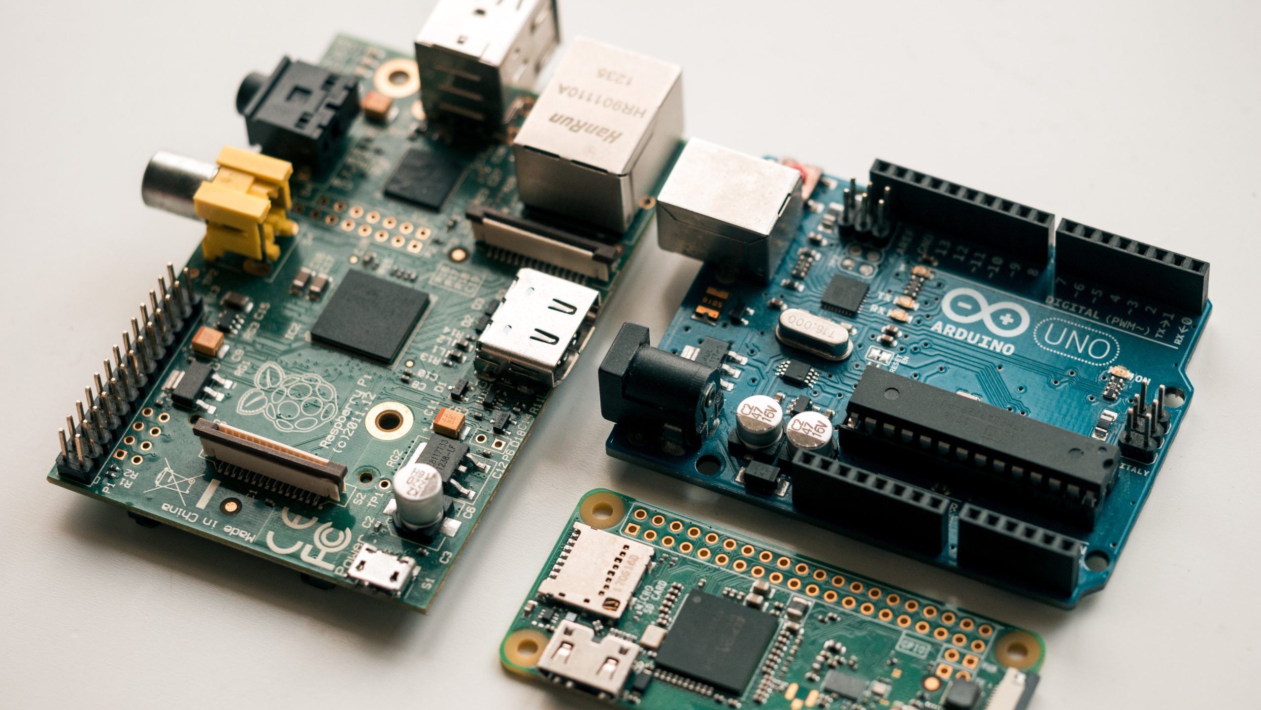
    General purpose computing solutions have been around for decades and have been pivotal in enabling day-to-day computing needs. It ranges from servers, desktops, and laptops to different smart devices.

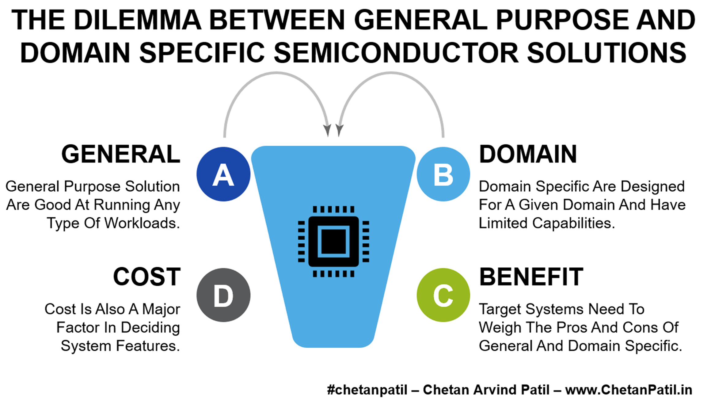
    General: General Purpose Solution Are Good At Running Any Type Of Workloads.

    Domain: Domain Specific Are Designed For A Given Domain And Have Limited Capabilities.

    Similarly, domain-specific computing architecture has provided much-needed bottleneck-free architectural solutions for very high compute-intensive tasks. These applications are only increasing the demand to process more data, for which domain-specific is becoming more critical for such applications than ever.

    Technically, there is a clear distinction between the two (general and domain) types of architectural solutions. However, it is creating a dilemma for existing and emerging companies: Which type of architectural solutions to focus on and invest in as part of a long-term strategy?

    On top of that, it raises the question from the customers on which of the two options to prefer. More so when the new system is mass-produced for years to come.


    Picture By Chetan Arvind Patil

    Deciding to focus on one or the other is not easier. From a semiconductor company’s point of view, it is all about the business margin. It is also the primary reason the emerging semiconductor XPU-focused companies have started to focus on one of the two solutions based on the target market.

    From the customer’s point of view, it all boils down to the benefit and cost impact of opting for one of the two options. It is also where features and long-term support from the chip vendors come into the picture. The target application is another criterion that decides whether a general purpose or domain-specific solution will become handy.

    Benefit: Target Systems Need To Weigh The Pros And Cons Of General And Domain Specific.

    Cost: Cost Is Also A Major Factor In Deciding System Features.

    Apart from all this, the advent of fusion XPU solutions has also started blurring the lines between general purpose and domain-specific solutions. The caveat of fusion solution is the cost and the support of architectural level APIs. These fusion-based products also fall under the heterogeneous domain, which is in the phase of developing the right software platform to enable a smooth transition towards the heterogeneous architectural features.

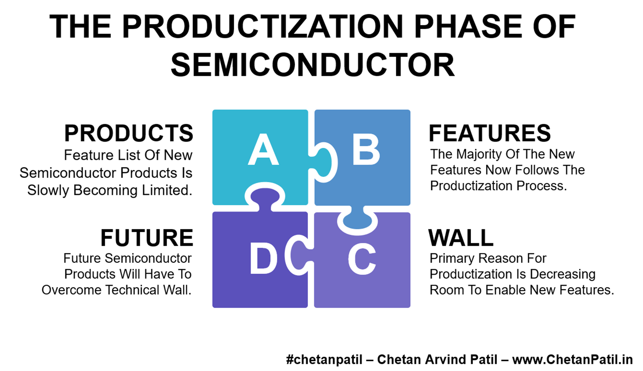
    The need for more powerful and efficient XPUs is only going to increase. General purpose and domain-specific XPU-based solutions provide the required balance of both (performance and efficiency) as per the target domain. However, the feature list of these two different solutions has started to overlap. Sooner or later, it will drive companies and customers to embrace one of the two solutions, or maybe the heterogeneous solution will take over.


  • The Semiconductor And Embedded Systems

    The Semiconductor And Embedded Systems

    Photo by Harrison Broadbent on Unsplash


    Semiconductor companies not only design silicon devices but also (directly and indirectly) power different types of embedded systems. These systems (smart devices, laptops, servers, etc.) cater to consumer and enterprise electronics. And to validate new ideas or prototypes, embedded systems play a crucial role.

    The embedded board has different silicon devices based on the target application. Almost all major silicon solutions (XPUs, Wireless Chipset, etc.) have an embedded solution that allows software and hardware developers to try out new features or even build new types of applications.

    System: Semiconductor Devices Are The Building Blocks Of Different Types Of Embedded Systems.

    Open: Open Embedded Systems Have Enabled Anyone To Explore And Learn About The Different Silicon Blocks.

    Over the last decade, the embedded system domain has become more open source. It now allows anyone to understand the hardware-software interaction and its working and is then used to provide a new type of consumer experience.

    To use embedded systems/boards requires detailed knowledge about underlying silicon architecture. This requirement is also driving the semiconductor knowledge, thus opening up avenues to develop new types of software-hardware systems.


    Picture By Chetan Arvind Patil

    As the complexity of the end system grows, the best way to capture how it will work and not work is via embedded systems. To do so, the companies developing the silicon chipsets often comes up with embedded hardware and software development kit. Which can be used by anyone to try out the next-gen chipset to capture not only features but also how it might or might not fit the future requirements.

    This process has also created open hardware and software embedded ecosystem. It is not only catering to the semiconductor industry but also to the students who want to learn more about the internal workings of memory, kernel, and drivers.

    Ecosystem: Open Hardware Systems Have Led To The Creation Of A New Type Of Software And Hardware Embedded Ecosystem.

    Learning: Embedded System Provides An Easier And Faster Way To Learn More About Different Types Of Semiconductor Silicon Blocks.

    While the embedded system does not directly enable knowledge of how semiconductors work, it does provide a platform for anyone to try out the different types of open hardware to understand internal blocks. On top, the growing software ecosystem also enables new learning and skill building.

    As the semiconductor chipsets become more complex and software-driven, the embedded system knowledge will become very crucial and thus will drive bot the semiconductor and electronic system design industry forward.


  • The Semiconductor Value Of More-Than-Moore

    Photo by Dan Cristian Pădureț on Unsplash


    The semiconductor industry is all about value creation for the business dependent on it. This value is primarily due to Moore’s first law-driven semiconductor product that brought several generations of computing solutions. And, to ensure the value creation process continues forever, More-Than-Moore solutions are now needed.

    The need to bring More-Than-Moore is not due to Moore’s first law not applying to the semiconductor industry. More so, it is still a few decades before the semiconductor industry will run out of ways to pack more transistors while also shrinking the area.

    The fundamental reason to adopt More-Than-Moore solutions is Moore’s second law or Rock’s law, as it is known widely. According to it, the complexity and cost of a new generation of die solutions are doubling every few years and thus leading to a point whereby the ability to pack more transistors will not lead to any favorable cost benefits. The main reason is the capital-intensive semiconductor design, research, and manufacturing processes.

    Law: Moore’s First Law Is Colliding With Moore’s Second Law Or Rock’s Law And Thus Demanding More-Than-Moore Solutions.

    Value: Value Created By More-Than-Moore Era Is Going To Enable New Types Of Products And Solutions.

    The best way to overcome the scenario of Moore’s first law colliding with Moore’s second law or Rock’s law is to bring semiconductor solutions that speed up the growth of More-Than-Moore. It will enable a new generation of silicon products and balances the feature and costs of highly complex semiconductor products, mainly XPUs.

    Overall, the value created by the More-Than-Moore solutions is toward solving the exact problem the semiconductor design and manufacturing industry will face (or already has) in the future. More-Than-Moore provides design-level optimization and can also reduce the cost of manufacturing by leveraging the mix of older and newer technologies.


    Picture By Chetan Arvind Patil

    Today, complex silicon architectures are following the traditional die-level integration and hitting the feature walls, thus demanding new solutions. Something, More-Than-Moore can provide.

    Solutions like chiplets, disaggregated design, and heterogenous packaging are a few More-Than-Moore solutions. These solutions, for now, are costly. However, as the rate of adoption and deployment increases, the cost will slowly go down and eventually will drive new types of silicon solutions that are always bottleneck-free.

    Options: More-Than-Moore Delivers Opportunities To Manage Silicon Level Bottlenecks And Thus Enabling Near-Bottleneck Free Silicon Products.

    Future: Semiconductor Companies That Created More-Than-Moore Solutions Are Seeing The Benefits Of The Future Era.

    Out of all, a critical value created by the More-Than-Moore solutions is: providing options for the computing industry. Chiplets and heterogenous integration have already enabled this path. To further drive futuristic products, the semiconductor industry will have to focus on solutions that can provide customers with better options by embracing the More-Than-Moore-enabled era.

    Semiconductor companies that are working on complex silicon architecture have realized the value the More-Than-Moore era will bring. It is the primary reason such companies are investing in solutions that will become de-facto in the future. The companies that have not started working on such a solution should review the potential the More-Than-Moore era can provide by reshaping the computing world.


  • The Semiconductor Cyclic Impact On Inventory

    Photo by Andrew Gook on Unsplash


    The semiconductor market is highly volatile. Positive or negative demand significantly impacts the end-to-end supply chain. Avoiding scenarios requires equilibrium of supply and demand, which is difficult to achieve due to the several variables of the semiconductor supply system.

    Even with several variables like market demand, manufacturing capacity, cost, and raw material availability, planning is key to ensuring supply and demand are in check. It also leads to an important question of how to achieve a planning-driven equilibrium that ensures the inventory of products good is always as per the market requirement.

    Cycle: Semiconductor Demand Is Dependent On The Cyclic Nature Of The Market.

    Stock: Based On The Demand, The Inventory Of A Given Product Goes Up Or Down.

    Unfortunately, there is no perfect answer for any high-tech industry. The fundamental reason is the time taken to enable supply is rather long and the time to lower the demand is very short. These two opposite processes make it difficult to balance supply and demand.

    While several tools and operational processes are in place to predict the market trend. In reality, the outcomes are not always in line with the real scenarios, and mastering the process of bringing equilibrium of inventory vs demand is not as easy as deploying prediction tools.


    Picture By Chetan Arvind Patil

    The semiconductor industry has always been cyclic, where the demand and supply are not in sync. It often leads to shortages or more than required inventory. Such scenarios are not ideal for the industry and the end customers.

    The standard course of correction that the industry has taken to counter the shortages is by increasing manufacturing capacity. However, the semiconductor manufacturing capacity can never be near-perfect. It is either on the higher or lower side and with new manufacturing capacity, there is also the question of overcapacity, when a downturn in the market severely impacts the semiconductor industry and the major impact is on the inventory created in advance.

    Downturn: In The Case Of A Sudden Downturn, Any Unplanned Inventory Can Cause A Negative Impact.

    Extra: Cyclic Demand And Supply Should Be Considered To Avoid Extra Inventory.

    Such a cyclic nature of semiconductor demand is never going to end. On another side, there seems to be no perfect solution that will justify the cash flow into the manufacturing capacity by ensuring there is always a demand. In reality, there are no control parameters and diverting the existing capacity toward new semiconductor solutions is also not easy.

    Now that the semiconductor industry has started building and opening new semiconductor manufacturing infrastructures, the key question will be how the industry will balance inventory creation by grabbing market demand. If detailed and accurate predictions do not occur, then there is never going to be an end of over or undersupply of capacity, which will in turn impact (positively or negatively) inventory.


  • The Productization Phase Of Semiconductor

    The Productization Phase Of Semiconductor

    Photo by Glen Carrie on Unsplash


    New silicon-powered products should have advanced features. These features also have to differentiate from the existing ones. Otherwise, the probability of success in the market will be very low. On the opposite side, the new semiconductor technology development is slowing down due to the need to find solutions that meet More-Than-Moore requirements. All of this is also delaying new features at the die level. However, the semiconductor industry still has to bring new products.

    Products: Feature List Of New Semiconductor Products Is Slowly Becoming Limited.

    Features: The Majority Of The New Features Now Follows The Productization Process.

    To tackle the dilemma of new features vs the ability to use new technology nodes, a productization path is being taken. Using productization, semiconductor companies can make use of existing and proven technology nodes to drive new features. Even though the design and manufacturing process is not able to use the latest technology node or assembly processes, the end goal of providing new types of products is still achieved.

    What Is Productization: A Process Of Turning An Existing Technology Into An Repeatable Effort To Enable New Products.

    Productization is not always positive news as it hinders the ability to provide more features in the new products. Take the example of XPUs. The rate of launching new XPUs is faster than the ability to enable new semiconductor technology at the die level that makes up the XPUs. On another side, there is a need to keep enabling the computing industry with new types of XPUs.

    To balance these two scenarios, XPU-focused companies take the middle path and keep providing new types of XPUs by leveraging the block level optimization while building new semiconductor technologies that can, later on, provide a needed larger push towards a new era of XPUs.


    Picture By Chetan Arvind Patil

    In many cases, productization can also be taken as a negative scenario. However, it is another business process using which new products get launched to meet the end goal of enabling new products in the market. A similar productization process has been used by different industries including automotive, consumer electronics, and several others.

    When it comes to the semiconductor industry, the fundamental reason to make use of productization is to overcome the technology wall which has hindered the ability to enable next-gen features. While the design processes are still able to make use of old semiconductor technology to enable new efficient products, however, the road to keep doing so is sooner or later going to end.

    Wall: Primary Reason For Productization Is Decreasing Room To Enable New Features.

    Future: Future Semiconductor Products Will Have To Overcome Technical Wall.

    With the rate at which the semiconductor use case is speeding up, productization can help cater to several use cases which do not demand or need the latest semiconductor technology. However, there will come a point where these types of use cases will also need the new silicon-level technology.

    In summary, as part of a long-term strategy, the semiconductor industry will have to cut down the time to enable next-gen semiconductor solutions (mainly nodes, FETs, and lithography solutions). Otherwise, even the productization process will not be able to help in the long term.


  • The Semiconductor Road Towards Chiplets

    The Semiconductor Road Towards Chiplets

    Photo by Luan Gjokaj on Unsplash


    Semiconductor products are struggling to meet the demand to balance power, performance, and area requirements. The challenge to enable efficiency is increasing while there is also a need to meet new technological requirements without adding bottlenecks. Such challenges are slowly becoming impossible tasks whereby the innovation is hitting a technical wall and is now pushing semiconductor design and manufacturing towards a new era.

    To overcome these hurdles semiconductor industry is looking to increase the adoption rate of chiplets. Chiplet is also becoming a stepping stone toward the new era of silicon devices (mainly XPUs) that provide better power-performance management. Such a solution also allows more features while not worrying (for now) about bottlenecks.

    The fundamental reason for adopting semiconductor solutions like chiplets is to ensure that the process technology can be efficiently used by disaggregating the solution across multiple blocks, thus ensuring the critical blocks get the most advanced solutions.

    Market: Semiconductor XPU Market Is Running Into Bottleneck And Chiplets Are The Perfect Way Out Of It.

    Stacking: Scaling Via Stacking Will Soon Run Into Stacking Wall And Chiplets Are Needed To Overcome It.

    However, the adoption of chiplets at a large scale requires a semiconductor road. The inception of the semiconductor road for chiplets is the market, which has been demanding near-bottleneck free features to cater to the world that is processing data.

    Adopting a chiplet solution is to overcome stacking-related thermal and mechanical issues. It has become a concern for XPU-type devices where the need to double the transistors is increasing faster than ever. It has also created new scaling-related hurdles. To solve the scaling bottleneck, chiplets provide a better avenue by allowing the more horizontal area to enable designers and manufacturers to bring new features.


    Picture By Chetan Arvind Patil

    The market requirement is for smaller but powerful silicon devices. It is a must-have for solutions that form the base of on-the-go computing systems like XPUs. However, slowly the ability the integrate more features without impacting the silicon area has become a bottleneck, mainly for the XPU designers. Such a bottleneck directly creates density issues which can potentially lower the performance metric of new solutions.

    Chiplets are by default the better-known solutions to the density-related problem as it allows scaling to be done with the help of packages. However, for chiplets, it is important to consider the cost and time to manufacture. Otherwise, the positive technical impact of chiplets can easily get void by the negative business impact.

    Density: Increasing Silicon Density To Cater PPA Requirement Is Demanding Chiplets Way Of Design And Manufacturing.

    Era: Chiplets Provide The Perfect Avenue To Enter The Era Of Semiconductor Product Development.

    The semiconductor industry is always looking for a solution that can enable a new type of semiconductor product. The ultimate goal of such solutions is to move the computing industry towards a new era. Chiplets do provide an avenue to do so and the semiconductor road taken by the industry has already started enabling a new type of chiplets-driven solutions that are also creating a new level of competition which is eventually going to benefit the industry at large.

    The semiconductor market focused on XPUs is already demanding more chiplets-driven architecture, which in turn is enabling the solution to mitigate near-future scaling and density solutions, and this technical semiconductor road has certainly started the new era for the semiconductor industry and will also enable new types of devices.


  • The Post Act Plan For Semiconductor Manufacturing

    The Post Act Plan For Semiconductor Manufacturing

    Photo by Brett Jordan on Unsplash


    The government of several countries has realized the need to establish a semiconductor ecosystem that can cater to computing needs for decades to come without relying on external factors. In doing so, several new policies and acts are getting approved with the sole purpose that the semiconductor companies will drive the development of an in-country semiconductor ecosystem.

    When it comes to the semiconductor ecosystem, it might never be possible to be 100% resilient and independent. However, it is possible to be 100% resilient and independent in specific parts of the semiconductor product development process.

    Act: Government Driven Acts And Policies For Semiconductor Industry Are Rising.

    Plan: Semiconductor Companies, Mainly Manufacturing, Will Have To Plan Carefully To Make Most Of These Acts And Policies.

    While governments can drive different semiconductor industry-focused acts and policies, the crucial part is the process followed by the semiconductor industry after the government has approved new policies. And, to enable a positive impact demands an error-free plan, and certainly something achievable, from semiconductor companies.

    It should not happen that semiconductor companies are coming up with massive plans of expansion to leverage the incentives, and the execution parts lag. Such scenarios, if occurred, can end up creating a negative impact and might severely push the industry backward.


    Picture By Chetan Arvind Patil

    To leverage new acts, semiconductor companies should focus on the core strength to efficiently utilize benefits. There are several ways to do so:

    Expansion of design and manufacturing.

    Focus on mergers and acquisitions.

    Increase academia-industry collaboration.

    New joint ventures.

    And several other businesses and technology-driven decisions.

    All these approaches are not risk averse. It requires due diligence in the implementation and execution part. Doing so in the semiconductor business is more critical due to the long implementation time and high investment with slower than expected returns.

    Implement: Implementing The Plan By Utilizing The Benefits Provided By The Acts Will Be A Major Task.

    Execute: Execution After Implementation Has To Be Error-Free. Otherwise, The Positive Impact Of Acts Is Not Achievable.

    With new acts getting approved by different governments, there will be a sudden push for expansion. It is where companies will have to be very careful of over/under committing. The goal should be to ensure these acts are to power the next-gen solutions without any delay and cancellation.

    Governments slowly but surely are doing their part by providing the right impetus to enable the expansion of the in-country semiconductor ecosystem. Now it is on the semiconductor industry (mainly core and large companies) to focus on efficient use of the process to ensure continuous development of the semiconductor ecosystem.


  • The Semiconductor Complexity Impact

    The Semiconductor Complexity Impact

    Photo by Andrés Dallimonti on Unsplash


    Building blocks of semiconductor products are shrinking and providing more area to pack new features. It has enabled the industry with options that are eventually powering billions of devices around the globe.

    Such proliferation is positive news for the semiconductor industry and industries that benefit from such development in semiconductor technologies. On another side, bringing this positive change requires creating complex semiconductor devices. Over the years, the complexity of such devices has increased and has started impacting different stages of the semiconductor end-to-end product development stages.

    Design: Semiconductor Design Is Becoming Highly Complex Due To The Need To Pack More Features Without Compromising On The Silicon Area.

    Manufacturing: Complex Semiconductor Designs Create Manufacturing Challenges And Hurdles Which Leads To Longer Manufacturing Cycle Times.

    Design by itself has become more challenging due to the need to incorporate a new types of devices. Profiling of these devices (FET) is needed to ensure the data correlates with the expected outcomes. After this, the design can use such a new device in large numbers. However, still, system-level accurate characterization is needed. All of this is time-consuming and also impacts the overall development cost.

    On the manufacturing side, proving new semiconductor technologies without any significant yield or process issues is another challenge that a complex process brings. One such challenge is the possibility of a higher rate of defectivity, and mitigating or capturing defects requires adding extra steps that can stretch the cost and time.


    Picture By Chetan Arvind Patil

    Complex architectures like XPU are the first to incorporate the most advanced solution possible. During the initial evaluation phase, these advanced XPUs can show possible defects due to a new device-level solution. In many cases, it is also a primary reason why semiconductor companies developing XPUs with new semiconductor technology spend years in research and development activity before releasing the product for mass-market.

    There are several ways to ensure the new device level (power, thermal, or performance) features do not lead to any defects. However, it comes up with a significant increase in a process step and can lead to higher development costs during the design and the manufacturing validation phase.

    Defect: Packing More Features Leads To Complex Semiconductor Flow That Can Introduce Defects And Derail The Production Plan.

    Cost: Complexity Of Semiconductor Products Also Comes At A Higher Cost Of Design And Manufacturing, Thus Questioning Affordability.

    Apart from the development stages getting complex and costlier, the process to ensure the new products are a market fit also keeps increasing due to new devices that are beneficial only if the end-system benefits from such device-level designs. As the complexity of devices enabling new features gets more complex, the semiconductor industry will have to find ways to lower the overall impact on the cost, defectivity rate, and the design to manufacturing cycle time.

    The future of semiconductor devices is going to be more complex than ever. Thus, enabling an efficient development process that reduces the overall negative impact on the end-to-end development cycle is key to ensuring more time for a cost-sensitive process. Otherwise, the overall long-term impact might not benefit the semiconductor industry.


  • The Already Advanced Semiconductor Manufacturing

    The Already Advanced Semiconductor Manufacturing

    Photo by Robert V. Ruggiero on Unsplash


    Advanced manufacturing is one of the most important development and is pushing manufacturing (across industries) towards a new era. Several criteria decide whether a given manufacturing industry stands to call itself an advanced one. These criteria (not set) have been around for a while, and the manufacturing world is embracing the changes to enable advanced features to provide quality products to the market.

    What Is Advanced: Solutions Deployed In Manufacturing Environment That Improves Productivity, Quality, And Time-To-Market But Still Requires Human Guidance.

    There are four information points to identify the advanced manufacturing industry. These are Data, Equipment, Process, And Automation. Together, these four attributes provide a clear view of advanced manufacturing.

    When it comes to the semiconductor industry, these four feature points are already in use for a long time. Thus, it will not be wrong to say that the semiconductor industry is already in the advanced mode and might be marching towards the super-advanced phase.

    Data: Capturing And Analyzing Semiconductor Manufacturing Data Is Already A Well-Established Process.

    Equipment: Semiconductor Manufacturing Flow Is Already Equipped With Advanced Equipment.

    Data, for example, has been a part of semiconductor manufacturing for decades. It has enabled flavors of processes and also captures issues on the go, a must-have feature for advanced manufacturing. Similarly, the high-level and never-used equipment that creates billions of devices in the smallest area is already part of the semiconductor industry, another must-have advanced manufacturing process.


    Picture By Chetan Arvind Patil

    On top of the data and equipment, the semiconductor industry also has several process checks to make the products without any errors. This process has been key to enabling silicon products to reach billions of people around the globe. The fundamental reason these processes have become error-free is due to the automation usage in semiconductor manufacturing.

    Process: Semiconductor Design And Manufacturing Process Are Already Designed To Be Error-Free.

    Automation: Automation In Semiconductor End-To-End Flow Is Already At An Advanced Stage.

    With all these advanced manufacturing features already deployed as part of process control, the question is – what is the next step? The next logical step might be the step toward super-advanced manufacturing.

    What Is Super-Advanced: Solutions Deployed In Manufacturing Environment That Improves Productivity, Quality And Time-To-Market Without Human Input.

    Super-advanced manufacturing will remove the need to provide human input at any process step. While the semiconductor manufacturing process is already capable of working without human effort, there are still several areas where process error correction requires human intervention. In super-advanced manufacturing, human intervention will be none. However, semiconductor manufacturing will take several years (even decades) to achieve this state.

    As new FABs and OSATs come around the globe, the deployment of advanced manufacturing will increase further and might also pave the way for the super-advanced semiconductor manufacturing roadmap.


  • The Growing Need To Adopt Multi-Technology Semiconductor Fabrication

    The Growing Need To Adopt Multi-Technology Semiconductor Fabrication

    Photo by Henry & Co. on Unsplash


    The semiconductor fabrication process is complex and costly, and it takes a lot of time to fabricate advanced solutions. Apart from the technical and business hurdles, the ability to develop one specific type of semiconductor device node is not resource-friendly. It also drives the demand to continuously invest in new facilities, which may or may not be ROI friendly.

    Multi-Technology Semiconductor Fabrication: Either Two Existing In-Demand Technology Can Be Fabricated At The Same Facility Or At Least Allow The Ability To Quickly Re-Spin The Existing Facility To A New One.

    This problem is getting more expensive with the launch of advanced technology nodes that require a new type of process flow, material, and equipment, which in turn requires a dedicated new facility. It is also evident from the number of fabrication facilities that are coming up and are focused on technology that will drive the semiconductor industry towards the angstrom phase.

    Long: With Every New Semiconductor Process Technology, The Fabrication Process Is Becoming Longer.

    Multi: Fabrication Facility Should Provide Multi-Technology Node Option Or Have The Ability To Expand Easily.

    The big question is whether there is a process to minimize the impact of the new advanced node on the need for dedicated and new facilities? The short answer might be no, but strategically it should be possible to develop a new facility with a focus on the ability to enable multi-technology processes today or tomorrow.

    It certainly does not mean that the overall cost will be lower when the time comes to enable optional technology. However, if planned well, solutions to parallelize the fabrication of multi-technology in the same facility today or at least how to minimize the future upgrades (apart from spinning off a new facility) to lower the overall expenditure should be feasible.


    Picture By Chetan Arvind Patil

    In many cases, the ability to focus on current and future technology nodes are not feasible due to the different support system required to enable future technology. At the same time, the fabrication cost of existing technology is increasing. This cost will go up further for the next-gen technology. Thus, re-planning and re-investing (following Moore’s law) becomes a lengthy process that is not always technology and business-friendly.

    Incorporating multi-technology where either two existing in-demand technology can be fabricated at the same facility or at least allow the ability to quickly re-spin the existing facility to a new one is the need of the hour. Today, there are clusters of fabrication facilities nearby that cater to different technology nodes. However, each of these demands dedicated resources that double the amount of investment.

    Cost: Moving From Single To Multi Will Allow Greater Control Over Fabrication Cost.

    Time: Time To Bring New Technology In A Multi-Technology Fabrication Can Become Shorter.

    The number of semiconductor manufacturing companies focusing on advanced nodes is limited. If the cost to bring in future technology grows further, it will reduce the number of semiconductor manufacturers focused on advanced nodes. Overall, it will make the semiconductor supply chain very fragile, and solutions to mitigate such situations are needed.

    Multi-technology can be a way to adopt multiple technologies today and build a facility for both together. It can also be an avenue to make future technology nodes more resource friendly. It will also demand additional work and capital. However, preparing for two technology or running two in parallel (in collaboration with equipment, material, and other technology providers) can certainly open up an option to lower the future semiconductor manufacturing cost.