Author: admin

  • The Need To Integrate Semiconductor Die And Package Roadmap

    The Need To Integrate Semiconductor Die And Package Roadmap

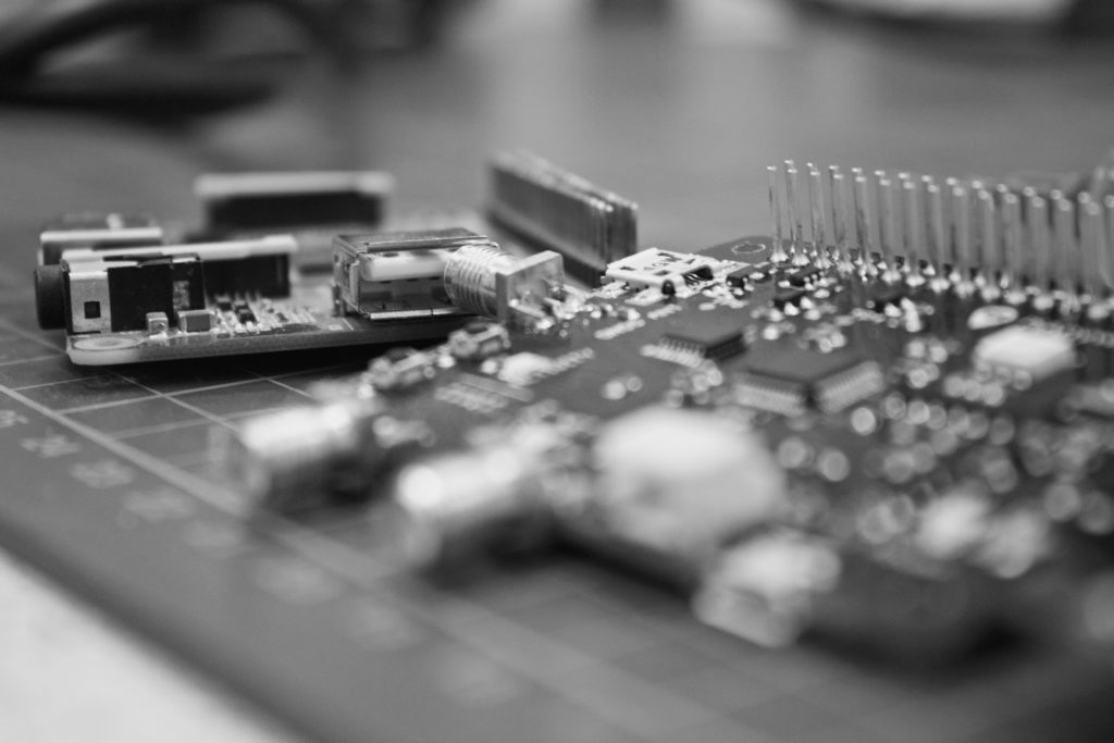
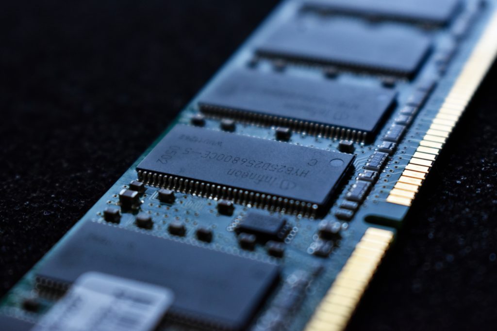
    Photo by Vishnu Mohanan on Unsplash


    Several semiconductor industry-wide roadmaps are planned and released by semiconductor companies and also different technical semiconductor groups. These semiconductor roadmaps are vital in providing glimpses of future semiconductor technologies and how they will shape silicon products.

    Out of all the semiconductor roadmaps, the two most critical are the die roadmap and the package roadmap. These two roadmaps are drafted by separate technological groups apart from different roadmaps from semiconductor companies. There is no question that these roadmaps provide a way to design and manufacture next-gen silicon products to transform industries relying on semiconductors.

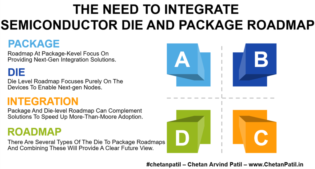
    Package: Roadmap at package-level focus on providing next-gen integration solutions.

    Die: Die level roadmap focuses purely on the devices to enable next-gen nodes.

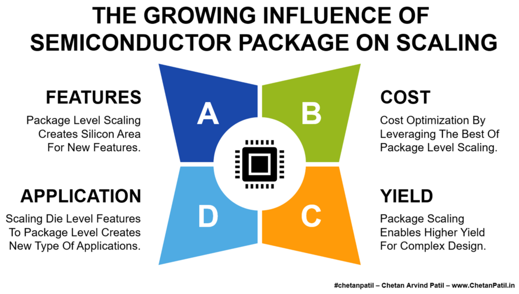
    However, today, the semiconductor industry is at the cross-section where the die and package solutions complement each other. In doing so, these two semiconductor technologies are pushing the semiconductor industry to adopt More-Than-Moore solutions. This intersection of technology and business goals should be the primary reason the semiconductor industry should find an integrated roadmap to provide a clear view of die and package solutions that can come together to provide more advanced solutions than ever.

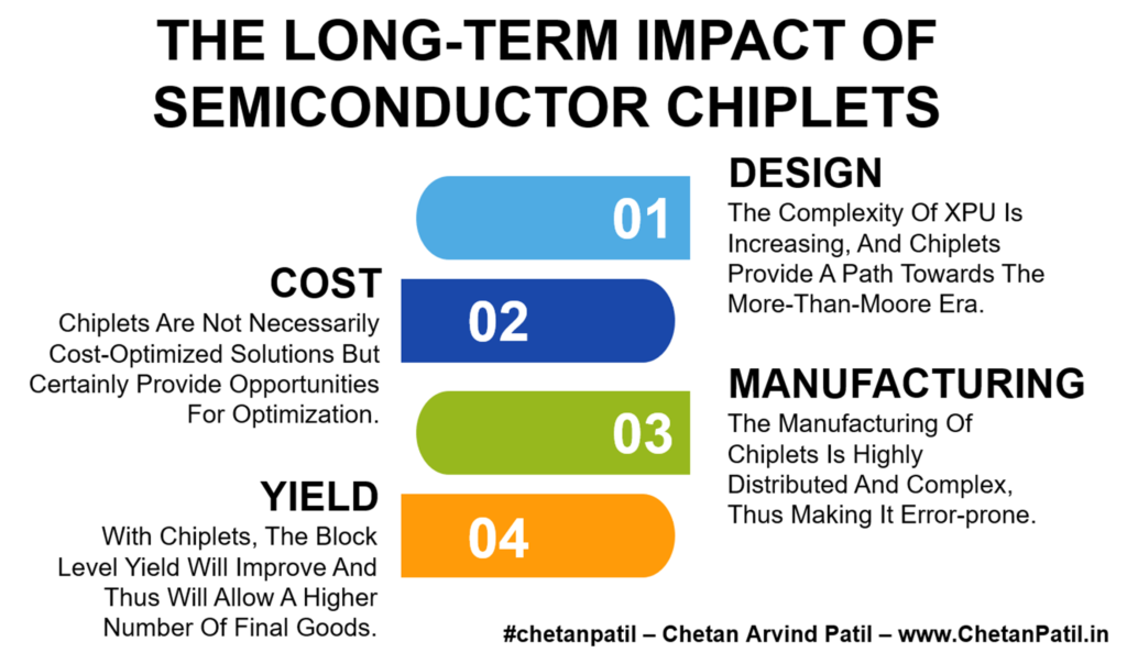
    Combining die and package-level roadmaps will also allow faster development of support systems. One example is chiplets, which need universal standards to combine die and package-level components to provide robust, economical, and industry-friendly More-Than-Moore solutions.


    Picture By Chetan Arvind Patil

    There is no denying that individual die and package-level roadmaps have sections that focus on solutions to provide a common technological platform. Even then, when it comes to implementation, several bottlenecks are present in the design to manufacturing stages. These bottlenecks range from technical (standards, yield, material, etc.) to business issues (cost, capacity, etc.). An integrated roadmap with a focus on how the industry can overcome these challenges is needed.

    An integrated roadmap can also provide a clear view to enable flawless integration of next-gen die and packages to drive faster adoption towards the More-Than-Moore era.

    Integration: Package and die-level roadmap can complement solutions to speed up More-Than-Moore adoption.

    Roadmap: There are several types of the die to package roadmaps and combining these will provide a clear future view.

    Advancement in die and package-level solutions will continue for decades. Also, the need to stack dies and packages to provide integrated solutions for the architectures like chiplets and flexible electronics will continue to rise.

    Thus, for the angstrom era and the long-term innovation in the semiconductor industry, faster adoption of integrated design and manufacturing approaches for the die and package scaling will be crucial. Achieving this goal will require continuous work on an integrated die and package roadmap.


  • The Long-Term Impact Of Semiconductor Chiplets

    The Long-Term Impact Of Semiconductor Chiplets

    Photo by Louis Reed on Unsplash


    Chiplets are changing the way complex products like XPUs getting designed and manufactured. Its impact is how modular the new XPU solutions are becoming. This modularity is paving the way for new-age IP-driven XPU design and manufacturing and opening up features that were not easy to deploy due to the need for the aggregated approach.

    As with any new semiconductor process and technology, the vital factor is the long-term impact of such new solutions. In the case of chiplets, it has already started to impact design and manufacturing methods.

    The positive long-term impact of chiplets is providing the ability for XPU developers to enable solutions in the angstrom era by leveraging the disaggregated approach. It is also opening up a new design approach that allows chip architects to leverage different types of IP blocks and also provides the ability to enhance block-level processing capability due to the disaggregated manufacturing.

    Design: The complexity of XPU is increasing, and chiplets provide a path towards the More-Than-Moore era.

    Cost: Chiplets are not necessarily cost-optimized solutions but certainly provide opportunities for optimization.

    From the cost point of view, chiplets may be costly to manufacture due to the die level disaggregation that will require multiple silicon wafers and capacity. The manufacturing flow will also become more complex. Until the chiplet adoption speeds up, the early adopters will have to spend more capital.

    However, as the adoption increases, the manufacturing processes are bound to become optimized. It will then drive better cost-optimized manufacturing of chiplets-driven XPUs.


    Picture By Chetan Arvind Patil

    Distributed processing of chiplets at the manufacturing side brings new challenges. More so when the packaging of chiplets becomes a critical process. The complex manufacturing flow on the packaging side can drive a higher error rate if the process is not validated correctly before mass production.

    There are processes available to ensure the new manufacturing process (chiplets) leads to positive results. However, until the chiplets-inspired chips are mass-produced, there will always be a possibility of errors and such errors will impact yield and cost.

    Manufacturing: The manufacturing of chiplets is highly distributed and complex, thus making it error-prone.

    Yield: With chiplets, the block level yield will improve and thus will allow a higher number of final goods.

    The aggregated approach of XPU design and manufacturing does not often lead to higher yields. Disaggregated manufacturing of chiplets enables higher yield. Mainly due to the ability to take the complex critical blocks as separated die.

    Chiplets design and manufacturing methods are still in the early days. As adoption and usage grow, the positive and negative long-term impacts will be more visible. Meanwhile, today, chiplets are indeed the most promising More-Than-Moore era solutions.


  • The Ever Increasing Cost Of Semiconductor Design And Manufacturing

    The Ever Increasing Cost Of Semiconductor Design And Manufacturing

    Photo by Anne Nygård on Unsplash


    The complexity of semiconductor devices is increasing at a rapid pace. The reason is the demand for new features, which requires novel design and manufacturing approaches, which come at a higher cost due to the time, resources, and investment needed to enable new semiconductor solutions.

    On the design side, it has become easier to bring up new solutions and prove them using an advanced simulation approach. Eventually, these solutions should be fabricated and validated, which costs millions of dollars, and with every next-gen design and manufacturing process, the cost of prove-in keeps increasing.

    Design: Complex solutions demand time and resources, which increases the cost of new solutions.

    Manufacturing: Bringing new solutions to the market means investing in new-age manufacturing facilities.

    The connected (equipment, material, raw wafers, tools, and so on) semiconductor supply chain can also delay the plans, which increases the cost of introducing new solutions.

    Semiconductor companies have to manage and plan future market requirements so that the new solutions are not too costly to develop. On another side, given that the semiconductor industry is highly connected and driven by the connected semiconductor supply chain, it is not easy to keep the cost of development low.


    Picture By Chetan Arvind Patil

    The design and manufacturing of semiconductor products are dependent on several technical factors. Apart from it, there is a business aspect (market-driven) that also impacts the total cost of semiconductor product development.

    Higher demand for semiconductor products increases the need to produce more silicon chips. However, not being able to fulfill these requests on time eventually adds to the negative cost. On another side, the supply constraint of any goods needed by the semiconductor process (manufacturing equipment, wafers, materials, etc.) can increase, thus directly impacting the overall design and manufacturing cost.

    Demand: Continuous investment to meet market demand adds to the overall cost of semiconductor product development.

    Supply: Increase in the cost of a connected supply chain directly impacts the semiconductor design and development.

    This cyclic nature of demand and supply also impacts the total cost of the semiconductor industry, more so when there is a need to add new capacity to bring supply-demand equilibrium.

    As the semiconductor industry embarks on a new era of design and manufacturing processes, the need to balance the cost to enable affordable market solutions will be crucial. Otherwise, it will not be easy to drive the faster break-even point for the next-gen capacity, which will also shape the future of several semiconductor manufacturing companies.


  • The Growing Influence Of Semiconductor Package On Scaling

    The Growing Influence Of Semiconductor Package On Scaling

    Photo by Christopher Bill on Unsplash


    Advancements in package technology are as vital as advancements in technology nodes. These two semiconductor solutions enable silicon products to work per the required specifications. Technology node innovation has occurred more rapidly than package technology. Given that now the technology node is going to hit the node wall, it is time for package technology to provide avenues to shape the future of next-gen silicon design and manufacturing.

    The semiconductor package has always been an integral part of semiconductor manufacturing. It has shaped and powered different silicon features and cost-optimized solutions for several decades. Semiconductor package technologies also ensure that the end-product can withstand harsh operating conditions by managing different thermal, chemical, physical and mechanical characteristics.

    Features: Package level scaling creates silicon area for new features.

    Cost: Cost optimization by leveraging the best of package level scaling.

    The focus on package technologies has further grown in recent years. The primary reason is the diminishing die-level scaling opportunities, which raises questions on how the next era of silicon devices will evolve in size, shape, feature, efficiency, and performance. The answer lies in the semiconductor package evolution.

    For the last decade, semiconductor package technology has consistently shown the ability to spread the die-level blocks across the different layers with the help of connections via industry-standard interfaces. It provides avenues to continue scaling for high-performance die blocks and thus deliver higher than ever capabilities.

    The impact of such solutions from the semiconductor packaging world is evident in heterogeneous architectures like chiplets, and the influence of such packaging qualities will grow in the coming years.


    Picture By Chetan Arvind Patil

    Scaling beyond a certain point, at the die level, is complex and error-prone. It is also getting costlier and time-consuming to keep enabling die-level optimization to package more devices for better features and performance and thus pushes the industry toward package-driven scaling features.

    The advanced package technology to enable scaling allows better yield. On top, the risk of introducing errors is far less than other scaling options.

    Yield: Package scaling enables higher yield for complex design.

    Application: Scaling die level features to package level creates new type of applications.

    Apart from the yield, taking advantage of new types of packaging solutions also provides routes to design and develop new applications. It is evident from the powerful and portable solutions package technology-driven chiplet has started to enable. Similarly, different types of flip-chip solutions will soon power next-gen applications that will be far more efficient than what is available in the market today.

    The influence and impact of package technology are only going to grow further, and it has already become a crucial pillar in enabling next-gen devices. Semiconductor companies which incorporate the best of both die and package level scaling will eventually be able to launch better products.


  • The Importance Of Capturing Semiconductor Data

    The Importance Of Capturing Semiconductor Data

    Photo by Anne Nygård on Unsplash


    Data has become a vital commodity in today’s market. The same is valid for the semiconductor industry. More so when the cost to capture the semiconductor data is rising. The semiconductor data capturing is directly tied to the process level solution that demands high-cost LAB and FAB to enable data collection to make accurate decisions.

    Rock’s Law (Moore’s Second Law) states that the cost of building a semiconductor manufacturing facility doubles every four years. However, in the last few years (market dynamics), Rock’s Law is not only changing in terms of cost but also time.

    Today, the cost doubles every two years (or even less). It is primarily due to the faster advancement in the technological solution that is creating the need for next-gen equipment and processing tools. All of this implies that the total cost of manufacturing is increasing.

    Escapes: Capturing relevant semiconductor data prevents design to manufacturing escapes.

    Cost: Mitigating cost by capturing issues before they occur demands accurate use of semiconductor data.

    As the cost of manufacturing increases, so does the cost of generating the data out of silicon. Without semiconductor data, escapes get introduced during the manufacturing phase, and if an escape does occur, it can add unnecessary costs.

    Semiconductor data accuracy becomes more relevant when the silicon can be active in the field for a very long time (years to decades). Any failure can then have a catastrophic impact on the customer and eventually impacts overall product quality.

    While the cost to generate the silicon data to enable next-gen devices is increasing. On another side, it is also vital to keep investing in tools to drive data-driven semiconductor product development.


    Picture By Chetan Arvind Patil

    Semiconductor data also plays a crucial role in enabling planning while driving quality products. Planning aspects come into the picture when the process of die-level data is collected to dive into futuristic device development. Without the semiconductor data, the designers and manufacturers cannot plan the roadmap for next-gen devices to improve the performance and the quality of the products.

    Data via simulation is helpful up to a certain extent. For long-term manufacturing investments, short-term investment is required to enable the validation of silicon products. And doing so requires investing in LABs to capture relevant silicon data, which is a time and cost-demanding process.

    Quality: Semiconductor data empowers designers and manufacturers to provide high-quality products.

    Planning: Semiconductor data is also important to enable next-gen design and manufacturing processes.

    The semiconductor industry is planning for the world beyond 2nm, and implementing such plans demands silicon data that can prove the solutions work out in reality. On paper (via simulations), the planning can only go out to a certain extent, beyond which companies need to drive validation via CapEx.

    The semiconductor data is getting costlier. However, semiconductor companies still have to keep investing to capture relevant data to mitigate escapes. On top, data enables quality products and robust (technical and business) planning. If semiconductor companies are planning for manufacturing capacity, then they should always account for the semiconductor data cost and its positive impact.


  • The Semiconductor Race To Scale Technology

    The Semiconductor Race To Scale Technology

    Photo by Jeremy Thomas on Unsplash


    The technology roadmap for the semiconductor device level scaling is updated yearly. However, implementation demands several years of continuous effort. It is also why only a few semiconductor manufacturing firms can follow the technology scaling roadmap accurately.

    For semiconductor design and manufacturing companies to stay ahead of the scaling curve demands years of planning. It ranges from a specific node to scale, the solution to focus on, new types of devices and working with the equipment industry to support next-gen solutions. On top of all this, whether there is a market that demands building new technology node capacity.

    Resources: Scaling technology demands many capital-intensive design and manufacturing resources.

    Execution: Utilizing resources to drive perfect execution is key to enabling next-gen scaling solutions.

    Planning such a large set of technology to business points demands time and resources, something not all semiconductor design and manufacturing companies can afford to do. It also limits the number of semiconductor companies that work toward advanced nodes.

    Gathering the required resources and executing them without any issues is also a big task for manufacturers who can afford to do so. There are already several examples of this based on 5nm, 3nm, and 2nm, for which several experienced companies struggle to come up with scaling solutions on time.


    Picture By Chetan Arvind Patil

    Scaling technology is for sure about how resources execute the strategy. Eventually, execution also relies on how the market and product fit is and might be the driver of why not all companies focus on products that demand advanced next-gen scaling solutions and thus have a different market than the rest.

    Based on the historical technology roadmap, the market for new scaled solutions will always exist. However, the question remains on how to fit the product into the market. Thus without a clear path toward the type of products that will eventually find use in the advanced nodes, it is not easy to adopt a strategy to scale semiconductor technology.

    Market: Focusing on the need to find the fit for the new scaling solutions is also a crucial part of the process.

    Product: Companies have to focus on new products that correctly uses scaled semiconductor technology.

    Market-product fit becomes more vital for costly, complex, and advanced nodes. The primary reason is the area of application, which is very limited. It implies that the focus needs to be on niche products, which brings a new set of challenges for even the most experienced and resourceful companies.

    The race for scaling next-gen technology is not going to end soon. The number of players participating will decrease, and those who can balance the resource and execution strategy along with a perfect product-market fit will eventually find success.


  • The Semiconductor Learning From The Capacity Crisis

    The Semiconductor Learning From The Capacity Crisis

    Photo by Liam Briese on Unsplash


    In the last two years, the semiconductor manufacturing capacity has seen all the ups and downs it could have. From rising silicon demand to overflowing orders to capacity crunch to building new futurist capacity, all of these in a short period. In the end, the semiconductor manufacturing enterprises could fulfill orders based but not without long cycle times.

    The overflowing orders without the ability to cater to all requests in the standard cycle time have been a steep learning curve for semiconductor companies and semiconductor-dependent industries. This learning ranges from finding the weakest link to empowering better forecasts via data and planning.

    Weakest: Finding the weakest link in the semiconductor chain and making it the strongest one is vital for future growth.

    Forecast: Robust forecasting by considering semiconductor industry and non-semiconductor industry data points.

    Focusing on the weakest link and planning is the key to leveraging time to prepare for future demands. Today, the weak link in semiconductor manufacturing is capacity. The semiconductor industry has started the journey to turn the weak link into the strongest one. However, the time taken to do so will be years (maybe decades), and till then the capacity constraints will exist.

    Forecasting is another learning that the semiconductor capacity crunch has brought. No one saw the sudden spike in demand leading to the overflowing capacity request. Also, the forecasting (a big part of any manufacturing industry) for such scenarios was not realistic and should have considered several factors apart from what is relevant and not relevant to the semiconductor industry.


    Picture By Chetan Arvind Patil

    Finding the weakest link and enabling accurate forecasting requires data-driven planning. Semiconductor manufacturing capacity needs to consider different types of data points that come from the core semiconductor business but the happenings around the world and how they may or may not impact the semiconductor industry.

    Considering different industry data points also empowers the semiconductor industry to plan based on where the market is heading and how situations like the pandemic positively or negatively impact it. It will surely enable more robust planning than ever.

    Data: Capturing data points from sources (semiconductor and non-semiconductor) to enable efficient forecasting and planning.

    Planning: Understanding forecasting data points to drive next-gen planning and project-to-product expansions.

    Semiconductor manufacturing capacity planning is capital-intensive and time-demanding. It directly implies a robust strategy is needed to cater to different types of market demand. A data-driven approach helps create error-proof planning. Doing so also enables semiconductor manufacturers to balance next-gen solutions alongside customer needs driven by market requirements.

    There are numerous lessons learned due to the semiconductor manufacturing capacity crisis. Out of all, finding the weakest link to enable robust forecasts by utilizing data to plan future execution are the four major course corrections the semiconductor industry needs to focus on to drive shortage-free future growth.


  • The Impact Of Lithography On Semiconductor FAB

    The Impact Of Lithography On Semiconductor FAB

    Photo by Laura Ockel on Unsplash


    More than 50% of the semiconductor FAB (fabrication) cost is due to equipment and tools. Any given FAB has hundred different types of these, and without the required tools and equipment, the FAB cannot work efficiently. One piece of equipment that drives the semiconductor fabrication process forward is lithography.

    There are several aspects of semiconductor fabrication that has driven by lithography equipment. Yield and defect are two such examples from the technical point of view. It is the primary reason why semiconductor fabrication focuses a lot on which type of lithography technology to deploy. Eventually, products with low yields and high defect rates will not be market-qualified.

    Yield: Lithography equipment plays a vital part in achieving the required target process yield.

    Defect: Defect free masking is an important part of semiconductor fabrication made possible by lithography.

    Yield and defect are also dependent on the complexity of the semiconductor product. However, lithography equipment is supposed to handle the complex process. With semiconductor manufacturers focusing on next-gen advanced technology nodes, the importance of error-free lithography equipment will increase further.

    Semiconductor process technology is dependent on lithography and plays a crucial part in deciding how the FAB throughput will be. It is why semiconductor manufacturers worldwide are focused on acquiring the latest lithography equipment to upgrade existing FABs or build a new ones.


    Picture By Chetan Arvind Patil

    From a technical point of view, lithography equipment plays a vital role, and apart from yield and defect, there are more process-related criteria that lithography fulfills. However, from the business side too, the lithography equipment plays an important part.

    Two ways in which lithography equipment helps from a business point of view are capacity and break-even point. When it comes to building or upgrading FABs, lithography decisions are crucial. The reason being the solutions that the semiconductor FAB wants to make should be proven with different process steps, including the one executed by the lithography. In many cases, lithography often becomes the bottleneck due to the complex process.

    Capacity: FAB expansion and upgrade are directly related to the lithography equipment performance.

    Break-Even: Lithography also plays a critical role in achieving the FAB Break-Even Point.

    Semiconductor FAB capacity is directly associated with lithography due to the process node. The majority of the semiconductor FABs are opting for a new process node, and the decision on which type of xUV technology to use becomes an important parameter. Lithography also allows FABs to achieve faster break-even by continuously processing large numbers of defect-free and good-yielding wafers.

    Semiconductor capacity building is speeding up, and with technical/business impacts, lithography will play a big part. There are several concerns about lithography equipment shortage, and the path to successfully operating the new FAB will not be easy. Semiconductor manufacturers will have to focus on mitigating the lithography equipment shortage so that the investment done has a long-lasting impact.


  • The Semiconductor Race Between SPU and TPU

    The Semiconductor Race Between SPU and TPU

    Photo by Lukas on Unsplash


    Processors are an integral part of any computing device. For the last few years, the importance of providing efficient and high-performance processors has only grown over the decade. It has thus shifted the design and manufacturing aspect of processing units, thus enabling the transition towards specialized processing units apart from focusing on traditional processor units.

    Traditional Processing Units (TPU) have been around for decades and have successfully catered to the general-purpose processing market like laptops, desktops, edge devices, and servers. TPU thus has made a long-lasting impact that has shaped different types of solutions and will continue to do so for years to come.

    SPU – Specialized Processing Units – Designed and manufactured to handle specific data processing task.

    TPU – Traditional Processing Units – Designed and manufactured for the general-purpose computing world.

    On another side, to enable a new computing market, Specialized Processing Units (SPU) are being launched. SPUs fundamentally differ from TPUs concerning the underlying data and memory architecture.

    However, the market demand is now pushing the need to create more specialized and custom XPUs, leading to the rise in demand for SPUs. It does not mean TPU will lose out on the market but certainly will have to raise the technical features to meet up with the solutions that SPU can provide due to the ability to create new types of computer architectures.


    Picture By Chetan Arvind Patil

    TPU and SPU are differentiated based on the features they provide. TPUs are focused on enabling traditional processing that helps in day-to-day computer applications. On the other side, SPU has specific cores and silicon devices to enable more special processing like neural computing or data modeling.

    TPU can have SPU features, but the cost due to the increase in complexity does not justify the business potential for the mass market. It has prompted semiconductor processor-focused companies to launch SPUs as separate products apart from TPUs.

    Feature: Features provided are a major differentiating factor between SPU and TPU and raise the complexity of these devices.

    Cost: SPU And TPU are designed for different markets, but slowly the gap is reducing, and both these solutions will cater to the same market.

    Design and manufacturing associated with SPU and TPU are other differentiating factors. SPU mainly demands new semiconductor technologies that often raise the cost and time to market. As the focus on adaptive XPUs grows, the feature list of TPU and SPU will increase.

    The race between TPU and SPU has already started and is pushing semiconductor companies to launch both TPU and SPU products. Given the focus on computing processing demand, the race between TPU and SPU will not end soon.


  • The Bottlenecks For Semiconductor Silicon Brain

    The Bottlenecks For Semiconductor Silicon Brain

    Photo by Daniel Pantu on Unsplash


    The race to create computer architecture that mimics the human brain has led to the creation of neuromorphic architectures, and there is not a single computer architecture-focused semiconductor company that has not launched neuro-inspired silicon chips.

    However, creating a very large-scale neuromorphic XPU is not only complex but also costly. The applications are limited and do not justify the business case. On top, there are technical and business bottlenecks that do not favor mass-market neuro-inspired chips.

    Design: Brain-inspired silicon design is complex, and design methodologies are not suitable for neuro-inspired XPUs for the mass market.

    Manufacturing: Yield and cost are big bottlenecks that are stopping the mass production of neuro-inspired XPUs.

    The fundamental bottlenecks for a mass-market neuro XPU is design complexity coupled with manufacturing hurdles. On the design side, the major hurdle is how to pack more neuro (limited to a few million) without impacting performance. From the manufacturing side, the neuro-inspired chips are using the advanced node, and getting a higher yield with such complex architecture is not an easy task.

    Bringing neural-inspired chips to the mass market will require balancing the design with manufacturing so that the design features reflect on the manufacturing process without worrying about the yield and thus the overall cost.


    Picture By Chetan Arvind Patil

    Design and manufacturing hurdles are the first two bottlenecks in bringing brain-inspired silicon to general processing. On top of these two, the market requirements and the specific application demands are also the reason why brain-inspired computing is still limited to specific domains.

    In general, the big market for the processing world demands low-cost solutions and any silicon with neural processing (beyond NPU blocks) raises the cost of design and manufacturing. The applications of neuro-driven silicon chips are also specific and day-to-day consumer solutions do not demand such a high specific level of processing which is another bottleneck in bringing neuro chips to the mass market.

    Market: The market for neuro-driven XPUs is niche and yet to evolve to drive faster adoption of XPUs.

    Application: Applications of neuro-inspired XPUs are specific to the server side and bringing them to the consumer side will demand unique applications.

    Even after such bottlenecks, the XPU-focused semiconductor companies are designing processing blocks that are neuro-inspired, and slowly the percentage of silicon area that is becoming neuro-inspired is growing year on year.

    For the next decade, neuro-inspired XPU will be specific to large data processing. However, as the design and manufacturing march toward advanced semiconductor technologies, the percentage of the neuro-inspired silicon blocks will soon grow from 10% to 100%.