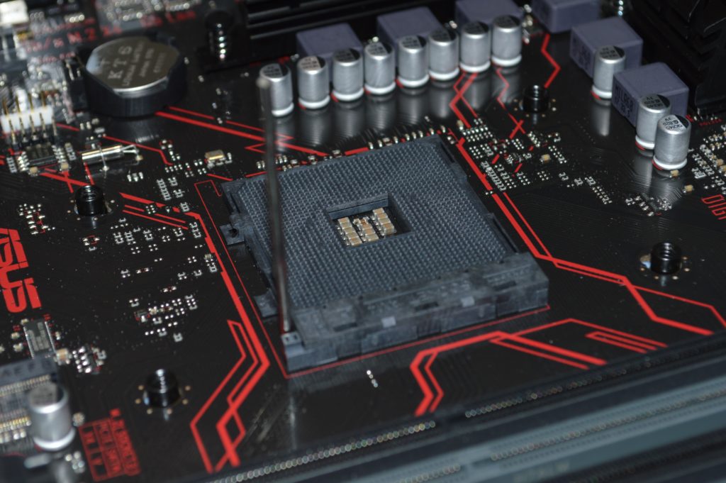
Photo by Testalize.me on Unsplash
Semiconductor manufacturing cost is increasing year on year. The reasons are the high cost to develop new semiconductor manufacturing processes, which often requires constant up-gradation of facilities.
As semiconductor manufacturers expand to new regions, the most critical piece will be the push for innovation. The semiconductor technologies used in the semiconductor product development process have to be defect-free, which demands innovative solutions. It is the primary reason semiconductor companies keep coming up with new technology node processes apart from package technologies.
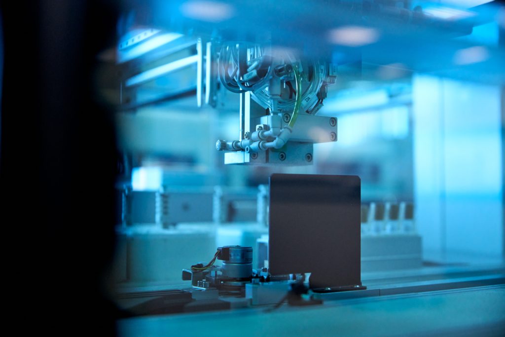
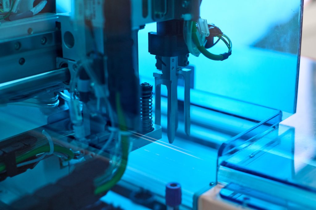
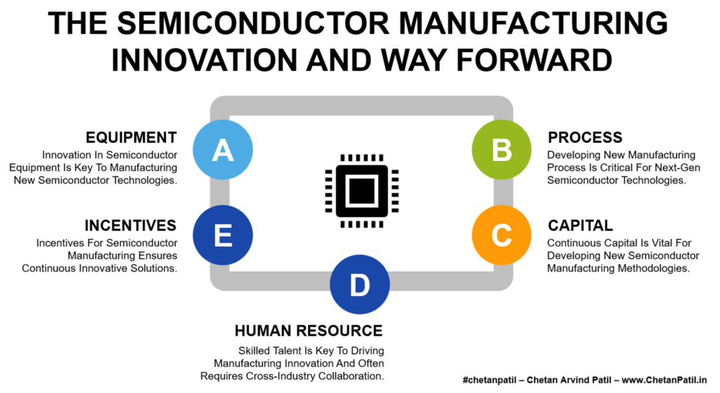
Equipment: Semiconductor equipment is the backbone for semiconductor manufacturing. Different xUV solutions are required to drive next-gen technology nodes and thus require continuous innovation via research and development activities.
Process: Developing processes that can provide the customer with options to power next-gen solution is the need of the hour. These processes can belong to the same technology node or a new technology node/process. Developing, validating, testing, and releasing these processes is crucial for semiconductor manufacturing innovation.
Capital: The semiconductor manufacturing houses need to focus on the customer requirement apart from the future market demand. Both of which require continuous investment. Thus, making new processes development a very capital-intensive task.
The major hurdles in enabling continuous innovating semiconductors are the cost and time. Cost is critical, mainly because the investment does not generate ROI until the technology is fully developed. The time directly impacts the costs. The longer the research is, the higher the time and thus the cost.
Apart from product development, semiconductor manufacturers also have to balance the research and development activities. Not doing both together will make today’s solution irrelevant in the future. And, without the next-gen in-house developed solution available for future use, the long-term impact might not be good.
Apart from the technical details, several business aspects need to be considered for long-term innovation in semiconductor manufacturing.
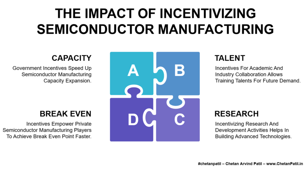
One such critical business part is the human resource required to bring innovative ideas into reality. Unless and until the focus is on correctly training the talent to bring the innovation forward, there is no way semiconductor manufacturing will be ready for the semiconductor industry’s requirement for the next century. Doing so often requires collaborating with the universities to train the students to enable human resources for its future requirement.
Human Resource: Talents with a wide range of skills sets are required for enabling future innovation. It often requires both academia and industry to come together and drive a curriculum that can bring more skilled talent to the semiconductor manufacturing industry.
Incentives: Semiconductor manufacturing itself is a high capital-oriented industry. Semiconductor manufacturers thus do require support from government bodies that can help them balance the product development capital versus the capital needed for research.
Another critical business aspect for continuous innovation in semiconductor manufacturing is the incentive part. It comes directly from the state and/or central/federal bodies. A long-term incentive can empower semiconductor manufacturers with the ability to come up with innovations, and at the same time can lower the burden to invest in existing setups and facilities.
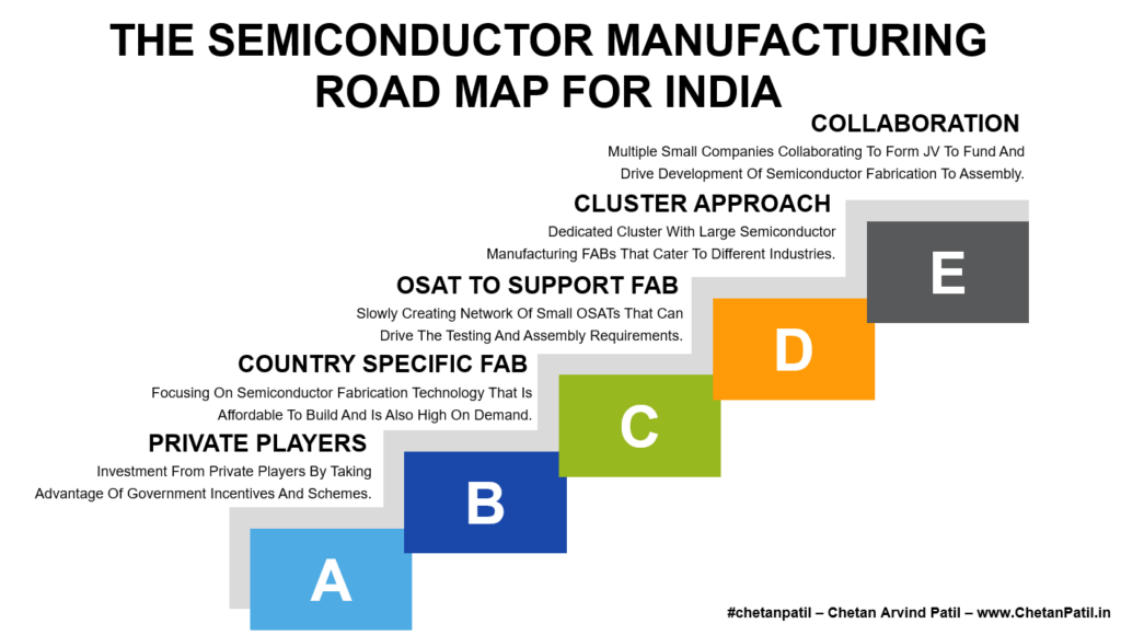
Semiconductor manufacturing is critical from the design and also the manufacturing point of view. A manufacturing house cannot survive without a continuous push for next-gen semiconductor technologies. Doing so also requires support from public bodies, which is also a differentiating factor between the new regions that will grow as the next big destination for end-to-end semiconductor solutions.
The next few years will be crucial for semiconductor manufacturing due to the rush towards providing More-Than-Moore manufacturing solutions. The semiconductor manufacturing companies that have invested in such solutions long back will eventually win the race.