Author: admin

  • The Need To Focus On Outsourced Semiconductor Assembly and Test

    The Need To Focus On Outsourced Semiconductor Assembly and Test

    Photo by Devin Spell on Unsplash


    THE IMPORTANCE OF OUTSOURCED SEMICONDUCTOR ASSEMBLY AND TEST

    Outsourcing is one of the several ways to optimize in-house business activities, and that is why the majority of the industry heavily takes advantage of outsourcing. In the long run, hiring an external vendor to outsource part of the product development process not only brings operational efficiency but also provides an avenue to optimize internal resources.

    The semiconductor industry is also heavily driven by outsourcing. More than the design, the manufacturing aspect of the semiconductor product development relies on services provided by external vendors. The two major examples of semiconductor outsourcing are FABs (Pure-Play Foundries) and OSATs.

    Pure-Play Foundries: Provides services that transform the design files into real silicon wafers.

    OSATs: Takes the silicon wafers fabricated and puts them through the testing process before assembling.

    The semiconductor shortage has shown the world the importance of semiconductor FABs. This is the primary reason why all over the world countries are coming up with attractive incentives to invite the Pure-Play Foundries to set up new FABs. However, from the semiconductor manufacturing point of view, semiconductor FABs provide only 50% of the services that are necessary to turn a product design into reality. The rest of the 50% is dependent on the OSATs – Outsourced Semiconductor Assembly and Test.

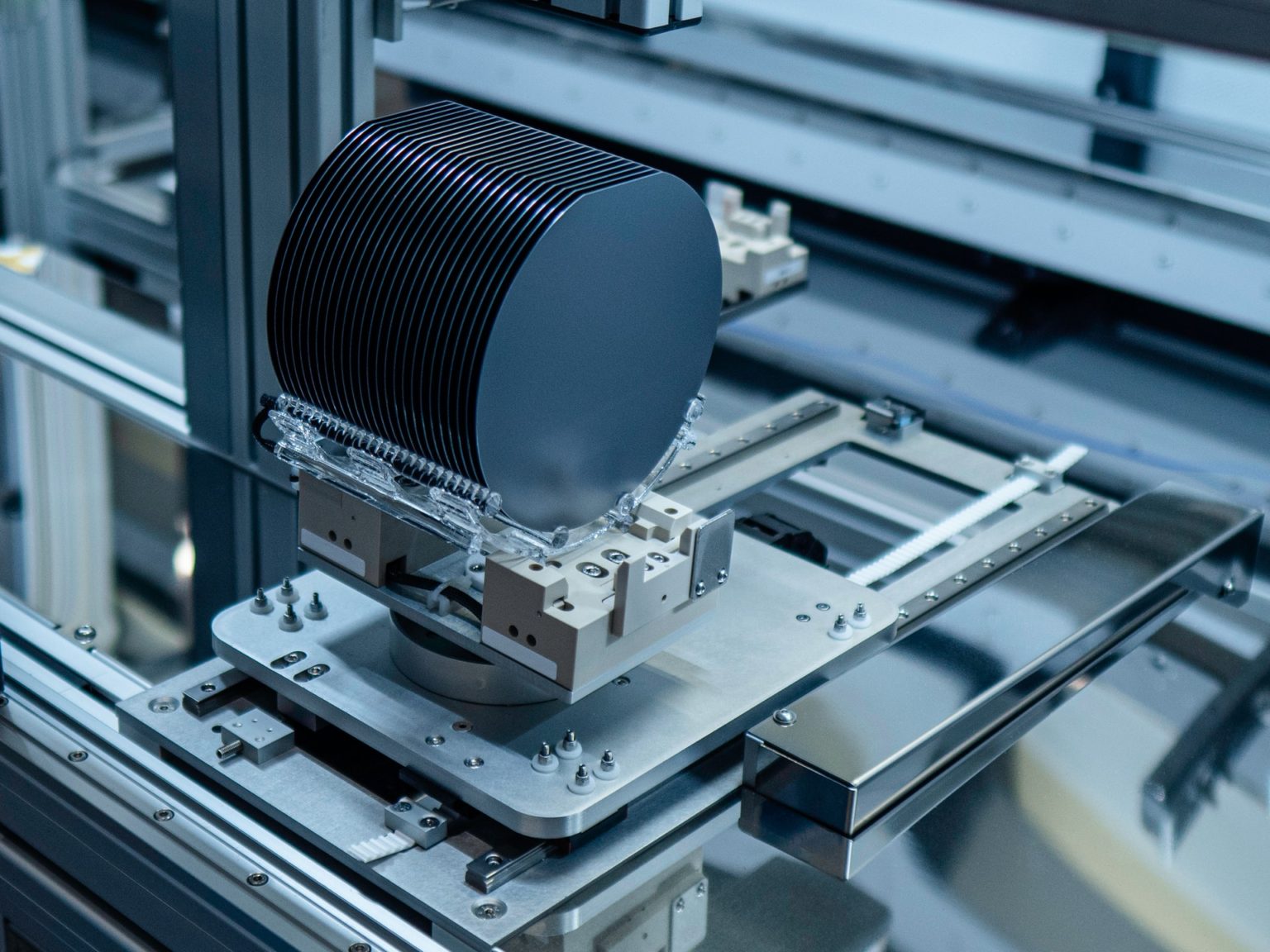
    Test and packaging (also referred to as assembly) is a major part of semiconductor manufacturing, and these two are the services that OSATs provide. OSATs invest heavily in equipment and processes that enable testing of different types of wafers/parts apart from providing high-tech research-driven packaging solutions. The cost associated with running the testing and packaging process is the major reason why the majority of semiconductor companies are relying on outsourcing.

    In doing so, over the last four decades several OSATs have come up all over the world. However, their growing importance is also the major reason why the semiconductor industry should also focus on OSATs when talking about building new manufacturing capacity and not just focus on semiconductor FABs that only provide half of the semiconductor product development process.

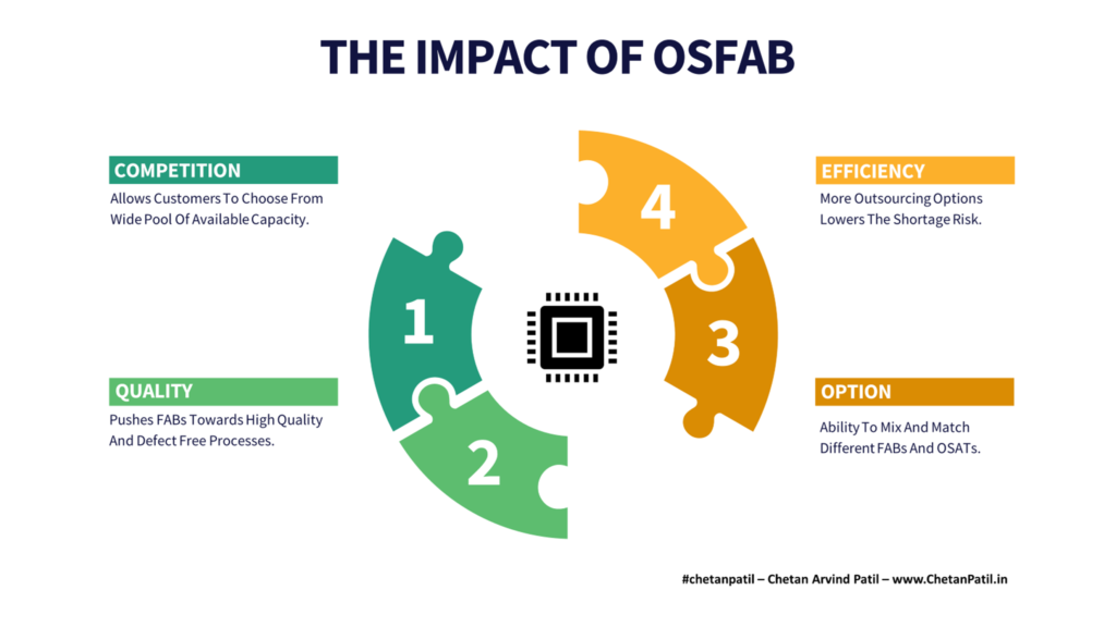
    Several factors have made OSATs the backbone of the semiconductor industry. The semiconductor supply chain will be inefficient without OSAT houses because of the following importance:

    Assembly: Any piece of semiconductor die has to get packaged into an assembled product that can be soldered onto the target application platform. This is where OSATs come into play as their first area of focus is to drive assembly (by providing different package technology) services. OSATs invest heavily in research and development activities to provide different types of assembly options, and over the last few years, semiconductor design houses have also relied on OSAT to drive their assembly requirement.

    Testing: Testing and assembly go hand in hand, and that is why OSATs by default provide testing services. These services require high-end equipment so that any type of wafer can be tested with minimal human interference. In many cases, testing is also carried out on the packaged parts and is a de-facto way to screen bad parts out of the assembly line.

    FAB-LESS/IDM: In the semiconductor industry, not all companies have in-house manufacturing facilities. This is more applicable for FAB-LESS and some IDMs. These two types of companies thus leverage external FABs and OSATs to cater to their need for fabricating, testing, and assembly. This is another reason why OSATs have grown in importance as several FAB-LESS/IDM are dependent on them.

    Quality: Several years of industrial experience have enabled OSATs to provide high-quality services that drive defect-free testing and assembly solutions. In the long run, OSATs ensure that the product being tested and assembled follows a robust recipe that allows them to remove any low-quality part out of the production line thus improving the quality of their customer’s product.

    Supply-Chain: The end-to-end semiconductor flow requires several stakeholders to come together. This is where companies providing different services come into the picture. The design and fabrication houses are a major part of the supply chain. However, the testing and assembly requirement makes the semiconductor supply chain incomplete without OSATs. The outsourcing facilities provided by OSATs make them the last critical step in the semiconductor supply chain.

    Even though there are several OSAT vendors in the market, only a few players are well known and have also expanded their business and reach over the last few decades. While this is certainly good news for the semiconductor growth, but slowly it is presenting a challenge similar to the semiconductor FABs, where a handful of players are driving the semiconductor back-end business. The same scenario is applicable in the OSAT arena, where few companies are increasing their market share and making the semiconductor supply chain dependent on them.

    In the long run, this can prove out to be a costly scenario and that is why the semiconductor industry needs diverse players to provide semiconductor FABs and OSATs services. Today is the right time to do so as countries are looking to attract new manufacturing houses to set up shops and new players can leverage these incentives to create a niche market for themselves.


    Picture By Chetan Arvind Patil

    Picture By Chetan Arvind Patil

    THE OPPORTUNITIES IN THE OUTSOURCED SEMICONDUCTOR ASSEMBLY AND TEST ARENA

    The OSAT market share shows a similar story as the semiconductor FAB. There are three to four players in the OSAT arena that are dominating the market for several years, and year-on-year this gap is increasing when compared to other smaller OSAT players.

    There is certainly nothing wrong if the big OSAT players are getting bigger. The problem arises when there is a spike in demand and the top players are not able to accommodate all the requests, which eventually leads to higher processing (test and assembly) time. In situations like these, the need for larger diversified OSAT capacity is felt.

    The sudden rise in semiconductor demand has not only affected the semiconductor FABs but has certainly also affected OSATs. In some sense, this presents an opportunity for emerging OSATs, semiconductor investors, and also countries/governments to focus on OSAT business if the cost of developing new FABs is too high/risky.

    OSATs can be an excellent vehicle for emerging semiconductor manufacturing regions as they require less investment compared to semiconductor FABs and on other hand, the revenue is attractive too. Focusing on OSAT capacity improvement can also drive growth in semiconductor manufacturing for countries that haven’t had the fortune of housing semiconductor FABs so far.

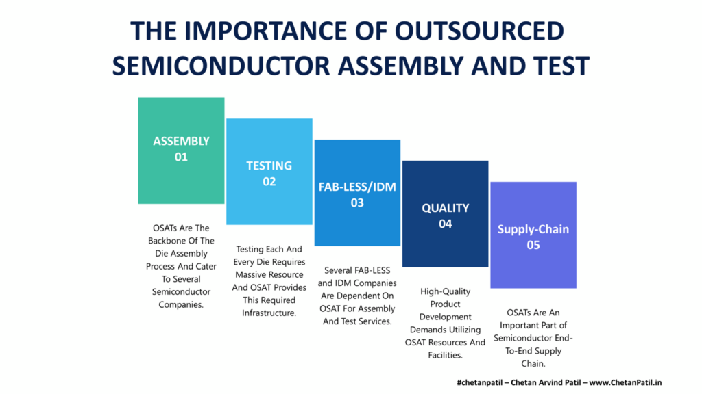
    The opportunities presented by the OSAT business arena are many and are a good mix of business and technical dependency:

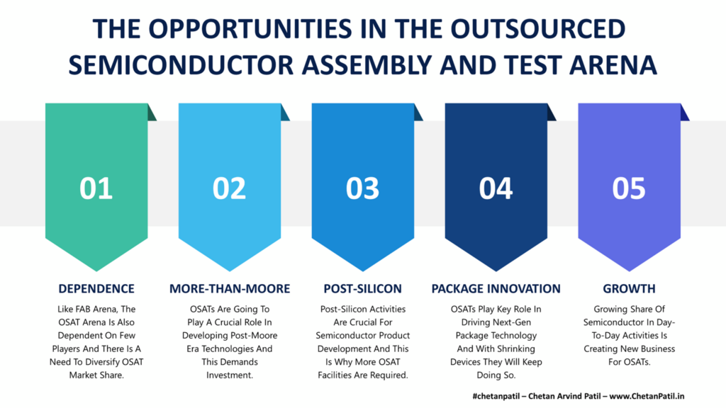
    Dependence: When it comes to optimizing semiconductor operational activities, hiring OSATs to perform semiconductor testing and packaging is the most important decision. The growing dependence on OSAT has lead to the expansion of some of the top players and this is making FAB-LESS to IDMs dependent on few top OSAT houses. To balance this out (similar to what the semiconductor FAB market also needs) there is an opportunity for new emerging OSAT to provide more capacity to the semiconductor industry and this might ensure that there is no dependence on few select players.

    More-Than-Moore: As the world move beyond 1nm, the research around technologies that can drive solution beyond Moore’s law is also critical. OSATs have an important part to play, and the major reason is due to the different types of package technologies that can help drive next-gen semiconductor solutions like chiplets and heterogeneous integration.

    Post-Silicon: More than 50% of the semiconductor product development activities occur during the post-silicon stage. From FABs to OSATs to ATMPs to Distributers, all play a critical role in bringing the design to life. As part of the post-silicon process, OSATs have increased their importance over the last decade. The complexity brought by the new chip design is also pushing OSATs to upgrade their facilities to handle the probing of new types of chips. This presents an opportunity not only to the OSAT market but also to the equipment and tool manufacturers.

    Package Innovation: Innovative package solutions will be a continuous development process. FAB-LESS and other types of semiconductor design houses can come up with new packaging solutions, but they will always require an OSAT vendor to execute and bring the new package technology to reality. The major reason is the lack of internal or in-house assembly and testing facilities (which often require millions of dollars), and relying on OSAT is the best way to optimize the cost while driving new package innovations.

    Growth: The increasing share of semiconductors in day-to-day solutions is putting a lot of pressure on semiconductor manufacturing. This is the major reason why for the next few years or even decades, the semiconductor market will keep growing. The heavy dependence on OSAT services makes them a perfect venture to be in, and also makes them a great candidate for countries looking to ignite semiconductor manufacturing clusters within their borders.

    The importance of OSAT is well known in the semiconductor industry. They provide critical services by building larger facilities that can drive the last important piece of semiconductor manufacturing. This is why countries looking to attract semiconductor manufacturing houses should focus on OSATs and then build the semiconductor manufacturing infrastructure up to the FABs.

    Ultimately, as the importance of manufacturing aspect of the semiconductor product development grows, the importance of both the FABs and OSATs will grow too.


  • The Evolving Semiconductor Wafer Size

    The Evolving Semiconductor Wafer Size

    Photo by Maxence Pira on Unsplash


    THE IMPACT OF WAFER SIZE ON SEMICONDUCTOR INDUSTRY

    The semiconductor industry is built on the platform laid by silicon wafers that form the base of fabricating different types of advanced semiconductor products. The silicon wafers have gone through an incremental change in size/diameter over the last half-century. The growing need for advanced semiconductor products is now raising another round of discussion to move beyond wafer size in use today, mainly as a factor to improve the production rate of new semiconductor FABs and OSATs.

    The semiconductor manufacturing facilities around the globe are categorized based on the wafer size they can handle. The majority of the FABs and OSATs today are focused on 200 mm (7.9/8 inch) wafers with a few focusing on 300 mm (11.8/12 inch). On other hand, only small FABs and OSATs cater to 150 mm (5.9/6 inch) wafers.

    Wafer size plays a crucial role in deciding how the FABs and OSATs are built. The major reason is the equipment and tools that are required vary based on the wafer size and with the increase in wafer size the cost of setting up new FABs and OSATs increases too. This is why selecting the right wafer size a crucial.

    Eventually, the choice of wafer size is more investment and strategically driven rather than technical. The reason for this is the impact of any change in wafer size on the full end-to-end semiconductor flow.

    Wafer Size: Larger wafer size certainly provides more die per unit area. The extra area to fabricate more die eventually allows FABs and OSATs to fabricate and test/assemble more dies in a given time. This pushes the rate at which new products can be fabricated/assembled and to some extent increasing wafer size can also have a positive impact on the supply chain.

    Die Per Wafer: Wafer size clearly defines how many die per wafer there will be. This allows the semiconductor design houses to gauge how much cost savings will be there. In the end, a smaller wafer for a high demanding product will lead to more wafer orders compared to a relatively larger size wafer. This balancing act is the major reason why companies often have to spend more time analyzing the pros and costs of selecting wafers from the business perspective.

    Cost: Wafer size certainly dominates the cost of developing a semiconductor product. Apart from the cost of the wafer itself, there are FAB and OSAT costs that also need to be considered. Using a 200 mm (7.9/8 inch) wafer will certainly have a lower cost of fabricating and assembling semiconductor chips compared to a 300 mm (11.8/12 inch) wafer. In the end, it is all about creating the margin by selecting the right wafer size.

    Yield: Historically, as the wafer size has increased the yield has come down. A product fabricated on a 300 mm (11.8/12 inch) wafer will have a lower yield compared to the same product on a 200 mm (7.9/8 inch) wafer. In the end, the final yield will be comparable, but the loss of yield as the wafer increases is mainly due to the time required to perfect the semiconductor process, which improves as more products use the same wafer size as the learnings can be captured and applied to improve overall product yield. Wafer handling also plays a crucial role in deciding the final yield and as the wafer size increases, it becomes difficult to lower the number of process steps due to a large number of die per given area.

    Process: Wafer size is so crucial that semiconductor manufacturing facilities have to play a very long game and decide upfront the wafer size they will support over the next 5 to 10 years. The major factor is the cost associated with the process that is required to set up based on any upgrade in wafer size. To play safe, the majority of the semiconductor facilities have zeroed on to 200 mm (7.9/8 inch) wafer as they allow the balance of both the technical and business aspect. However, the need for 300 mm (11.8/12 inch) is putting pressure on FABs and OSATs to go for upgrades.

    The above points clearly show the impact wafer size has on a different aspect of the semiconductor process. From cost to yield, there are several things to consider when the time comes to decide on which wafer size will be used to produce the next-gen product.

    In the end, the decision is taken by the semiconductor houses who design and own the chip as the manufacturing facilities are only providing services.


    Picture By Chetan Arvind Patil

    Picture By Chetan Arvind Patil

    THE STEPS TOWARDS NEW WAFER SIZE FOR SEMICONDUCTOR INDUSTRY

    The current saga of semiconductor shortage is also raising the question of going a setup further and reigniting the discussion of going for the largest wafer size (300 mm (11.8/12 inch)) in production today.

    This means pushing all the to-be-designed FABs/OSATs capacity to opt for 300 mm (11.8/12 inch) or even 450 mm (17.7/18 inch), which has not been used for full fledge production so far. The major argument is to increase the capacity per FAB/OSAT by equipping them with the process to churn more die per unit area. This will certainly require huge investment and not many FAB/OSAT will be willing to opt for anything more than a 200 mm (7.9/8 inch) wafer.

    However, the semiconductor industry should also take a look at the wafer size from the growing dependency on semiconductor products. The most efficient way to eliminate any future demand that leads to the shortage is not only to build more FABs/OSATs but to also equip these facilities for future needs.

    Even if the FABs/OSATs are initially designed and equipped with a 200 mm (7.9/8 inch) or 300 mm (11.8/12 inch) wafer, they should also start planning for 450 mm (17.7/18 inch) today. Following such a strategy will allow FABs/OSATs to be ready for the future demand that can certainly exceed the total capacity that will be available in the near term.

    There are robust steps required to drive the adoption of a much larger (mainly 450 mm (17.7/18 inch)) wafer size than that is produced today, and the below roadmap provides a holistic view of why different steps should be taken towards larger wafer size.

    Capacity: Today’s capacity is built on top of different wafer sizes and certainly it is not enough as per the semiconductor shortage. Building more FABs/OSATs will certainly provide higher capacity but not as much when the wafer size is increased. The semiconductor manufacturing houses need to take a long-term look at what is the loss of not upgrading to higher wafer size. It can start with 300 mm (11.8/12 inch) wafer FABs/OSATs and then move towards 450 mm (17.7/18 inch).

    Collaboration: Setting up FABs/OSATs that can handle larger wafer sizes is costly. The only way to mitigate this cost is to bring different manufacturers together and invest in cluster-based facilities that cater to different customers. This will certainly invite IP and other confidentially issues but without a collaborative approach, it is not possible to increase capacity that is focused on larger wafer (300 mm (11.8/12 inch) or 450 mm (17.7/18 inch)) size.

    FAB-LITE: Another approach towards handling wafer size can be to create a few niche semiconductor FABs and OSATs that only cater to future large wafer sizes. These can be facilities that are focused on 450 mm (17.7/18 inch) or 675 mm (26.6/27 inch) wafer FABs/OSATs. This strategy will make these new facilities the future R&D places that can drive the development of larger wafer size and as the technology progresses the lower cost of utilizing these larger wafer size will lead to mass production.

    Target Node: Larger wafer size can also be used for specific technology-nodes. This way the cost of production can also be balanced along with the investment required. The best suitable nodes can be older nodes that have a more robust process than the future new technology-nodes. This can certainly help drive the adoption of higher wafer size too.

    Efficiency: In the end, larger wafer sizes bring efficiency by shipping more parts in the same amount of time. The overall cost and investment will balance (as long as the production technology is affordable) out. This is another reason why the semiconductor industry should move towards a larger wafer size.

    The steps if taken strategically can re-ignite the discussion of bringing 450 mm (17.7/18 inch) wafer into production and can certainly create a niche network of FABs and OSATs that can ramp up the production by providing more die per area (not just wafer but also facility area).

    The semiconductor industry has to capture the cost of creating hundreds of FABs/OSATs versus a handful of high capacity FABs/OSATs that can handle much larger wafer sizes than today and thus providing a way to balance the cost and capacity for future demands.


  • The Semiconductor Chips For Data Centers

    The Semiconductor Chips For Data Centers

    Photo by Taylor Vick on Unsplash


    THE BUILDING BLOCKS OF SEMICONDUCTOR CHIPS FOR DATA CENTERS

    The connected world is leading to real-time information exchange, and this is why consumers to enterprises expect the request to be processed in the fastest time possible. The devices used to send such requests can only process and store a certain amount of data. Anything beyond a threshold requires the use of data centers, and that also means transferring/receiving data over the air.

    The computing industry has relied on data centers since mainframe days. However, the importance of data centers has mainly grown due to the connected systems. These data centers have to run 24×7 and also have to cater to numerous requests simultaneously.

    To ensure a quick and real-time response from data centers, three major systems have to work in synchronization:

    Software: If a smartphone user is sending the request, then the data needs to be encrypted in packets before sending it over the air to the remote location where the massive data centers are located. This means the software solutions, both on the client and the server-side, have to work in harmony. This is why software is the first major system required for accurate data center operation.

    Connection: The second major system is the network of wired and wireless systems that aid the transmission of data from the client to the server (data centers). If a robust connection is not available then data centers will be of no use.

    Hardware: The third and most critical piece is the silicon chip or hardware that makes up the data center. These tiny semiconductor chips end up catering to all the request that comes from different part of the world. To ensure the request is fulfilled in real-time, a smart silicon chip is also required that can handle the data-efficient without adding bottlenecks.

    The growing internet user base along with data-driven computing solutions has to lead to the high demand for data centers. To cater to all such growing services, different types of data centers are required. Some data centers are small in size (less number of servers) and some are giant. Data centers with more than 5000 servers are also called hyperscale data centers. In 2020, there were more than 500 hyperscale data centers running 24×7 and were catering to request coming from any part of the world.

    Data Centers Require Different Types Of Semiconductor Chips.

    To run these hyperscale data centers requires large facilities, but the key piece is still the tiny semiconductor chips that have to run all the time to handle different types of requests. Due to the growing focus on data centers, there is a need to change the way new semiconductor chips are being designed for data center usage.

    This is why all the semiconductor chip solutions that end up getting used in the data centers should be built around the following blocks:

    Processing: Semiconductor chips for data centers should be designed to process not only a large amount of data but also a new type of data. This requires designing semiconductor chips that can cater to the request in the shortest time possible, while also ensuring there are no errors during the processing.

    Security: Data centers receive different types of data processing requests and this data can have any information from credit card processing requests to personal information to login credentials. Semiconductor products by default have to focus on the security aspect when designing silicon solutions for data center usage.

    Workloads: Rapid software development has lead to different types of data. Data eventually lead to the formation of workloads that the computing system has to process. Given the rise of AI/ML/DL, there is a need to process the data elegantly. This requires doing away with traditional processing blocks and instead of adapting to more workload-centric architecture that can enable a high level of parallelism to train and infer information out of it.

    Adaptive: Smart world not only requires data capturing but also demands adaptive decisions. This often requires on-the-go training and modeling to ensure the user request is fulfilled intuitively. This is why there is a demand to drive AI drive architectures that can train data efficiently (eFPGA or NPU) and ensure any new (and never seen) request is handled without errors.

    Storage: Memory is one of the major building blocks of the computing world. The surge in the use of cloud storage is leading to new innovative storage systems that can provide more storage per dollar. This requires driving new semiconductor solutions so that data centers become powerful but at the same time are compact enough to not consume a large amount of energy.

    Efficiency: Data centers are considered to be one of the most power-hungry systems in the world. The year-on-year growth in hyperscale data centers is only going to increase the power consumption. To balance the processing need with the power consumption, semiconductor solutions have to consider the energy consumption per user request. By building an efficient semiconductor chip, the data centers can expand in number without impact the total power consumption.

    The above building blocks are not specific to XPUs for data centers only. These blocks are valid for another type of semiconductor chip that data centers require. This can be a networking solution (PCIe) or a new data transfer (HBM) interface. Eventually, the above points discussed are the major reasons why data centers require different types of semiconductor chips.


    Picture By Chetan Arvind Patil

    Picture By Chetan Arvind Patil

    THE BOTTLENECKS TO DRIVE NEXT-GEN SEMICONDUCTOR CHIPS FOR DATA CENTERS

    Designing and manufacturing semiconductor chips for any type of solution requires a thorough understanding of different issues and opportunities. The same strategy is applicable when coming up with semiconductor solutions for data centers. For data centers, the complexity is much more than consumer systems mainly due to the need to provide bottleneck-free semiconductor products that run all the time.

    Over the past few years, new data center-focused semiconductor companies have emerged and they have been providing different solutions. Fungible’s Data Processing Unit and Ampere’s ARM-powered XPU are a couple of such examples. However, in the end, the goal of all the semiconductor solutions is to focus on a set of features that ensures all the request is catered by the data centers in the real-time without adding any bottlenecks.

    When it comes to bottlenecks in the world of computing, the list is endless. These bottlenecks can originate either from software or hardware. Eventually, the software features have to be mapped onto the hardware so that both software and hardware can work in synchronization to drive next-gen solutions.

    The next-gen semiconductor chips need to focus on a few criteria’s to drive bottleneck free semiconductor powered data centers:

    Features: Traditional semiconductor chips for data centers were (and still are) purely focused on performance. As the world is increasingly adopting connected systems, there is growing demand to balance performance with efficiency. This requires a new set of features that can ensure that tomorrow’s data centers are more efficient than today’s. These features can range from using advanced transistor-level techniques to new packaging solutions.

    Data: The amount of data that hyperscale data centers have to crunch will keep increasing every year. The storage aspect of it will also grow along with it. This growth is leading to huge cooling systems and thus adds to total energy requirements. This challenge of managing data while lowering the impact on power consumption is pushing new solutions. More modular approaches are needed to drive next-gen semiconductor solutions.

    Parallelism: Any given chip of any type in a data center can receive any amount of request. To ensure there are no bottlenecks, intelligent parallelism techniques are required. Some of the parallelism techniques require software support but many often do require hardware features (cache, data pipeline, etc.) that can support parallelism. Networking and XPUs solutions often have to consider this problem while designing chips for data centers.

    Speed: While there is a growing concern of power consumption (by data centers) due to performance requirements, there is also demand to drive faster response out of data centers. This requires designing semiconductor chips for faster processing. Balancing the power, performance, and area aspect for data centers is becoming more difficult than ever. This is leading to more modular data centers but it is still going to demand semiconductor chips that can provide a high-speed solution without adding to the power requirement.

    Network: Data centers have to communicate with different systems that are located in remote areas, and such communication requires heavy usage of networking solutions. To drive communication efficiently, robust networking chips are required that can handle the data without any errors. This demands designing and manufacturing semiconductor solutions with reliability and error correction. In the long run, network chips are going to play a vital role and require the bottleneck-free design to drive new data centers.

    Architecture: Intel is considered the leader in XPU solutions for data centers. To design XPUs, Intel has been relying on its homegrown x86 architecture. In the last decade, the emerging workloads have changed a lot and that requires new XPU solutions. To provide newer solutions, emerging companies are focusing more on ARM and RISC-V to power their solutions. The major driving factor to use ARM or RISC-V is the ability to adapt and change the architecture to suit future requirements. Picking up the architecture is vital to avoid any kind of bottlenecks in the XPUs for next-gen data centers.

    In the last two years, the world has moved towards data center solutions mainly due to the remote feature required by different services. The growth in the number of smartphone and smart device users is also driving the need for new and efficient hyperscale data centers. To cater to the future demand of green hyperscale data centers, the existing and emerging semiconductor companies will keep coming up with a newer solution.

    In the long run, newer data-centric semiconductor solutions are only going to benefit the computing industry and the race to wind data centers has just begun.


  • The In-House Custom Semiconductor Chip Development

    The In-House Custom Semiconductor Chip Development

    Photo by Jason Leung on Unsplash


    THE REASONS TO DEVELOP CUSTOM SEMICONDUCTOR CHIP IN-HOUSE

    As technology is progressing and touching every aspect of day-to-day life, the dependence on semiconductor solutions is also growing. These solutions are often made by semiconductor companies and can power several things from sensors to a smartphone to cars to satellites to name a few.

    One of the most critical infrastructures that the semiconductor industry powers are data centers and portable computing systems. These two systems are interconnected as one cannot do without the other. Today, majority of the request a smartphone users sends ends up in one of the numerous data centers around the world. The data centers then quickly crunch the request and send it back to the requesting user. As the customer base and internet users grow, there is a surge in demand for power-efficient computing systems (both data centers and portable computing systems) by the software or data-driven companies/industry.

    Data-Driven Industry Is Getting Into Custom Semiconductor Chip Development

    The big software and data crunching companies are often dependent on specific semiconductor solution providers who have been powering their data centers and portable computing systems for decades. The silicon chip these semiconductor companies design often falls in the category of the general-purpose chip, so the same is used by different customers even though their requirements might differ. So far, general-purpose strategy has worked wonders. However, as the software industry explodes (due to data), the big giants are realizing the importance of powering their data centers (and in some cases portable computing systems too) by developing custom chips in-house.

    This change in landscape is mainly because the data crunching companies understand the need, purpose, and features that they require to drive bottleneck-free solutions for their customer. This can only be possible by starting chip development in-house so that software companies can deploy custom chip solutions across their data centers to drive services more efficiently. This is evident from the fact that YouTube has deployed its chip for video transcoding for faster processing of videos, and even Microsoft’s Pluton secure chip solution for its Windows platform.

    While providing better solutions is certainly the main goal of developing the custom chip, there are several other reasons too. All these reasons ensure the in-house chip development by non-semiconductor companies is a win-win idea or not.

    Cost: One of the major driving factors of developing chips in-house (at lead the designing part) is the cost. Having control over what chip needs to be designed and how to deploy it (as per the features) can potentially enrich user experience while bringing in savings. Savings are captured mainly in the form of usage when different computing systems within the company start utilizing the custom solutions. In many cases, the benefits can also be gauged based on how much power savings are achieved (data centers) compared to the traditional outsourced general-purpose solution.

    Time-To-Market: Another benefit of designing custom semiconductor chips is for companies whose end product is a smart solution. This can range from kitchen appliances to television to desktops and many more. Having the ability to design and create chips in-house can allow greater control over launching products and takes away the uncertainty that general-purpose solutions provide. This is very true for data centers that heavily rely on x86 architecture solutions to drive future data centers.

    Flexibility: Software changes very quickly and can demand new features out of the silicon chip. If there is no in-house development, then all these requests will eventually have to go out of the company in form of outsourcing. If there is a dedicated silicon development in-house team, then the software team can work in collaboration with the internal team (safeguarding IPs) to drive better hardware-software systems to power emerging solutions.

    Features: If a company is selling laptops and relies on an outside vendor for chip development, then it makes them vulnerable due to dependency. Incorporating chip development in-house can provide a way to balance the chip requirement that can drive better systems. This can also push outside vendors to bring new features and in the long term, the competition helps the industry at large.

    Applications: Developing in-house semiconductor chips can also provide avenues to expand the application area. This can be very true for smart device providers who often have to build systems based on what is available in the market. In-house chip development activities if planned well can allow companies to expand their portfolios by driving new end-products for their customers.

    Dependency: Companies that are into data centers are heavily dependent on different companies for silicon chips to power their systems. Many of these solutions are not specifically designed to cater to everyone procuring the company’s request. This makes the data center companies heavily reliant on external factors to driven in-house innovation which today certainly requires custom chips.

    All of the above reasons are the driving factor that is pushing several big software companies to drive in-house semiconductor chip development plan.

    It is also true that not all companies have the need or focus to create such custom solutions. But in the long run, as the dependency on the silicon chip grows, the risk associated with not developing an in-house semiconductor chip might be far greater than not planning for it.


    Picture By Chetan Arvind Patil

    Picture By Chetan Arvind Patil

    THE REQUIREMENTS TO DEVELOP CUSTOM SEMICONDUCTOR CHIP IN-HOUSE

    Developing semiconductor solutions is not an easy task. Even for big software giants, it has taken years of planning and execution to come to a stage where they can deploy custom in-house developed silicon solutions across data centers and portable computing systems. This is why it is important to understand the different requirements that are the driving factor in ensuring the in-house semiconductor chip is impactful and profitable at the same time.

    In-house silicon chip development requirements do take time to execute and often require tons of resources apart from the time it takes to perfect a semiconductor chip solution.

    Team: The most important criteria for developing a successful in-house chip is to ensure that there is a team with an excellent set of skills to execute custom chip development flawlessly. The team often has to be a combination of excellent design and manufacturing skills. This means hiring individuals who have been in the semiconductor industry for a long time and are capable of developing semiconductor solutions via long-term research and development. A dedicated manufacturing team is also critical to bring ideas to life.

    Acquisition: The team is one part of the development of in-house silicon chips. Another part is the ability to ensure that the company can acquire outside assets (IPs and patents) as and when required. This greatly pushes the in-house development activity in a positive direction and many cases reduce the efforts required to bring in-house silicon chip development to reality.

    Investment: Managing teams, labs, and other resources often require a massive amount of money. If a company without a semiconductor background is entering in-house chip development activity, then the company should ensure there is a large amount of investment available for a very long time. This is why it is important to ensure that over the long period of chip development process and research, the investment activity will pay off in the long run.

    Roadmap: In-house chip development also means having a clear strategy as to why the company should do it. Having teams and resources to tackle one specific feature without a plan is not a good strategy to invest time and money behind in-house chip development. Major emphasis should be on the long-term plan and how it will benefit the company. This often requires a clear roadmap is a must-have requirement.

    Balance: Not all semiconductor solutions require in-house development, and that is why it is very important to balance the focus in terms of what part of the silicon requirement should be outsourced and which is worth developing in-house. It is not possible for software or data-driven companies to become full-fledge semiconductor solution providers overnight and no single company (even core semiconductor) develops everything in-house. This is why a filtering mechanism of balancing the in-house and outsourcing is important.

    Bottlenecks: Major criteria of in-house development of silicon chip is also to remove any barrier in developing new products. The roadmap should allow bottleneck-free development of in-house semiconductor products as long they meet the company’s requirements.

    The reasons and requirements showcase how and when the non-semiconductor companies should get into the semiconductor design segment. In-house semiconductor development has already started long back and many of the companies (Google, Microsoft, and Amazon to name a few) have already enjoyed success around it. The major reason for doing so has been the greater control of designing features that in reality removes the issues the companies were facing.

    This trend of taking things in hand and designing solutions in-house is certainly going to continue, more so due to the semiconductor shortage and the impact it had on several industries.


  • The More-Than-Moore Semiconductor Roadmap

    The More-Than-Moore Semiconductor Roadmap

    Photo by Jeremy Zero on Unsplash


    THE BUILDING BLOCKS OF SEMICONDUCTOR ROADMAP

    The semiconductor industry has enjoyed the success of doubling (every two years) the number of transistors in a silicon chip, which has allowed semiconductor companies worldwide, to offer novel semiconductor products and solutions. This is exactly what Moore’s law predicted when it was proposed around four decades ago.

    Increasing transistor density per given area allows computer systems to cater to multiple (and numerous too) requests at the same time. This is why in 2021 a smartphone is capable of crunching the data that in the 1980s would require a giant server.

    However, as the semiconductor world marches towards 3nm mass production (with 2nm already showcased by IBM), there is a growing concern about whether or not Moore’s law will keep pace with the advancement in the technology-node (mainly shrinking transistor size) and what are the alternate solutions.

    More-Than-Moore Solutions Have Been In Work For Last Two Decades.

    The answer to this problem lies in the different unique solutions that the semiconductor industry has been working around in the last couple of decades. The semiconductor industry knew there is going to be a time when Moore’s law will not be applicable as it is today and a course correction would be needed.

    This course correction has led to numerous design to manufacturing changes that have enabled silicon chips to provide more performance and better power consumption without compromising on the area. These solutions have been built on top of different semiconductor product development processes which have come together to drive next-gen workloads without worrying about the future implications of Moore’s law.

    Design: To drive innovative solutions that defy Moore’s law by providing similar/better performance and lower power consumption often requires a novel design. These designs can at the circuit level or the system level. The combination of both enables richer design solutions. Like AMD’s chipset-based CPU and GPU design or Appel’s M1 SoC. All these design methodologies drives next-gen solutions that are needed to run future workloads optimally. Such designs often require years of research and development that leads to patents and IP. TVS is another design solution that has allowed novel chip designs.

    Node: When it comes to choosing a technology-node for a high-performance device like XPU, the choice is always to go for the best out in the market. This is why companies like TSMC, Samsung, IBM, and Intel are racing to provide the most advanced solution possible. However, the base of the technology-node is a transistor, and to drive a next-gen technology-node that packs more transistor than its predecessor, requires alternate (and better) FET solutions. This is why new scaling CMOS solutions by leveraging new FETs designs is being explored. This started with MBCFETs and soon will move towards forksheet based FETs.

    Memory: To drive data-driven workloads efficiently, memory plays a crucial role. As the design changes to accommodate More-Than-Moore solutions, the memory organization and interface also need to change. This has lead companies like Samsung to come up with High Bandwidth Memory (HBM) to power next-gen AI processing solutions. Similarly, Micron has come up with alternate solutions called HBM2E. Advancement in-memory solutions are vital to ensure any Moore-alternate solutions to drive chips are backed up by faster data processing and data transfer.

    Package: Silicon chip is nothing but a die from a wafer that gets packaged before being mounted onto the application system. With Moore’s law the internals of the chip was doubling (transistor mainly) to enable more performance, and this has to lead to alternate package technology over the years. This can range from WLCSP to WLFO and beyond. Even the new design methodology of chiplets has to lead to alternate package technology from companies like TSMC, which came up with Chip-on-Wafer-on-Substrate (CoWoS), a 2.5D based package technology to drive next-gen chiplets solutions. To keep up with More-Than-Moore, new package technologies will keep coming out in the market.

    Interconnect: As the number of blocks and processing units inside a given chip increases, the need to transfer data faster from one point of the chip to another has also increases. This is why researchers and several companies are focusing on photonics as an alternate. This can ensure the data is not only transferred without adding bottlenecks but also makes sure there is no loss of data. All this while not increasing the power consumption.

    Manufacturing: In the end, all design to interconnect process boils down to the fact that whether the solution is manufacturable. New design process and solutions often require close interaction with the equipment manufacturers, FABs and OSATs. This is why, based on years of development, the semiconductor manufacturing industry is moving towards EUV to drive next-gen manufacturing capability. This is going to not only enable 3nm/2nm technology-node but will also drive different package and interconnect solution that have been proposed in the last few years.

    Different methodologies discussed above have enabled alternate solutions that leverage Moore’s law but by adapting the new design and manufacturing strategies that ensure there are no bottlenecks.

    These solutions range from having a compact chip with all the possible processing blocks to solutions where processing blocks are taken out of the chip and spread across the system. Some solutions also take a different approach of stacking the silicon in such a way that the best of 2D and 3D chip designing comes together to provide a rich user experience.

    All these solutions combined are leading the semiconductor industry towards a Moore-Than-Moore world.


    THE MORE-THAN-MOORE SEMICONDUCTOR ROADMAP

    The semiconductor industry has implemented several solutions that can be considered as an alternate to Moore’s law and also have been around for many years. These alternate solutions focus on how the design and manufacturing process should be handled to ensure there is always a way to drive more power out of the given silicon chip. All these solutions have been designed without focusing much on the transistor density or technology-node.

    It will not be wrong to say that in doing so the semiconductor industry has created itself a pathway to drive into the More-Than-Moore world.

    Below are the four major milestones in the last couple of decades that have established the roadmap for the More-Than-Moore world. Few of these have been known to the semiconductor industry for a very long time and little emphasis has been given as to whether this design and manufacturing solution can provide a path towards More-Than Moore or not. In reality, the solution indeed provides a way after Moore’s law ends.

    System-On-A-Chip – SOC: SOCs have been around for a couple of decades. The need for multi-core systems coupled with graphics, audio, and video processing lead to SOC. SOC allowed different sub-blocks to reside on a single die area and provided a strong challenge to semiconductor designers and manufacturers. The first major reason was the complexity involved in ensuring the design works as expected and the second reason was the ability to produce high-yielding wafers. SOC has had a mix of both the best and the worst of the semiconductor product development process. Some solutions have to see the end of a life well before the planned date and on another hand, some SOC solutions lasted more than their life span. In the end, SOC provided a way to club complex and required solutions in the smallest area with the help of shrinking transistor size. However, this can only last till the power and thermal profile of the solutions makes technical sense and with challenging process development (shrinking transistor size), SOC may not survive the marking for long but during their time allowed a way to club different features under the same die area.

    Multi-Chip Modules – MCM: MCM is a step ahead of SOC. It borrows all the ideas of SOC but brings different types of SOC together on a single platform. The communication between different SOC or ICs is then established using the high-speed interface. This has enabled several XPU (Xeons to Ryzen) based solutions that can diversify the design and manufacturing of the blocks and then leverage interface technology to ensure the data communication is as good or at-par with SOC solutions. Many argue that chiplets design is one form of MCM and in the last couple of years chiplets have taken over the SOC world, and MCM is considered to be the true step towards the More-Than-Moore world.

    System-In-A-Package – SIP: SIP takes the best of MCM and SOC to come up with chip solutions that allow 3D-based stacking of different blocks. The interposer or TVS has played a pivotal role in enabling SIP. The goal of SIP is to take the 2D area and covert it into 3D by stacking the different blocks of SOC/MCM on top of each other. This way the area consumption decreases which 2D solutions like SOC and MCM cannot achieve without using advanced technology-node. SIP does have a drawback as they suffer from thermal and packaging challenges. With advanced technology-node nearing 1nm, SIP might be the best More-Than-Moore solution to provide an alternative to chip designing compared to MCM and SOC.

    System-On-Package – SOP: All the above three More-Than-Moore alternate solutions are designed with the focus that the end system is going to be printed circuit board on top of which the SOC/MCM/SIP system will reside. However, this does not help the smaller devices like smartphones where the goal is to ensure that there is more room for battery by shrinking the board area. To shrink the board footprint, SOP is the best way to design a computing system. SOP takes different chips (either a SOC, MCM, or SIP) and then brings all these individual chips inside a single package. The complexity to achieve an elegant SOP system is way too high. It requires not only synchronization of different types of system/devices (SOC/MCM/SIP) but also a standard interface that can allow packaging of all devices while ensuring that there is no bottleneck or leakage. SOP if done correctly might very well end the need for board and allow a more compact silicon solution while defying Moore’s law.

    The above four semiconductor design and manufacturing alternatives certainly provide a way to design chips (mainly XPU) such that there is no need to worry about packing more transistors in the smallest area.

    From SoC to SOP, the solutions simply take the silicon area out of the context by bringing different sub-systems together but in a unique way, and it pushes the FABs and OSATs to come up with manufacturing technologies (which many FABs and OSATs already have) that can ensure the sub-systems work seamlessly even though there are disaggregated.

    As the semiconductor industry inches towards 1nm technology-node, SOC/MCM/SIP/SOP based chip solutions are certainly going to provide a roadmap for More-Than-Moore solutions.


  • The Reasons And Mitigation Plan For Semiconductor Shortage

    The Reasons And Mitigation Plan For Semiconductor Shortage

    Photo by Marc PEZIN on Unsplash


    THE REASONS FOR SEMICONDUCTOR SHORTAGE

    In today’s market, the majority of the consumer and enterprise products are heavily equipped with semiconductor products (silicon chips). Over the last few years, the share of semiconductors in modern products has increased steadily. From automotive to smartphone to smart devices to aerospace, everywhere semiconductors are present. This has made semiconductors the building blocks of modern infrastructure.

    These semiconductor products (silicon chips) require a lot of precision and time to manufacture. Any gaps in the manufacturing flow can eventually have negative consequences, which not only has an impact on the semiconductor manufacturers but also on the end products that are using these tiny silicon’s, and this is exactly what is happening since 2020.

    Semiconductor Shortage Is A Combination Of Both The Design And The Manufacturing.

    Shortage in the semiconductor industry not only impacts the semiconductor industry itself, but it ends up costing a lot to all the companies that are heavily reliant on these products. This is why automotive production has been halted, consumer electronics are not available easily in the market, and many other several consequences.

    So, what is the reason for the semiconductor shortage?

    Shortage in the semiconductor products is not because of one specific reason. To stop an industry like semiconductor from manufacturing, several negative factors have to come together. Unfortunately, this is what has lead to the shortage of semiconductors as the factors affecting it have introduced gaps in the manufacturing flow.

    Below are the major contributing factors for the semiconductor shortage:

    Forecast: Forecasting is an important part of ensuring that there is no wastage and all the customer demands are met in time. This eventually leads to efficient supply chain management. However, the forecast is not always accurate. It relies on many factors. This can range from market demand, a customer moving to a new solution, better cost alternative, and many more. For the semiconductor shortage that started in 2020, the reasons are majorly due to the market demand. Due to COVID-19, several facilities have to be closed down and this forced consumers and businesses to work remotely. This leads to the sudden surge in demand for smart solutions (one of the several such surges) and eventually increased the semiconductor demand (breaking the forecast). This prompted the companies to play safe by stocking (manufacturing) more devices than planned, which eventually put pressured on the semiconductor manufacturing capacity which lead to slow movement of silicon development, eventually putting them through the tough time of managing never seen before capacity management.

    Shutdown: Semiconductor FABs are designed to run 24×7. The facilities are so complicated that any kind of shutdown can take weeks to recover, and will eventually lead to a shortage in silicon chip delivery which in turn halts the product of several other dependent industries (automotive for example). This exactly is what has happened in the last few months. Some FAB has to be shut down due to COVID-19, some due to extreme weather climate, and few due to fire hazards. All the FABs that were impacted were large facilities catering to the core products/solutions. Once a shutdown happens it becomes difficult to re-run the FAB quickly without proper checks to ensure there are no blocking points during the manufacturing flow.

    Advanced Node: A smart product is made of different electronic chips. Each of these chips is using a different technology-node. However, the smartest and the most critical pieces in these devices are using the most sophisticated technology-node out in the market. Unfortunately, there are not many semiconductor FABs that are making advanced nodes. This puts a lot of dependency on these FABs and any shortfall in the production is eventually going to have an impact on the end product. The surge in demand in one segment (relying on the advanced node) has lead to a shortage of silicon products (using advanced node) in the other market segment. There is no time to expand the facility and this has eventually lead to the shortage of advanced node silicon.

    Human Resource: Semiconductor FAB is highly automated but eventually does require human intervention. There are several tasks that have to be carried out manually and all these tasks are part of building the production wafers. COVID-19 lead to the curtailing (for their own safety) of people inside the FAB and this slowed down the production movement. The slowing of FABs is not good for the industry relying on semiconductor products. This eventually leads to slow production and contributed to the shortage.

    Supply: Supply is not only about shipping the semiconductor product out of the FAB. It is also about ensuring the wafers and assembled part keep moving ahead till the end product has been assembled. Unless and until all the silicon chips are available, the end product (television for example) cannot be assembled. The semiconductor shortage is not about all the silicon products that go insider a device (for example smart camera), it is more about several other components that come from different FABs and facilities. Any supply constrains any of one the supply points can introduce shortage.

    The above points are a handful amount of reasons. In reality, there can be more valid reasons for the shortage. In the long run, the semiconductor industry will overcome all the shortages and will also learn from them.


    Picture By Chetan Arvind Patil

    Picture By Chetan Arvind Patil

    THE MITIGATION PLAN FOR SEMICONDUCTOR SHORTAGE

    Shortage of any product (groceries to cars to semiconductor) eventually does get over. It indeed takes time and also leaves behind learnings that should be leveraged to overcome any such scenario in the near term.

    When it comes to a high-tech industry like semiconductors, there is no single answer to semiconductor shortage avoidance. The shortage in the first place was contributed due to many factors. Based on the market situation below are the few points that can help mitigate the shortage in the future:

    Older Node: Moving all the critical semiconductor solutions to the advanced node without building capacity is not the way forward. The FAB-LESS/IDM semiconductor design houses have to go back to the drawing board and understand how to diversify the technology-node usage based on the available capacity. Of course, the technology combination should eventually meet the specification, but the end goal should be to also consider how the market capacity (reality) is and will there be any capacity constraint if different shortage reasons come together again in the near future.

    Internal Capacity: While IDMs already have the internal capacity that they can leverage to capture sudden increase in semiconductor demand. However, there needs to be a thorough review of what type (solutions) of capacity is in-house and how to balance the capacity against the external one. This can allow any of the external capacity shortages to be absorbed internally and thus helps in mitigating any pitfall.

    Backup: Semiconductor products eventually get tied to a specific manufacturing flow that includes FABs and OSATs. It takes years to move these products to newer facilities. This is why semiconductor companies should start qualifying their products for multiple facilities to ensure any gaps/shortage at one location is fulfilled by the backup option.

    External Capacity: Pure-Play foundries are very crucial to the semiconductor industry. They play an important part in ensuring that the product meets the end customers’ demand. However, in the last couple of decades, there has been growing reliance on external capacity. There is nothing wrong with it and not all semiconductor companies can put so much money in the semiconductor FAB. Still, the problem arises when there is a constraint in the external capacity as external can be pre-booked or pre-occupied by any entity in the world. This puts pressure on other semiconductor design houses that rely on external capacity but do not have enough capacity pre-booked. This has promoted an important discussion to build more external capacity that caters to not only today’s demand but to the demand of the next few decades.

    Modularity: Both the design houses and the manufacturing facilities will have to quickly adapt to the modular approach. This modular approach can be about using any technology-node possible and also using any semiconductor manufacturing facility that is available. This will be a daunting task but should be doable.

    Semiconductor design and manufacturing both play a crucial role in product development. Shortage in the semiconductor product is not only about the manufacturing but also about the design constraint that hinders flexibility in the manufacturing flow.

    This is why the semiconductor shortage in 2020/2021 should not only be seen from the manufacturing aspect but also from the design point of view too.


  • The Costly Semiconductor Data

    Photo by Jorge Salvador on Unsplash


    THE COSTLY LIFE CYCLE OF SEMICONDUCTOR DATA

    The importance of data in different industries has only grown over the last few decades. This has in turn given rise to different new techniques and tools that enable enterprises to capture and analyze data on the go. It will not be wrong to say that today, the most prized commodity in the market is data.

    The same story is applicable in the semiconductor industry. The shrinking transistor size and the need to enable efficient devices has increased the importance of capturing data from all the possible semiconductor product development process. However, the major hurdle in doing so is the cost associated with the process.

    Semiconductor Data Is The Next-Gen Oil.

    Shrinking transistors enable better devices and empower the long-term product development roadmap. Though, when it comes to the cost part of it, things start to get complicated. Cost is also the major reason why there are only three players (Intel, Samsung, and TSMC) that are battling the 5/3 nm race. The cost required to set up the FAB and the support system (equipment, facilities, tools, resources, and many other things) is too high and often requires long-term investment-wise planning. Even building a MINI-FAB today, will require billions of dollars to set up, and there on will take years to break even.

    Setting up smaller research and development facility is an efficient way to capture semiconductor data, but it is not feasible to rely on smaller labs/setups for too long. In order to meet the worldwide demand, the facilities eventually have to expand.

    – MINI-FAB >$1 Billion

    – MEGA-FAB > $4 Billion

    – GIGA-FAB > $12 Billion

    – MINI/MEGA/GIGA = Defined Based On Wafer Capacity.

    This makes the process of capturing and handling the semiconductor data crucial. Any data point that comes out of the pre-silicon or post-silicon stage has to go through a specific life cycle before being stored for long-term usage. This life cycle data handling process itself adds additional cost apart from the FAB investment. In the long run, the semiconductor companies understand the importance of setting up the data life cycle flow and have always invested relentlessly both in the process that leads to silicon and also the process required to generate data out of different silicon products.

    Below is an overview of how the semiconductor data is handled and why each of these processes is vital. In nutshell, these steps are no different than how any big data will get handled. When it comes to the semiconductor industry, the major difference is the effort (cost and resources) it takes to generate data from different types of semiconductor products that often require large setups.

    Generation: Generating semiconductor data requires a silicon wafer (with dies that are testable) and a test program that can run on the full wafer. Both of these processes demand different sets of tools and resources. A dedicated FAB is tasked up with creating a silicon wafer that has the product printed (repeatedly) across the full area. Which in itself is a costly process. On the other hand, a dedicated tester environment (OSAT) with different hardware and equipment is required to drive the test program. Such a long and delicate process not just requires product but also manufacturing, logistics, handling, and equipment resource. The sum of all these investments eventually allows semiconductor data to be generated. And without going into details, is understood how costly and time-demanding process this is.

    Cleaning: Generating data out of the silicon is the first step. As explained above, it requires different sets of hardware equipment to drive the semiconductor data generation. The data in the majority of the cases are generated in a standard format, but still require a lot of post-processing and elimination techniques to make sense of it. This cleaning process is more on the software side and demands data processing tools that can help engineers understand different features of the silicon data. The cost associated is due to the setting up of the flow that allows semiconductor companies to capture the data at the source, which can then be easily sent to the servers for engineers to retrieve. There on, the cleaning steps start.

    Profiling: Simply collecting random silicon data is not useful. The semiconductor product itself is going to be used in different systems and environments. This environment will push the product through different operating conditions. To ensure the product works under different conditions (temperature, process variation, current, and voltage settings), the development phase pushes the product/silicon through several testing criteria. These are often based on the industry-accepted standards (AEC, JEDEC, IPC, etc.). Carrying out all these tests to gather the promising semiconductor data (that will qualify the semiconductor product for the market) is challenging. The cost associated with it is also on the rise and thus adds another costly layer towards capturing the semiconductor data.

    Mapping: The semiconductor data is often captured in big chucks. This can be at the wafer level or lot level. In both cases, it becomes really important to ensure that the data can be traced back to the die/part it originated from. The process to do so starts much before the test data is available. This can be via different marking to memory-based traceability techniques. This again points to the fact that the data mapping also requires base resources to achieve the target of not only ensuring the semiconductor data is available, but it is also easy to map it back to the source.

    Analysis: Post all the possible data is captured and is available for engineers, the main task starts. While clean data (no skews or deviations) is the dream of every engineer, however, even with the cleanest data it becomes crucial to question different aspects of it. And, if there is a fail part, then finding the root cause is a must. This process requires sophisticated data exploration tools that bring efficiency. These tools should also be able to connect back to any historical/relevant data that can answer any deviation or miss alignment with new data. If data cannot answer all the questions, then comes the interesting part of putting together the root cause analysis plan. All this is not only a time-consuming process but also demands costly resources.

    Visualization: Analysis and visualization go hand in hand. However, not all the tools are great at both the analysis and the visualization part. This pushes semiconductor data engineers towards exploring the data using different tools. In the majority of the cases, these tools are procured from the software data industry. But it also happens that the companies are willing to invest internally to come out with an easy visualization technique that can provide information as soon as the data is ready. This does require a dedicated team and tools that require capital.

    Monitoring: Monitoring is another aspect of semiconductor data. It can be about the process steps involved during the semiconductor fabrication or about all the equipment being used for semiconductor product development. Each of these data points has to be monitored in real-time to ensure that there are no miss-steps during the fabrication or testing part of the product development. The environment required to set up monitoring and capturing monitored data again demands investment.

    Storage: Given how time-consuming and costly the process to generate the semiconductor data is, it is very vital to ensure that every data point is stored for long-term usage. The next product development might 9from nowhere) require data from different products to establish a scale or reference. Doing so is only possible if the data is stored in a standard process and is easily retrievable. This is also the major reason to invest in long-term semiconductor data storage servers, which indeed requires long-term investment too.

    In today’s data-driven world, semiconductor companies have to invest in the resources required to drive each of the steps in the cycle. Capturing, analyzing, and storing data in the world of semiconductors is more vital given how difficult and time-sensitive the product development process is.

    Without thoroughly analyzing the real silicon data, it is impossible to conclude whether the product is going to be a success or not. This is why data is one of the major building blocks of the semiconductor industry.


    Picture By Chetan Arvind Patil

    Picture By Chetan Arvind Patil

    THE REASONS FOR COSTLY SEMICONDUCTOR DATA

    The life cycle of semiconductor data presents a clear picture of the resources required to capture the relevant semiconductor data points. As the industry moves towards much smaller and advanced technology-node along with innovative package technology, the cost associated with it will also be on the rise.

    All these developments will have a major impact on the resources required to capture the semiconductor data, as each new semiconductor technology development will demand upgraded FABs and OSATs along with all the support tools and other hardware resources to equipment.

    Below is the major reason why the costly semiconductor data is here to stay and how it is also impacting today’s node process and packages out in the market.

    Equipment: The different sets of tools and equipment required to drive the successful development of a semiconductor product is key to generating relevant data. Each new design methodology, technology node, and packaging process demands new sets of equipment. This adds to the cost of development and leads to FAB/OSAT upgrade or expansion. This added cost is necessary to ensure that the semiconductor data can be generated and analyzed successfully. Thus showcasing clearly why the semiconductor data cost is on the rise.

    Data Tool: The raw data is the first step towards analyzing how the product is behaving on the real silicon. To take a step further, investment is required to procure advanced data analytics tools. The feature-based subscription cost associated with it is also on the rise and is heavily impacting the data analysis part. On top of this, every other year there are a new set of programming solutions that pushes semiconductor data engineers towards a new way of analyzing data. This also requires investment not only in the tool but also in the training and skill upgrade part of it.

    Skills: To make the most of the data also demands skills that take years to master. In today’s day and age, the explosion of new technology (on the software side) is also pushing engineers to capture new skill sets on the go. This requires companies to not only invest in core product development resources (FAB to OSAT) but also in people who can explore data with limited information and present the full picture.

    Resources: Apart from human resources the data also demands a unique support environment. This can be a factory setup that enables data generation to a data warehouse that is storing all the data-related information. Such resources require a dedicated knowledge team and tools. All the cost associated with such process ends up producing the relevant semiconductor data. Without resources, it is impossible to do any task (not just data exploration).

    Process: Technology-node to package to materials (and beyond) all go through a different life cycle and process. This process involves working in a dedicated lab that does require a unique set of tools. To ensure the process are right the tools have to be efficient and the combination of process and tools eventually leads to trustworthy data. The journey of capturing the semiconductor data is thus heavily dependent on these costly processes.

    Research: To drive next-gen FETs and XPUs, continuous research is required and it also demands data to validate the new technology/solution. This means a dedicated setup/lab with the next-gen process, equipment, and data tools. All this adds to the costly process of generating the data for research and development activities.

    The journey of semiconductor data is very interesting and high-tech. It certainly involves a lot of processes and steps that are dependent on different facilities, equipment, and human resources. As long as the goal is to come up with a new silicon solution, all these semiconductor resources will keep demanding high investment, and in the long run, it is the right thing to do.

    The growing importance of semiconductor solutions in every aspect of life is also raising the question as to whether the semiconductor data is the next-gen oil.


  • The Semiconductor Memory

    Photo by Stef Westheim on Unsplash


    THE ROLE PLAYED BY THE SEMICONDUCTOR MEMORY

    In the world of computing, memory is a vital piece of silicon that can either make or break the computer system. It is nearly impossible to perform any computing task without the help of computer memory.

    Memory is also the major reason why today we have large data storage centers and high-speed computers. There is no denying that software plays an important role in speeding up the application. However, the balance of software with the right hardware configuration is also a crucial part of making an efficient system.

    The portable computers are a perfect example of how important semiconductor memory is. A decade ago, it was unimaginable to have GB of RAM and storage. The advanced and continuous innovation has brought down the memory cost significantly. This has enabled smartphone manufacturers with computing resources that have only improved the processing capabilities. As the world becomes more hyper-connected, the role played by semiconductor memory is only going to be more vital than ever.

    In the last few years, there has been a shake-up in the semiconductor memory business where the number of top players providing memory products is shrinking year on year. In the long run, this might have major consequences due to greater dependency on specific players. Still, from the technical front, the semiconductor memory development will keep playing a supportive role in providing processing support on the go.

    The role played by semiconductor memory has only increased over the last few years, mainly due to the proliferation of advanced data computing.

    Data: Modern computer applications are rich both in terms of user interface and user requirements. The consumer today expects the request to be handled in the shortest time possible and that too without impacting the battery life or consuming more power. Whether it is a data center or a portable device like a smartphone, memory is playing a key role in handling the data request efficiently. While the major task is also done on the operating system and application side, the memory itself is also leveraging device-level techniques to minimize the footprint.

    Parallelism: Another important role played by semiconductor memory is enabling parallelism. Hyper-threading has been around for decades. The decreasing cost and improving cache/storage have enabled better parallelism. In the long run, the total energy saved by minimizing the number of operations has only helped (due to larger memory) the overall performance and also the user experience.

    Latency: In any given computer system, there are different blocks and the data travels through all these internal blocks before the request can be processing correctly. This often leads to latency and impacts user experience. To ensure there is no delay in processing the data request, computer architects have been using memory as a way to optimize data processing. This has lead to different innovative XPUs that allow memory usage in a manner that reduces the latency a lot.

    Bottleneck: Avoiding bottleneck is another important reason why memory is one of the biggest pillars of an efficient XPU. The bottleneck can occur when multiple applications are racing to get the data processed. In such scenarios, it becomes important to cache the information closer to the processing units, and this often requires either a large amount of second or third level of computer memory or an efficient algorithm that can handle both the task efficiently without adding a bottleneck. It so often happens that the computer runs out of memory and has to scarifies one of the two requests. This is why it has become important to leverage semiconductor techniques to hold more data closer to the core processing unit, and this role is played by semiconductor memory.

    Irrespective of the purpose for which the computer system is being used, in the long run, semiconductor memory plays a key role in ensuring the user experience is never compromised. This is also the major reason why the world will keep innovating futuristic semiconductor-driven memory solutions.


    Picture By Chetan Arvind Patil

    Picture By Chetan Arvind Patil

    THE FUTURE OF THE SEMICONDUCTOR MEMORY

    The world is racing towards digitization and the foundation of this race was laid long back with the invention of modern hardware and software systems. This journey towards an automated and digitally compliant world will not be possible without the help of memory units that is designed and manufactured by the semiconductor industry.

    This is why the semiconductor memory solutions will keep playing a vital role in tomorrow’s applications and solutions used by the different semiconductor industries.

    5G: Next-gen wireless communication technology, 5G, is more data-driven solutions than its predecessor. This will lead to the deployment of different types of applications that will be data-hungry. To cater to all such requests, nearby memory stations will be required that can fulfill the request with the help of caching or any other secure communication solutions. 5G will also push data storage activity and this will eventually require more efficient and high-speed memory solutions.

    IoT: Internet-of-Things has been around for almost a decade. Even a laptop connected to the wireless internet can be called an IoT device. However, the 5G driven by Android and low-cost consumer electronic products, will speed up the use cases of smart and tiny devices. This will drive the need to optimize memory performance, which will also minimize energy consumption.

    Factories: From automotive to aerospace, the factories are becoming more autonomous and smarter. This is not new and has been the case in major parts of the world for few years. The smarter factory concept is going to demand more robust and secure memory that is hack-proof. This is another area where semiconductor merry solutions will play a critical role.

    Smart Devices: Smart devices are not just about smart cameras or drones. Any given device that is capable of delivering smarter solutions while not consuming more power than its predecessor has the right to be called a smart device. While applications and software also play a key role, the memory requirement for such devices is also going to have a major impact on making future smart devices even more efficient.

    Mobile: Mobile is not about smartphones, it is more about any device that enables mobility. It can be a cell phone, laptop, car, or even drone. All these devices eventually require a high-speed and highly reliable memory system that can work without any issues for years. Another reason why semiconductor memory is important in the long run.

    Data Center: Catering to data requests remotely also requires data centers that can hold a large amount of data. This task is impossible without the storage requirement and it often means investing in racks that can hold a large amount of semiconductor memory.

    Space Exploration: Launching satellites and sending rovers to different planets also requires different semiconductor solutions. One of the key pieces is memory due to lag in real-time communication. This requires the remote satellite/rover to store data locally till the data delivery confirmation from the space station is received. Such critical missions demand the most reliable memory solution possible and this is going to keep pushing the semiconductor industry towards innovative memory requirements.

    Autonomous: Autonomous world is exploding. Whether it is traffic management, inventory optimization, or maintaining a large warehouse, all the places are getting heavily automated. This requires algorithms to run on the machine at the edge. This demands a good combination of processing capabilities along with memory management. This is another area where semiconductor memory will play a supportive role by allowing over-the-air updates and software optimization.

    There is not a single area where semiconductor memory is not playing a key role. Where ever there is a smart system running software, there is also a memory that is acting as a catalyst.

    With the invention of new capacitor technology and the continuous development of new memory nodes, the semiconductor industry will see transformative memory products and solutions for the next few decades.


  • The PPA Management In Semiconductor Product Development

    The PPA Management In Semiconductor Product Development

    Photo by Christian Wiediger on Unsplash


    THE IMPORTANCE OF PPA IN SEMICONDUCTOR

    Semiconductor products are designed and manufactured for different conditions with varying requirements. These conditions and requirements are often a combination of several technical criteria.

    One such important criteria are Power, Performance, And Area (PPA).

    In the end, the goal of developing semiconductor products is to provide as much functionality possible. This requires a perfect combination of PPA: Low power consumption with high performance in the smallest area possible.

    The shirking transistor size has ensured that the die/chip area is not a technical concern when designing a semiconductor chip. However, at the same time, other technical challenges are posed by small die/chip areas. Mainly, balancing the power consumption while not affecting the performance.

    Three-way balancing act of power, performance, and area (PPA) is becoming more challenging when the semiconductor products are used for applications that demand lower die/chip areas while also expecting higher performance. With decreasing die/chip area and increasing performance, the management of the total power consumption (static and dynamic) also becomes an uphill task. This leaves designers with limited knobs to play with. This is why considering PPA is important when it comes to developing semiconductor products with advanced technology-node.

    There are four major factors that PPA can have an impact on:

    Efficiency: There is not a single semiconductor product that is designed and fabricated to perform tasks inefficiently. The only goal of a smart semiconductor chip is to provide maximum efficiency. While 100% efficiency is not possible, the goal of PPA is to ensure there is minimal negative impact on the battery (given majority of the electronics system run on a portable battery system), and this is achievable only when the budget (during the design phase) takes into consideration how the performance and power scheme will be for a given die/chip area. There on building the full chip design becomes a more well-laid-out task.

    Latency: Larger the die/chip area the slower the data traffic. This is more valid for XPUs, where N number of cores are working in synchronization to achieve the single task of crunching the data in the faster possible time. If the area is large and the layout is not optimized, then the latency introduced will be higher. On the other side, a large area (or even smaller in some cases) also has a far greater impact on total power consumption, while the performance is mostly on the positive side. This is another reason why balancing PPA becomes a critical task in semiconductor product development.

    Thermal: Smaller the die/chip area, the less room there is to transfer the heat out of the system. This also leads to more static power consumption apart from the dynamic. On other hand, smaller area also requires advanced technology nodes that eventually mean higher junction and package temperatures (apart from skin temperature). This eventually demands smart dynamic thermal management techniques, which are only possible if PPA is managed efficiently.

    Cost: In the end, the goal of any product (not just semiconductor product) is to optimize the cost of development. PPA plays a crucial role in cost too. Increasing die area can mean less room for more dies on the wafer, which means more wafers to product higher volume, and this eventually leads to higher development cost. This is another reason why PPA is an important factor when it comes to increasing product margin.

    At the end of the day, the ultimate goal of the semiconductor product is to provide solutions that not only fit the market but are also the best version in the given category.

    This is where optimizing PPA is vital, as it ensures the different functionality of the given die/chip is geared towards a product that outperforms any other competitor in the market.


    Picture By Chetan Arvind Patil

    Picture By Chetan Arvind Patil

    THE PPA BOTTLENECK IN SEMICONDUCTOR

    Designers worldwide are always working towards the goal of achieving the required specification. This allows them to ensure that the semiconductor product is meeting all the criteria for the system it will eventually become part of. However, there are always design constraints, and PPA is one such vital constraint.

    In reality, it is difficult to create a perfect balance of all the three components of PPA. One of the other parameters will always outweigh the other. This is more valid for critical semiconductor components like XPUs, which often demands less die/chip area for high performance.

    Still, there are PPA driven bottlenecks that may hinder the success of the product:

    Technology-Node: Balancing PPA does require choosing chip development technology that covers not only the product’s technical requirement but is also not costly to manufacture. Post design, the technology-node is going to stay with the product till the end of the product’s life. This is why PPA can many times drive technology combination choices that may not always be advanced. This may or may not have a major impact on the product’s success, however, PPA certainly adds constraint on the choice of technology-node.

    Intellectual Property: The semiconductor design is getting increasingly driven by IP. This can be a bad news for the next-gen chip design as every new IP block might already have its PPA budget/scheme. This hinders the ability to play with the chip’s overall budget/scheme. This is why IP can sometimes introduce PPA bottlenecks in the chip designing process.

    Memory: Memory is one of the most critical pieces of block in any given modern chip. More so when the chip is designed for workload-intensive tasks. The unpredictable number of reads/writes can through away the PPA budget for any given product. In such scenarios, it becomes difficult to count on the PPA budget scheme and often requires millions of simulations to validate the PPA scheme. This leads to bottlenecks on the design schedule and adds pressure to validate all the possible read/write scenarios.

    Interconnect: If the area component of PPA has large say in the overall budget, then it can often lead to interconnected block systems that can introduce a lot of data traffic. This can have a heavy impact on-chip performance. This is often true for XPU based semiconductor chips. This is another possible way in which PPA introduces bottlenecks into the system.

    As the semiconductor industry moves towards more advanced FETs, the importance of PPA will grow too. It can either lead to PPA schemes allow chips to outperform their predecessors or it can also have a negative impact (due to unbalanced PPA schemes). This is also one of the major reasons why new FETs and silicon chips are primarily focused on PPA to showcase the positive features of their new solutions.

    In the long run, as newer FETs and technology-nodes get developed, both the semiconductor design and the manufacturing process will keep dealing with the act of balancing the PPA.


  • The Semiconductor OSFAB

    The Semiconductor OSFAB

    Photo by Patrik Kernstock on Unsplash


    THE ROLE OF OSFAB

    In the majority of the industry, outsourcing enables a way to operate efficiently. The efficiency is achieved both from a technical and business point of view.

    In the software industry, outsourcing is primarily focused on providing the right tools and services required to drive internal day-to-day operational activities efficiently. This allows the customer (companies) to instead focus on their core business. The same outsourcing strategies are applicable in the hardware industry, in some cases more than it is in the software industry.

    The core business of the semiconductor chip design companies is to come up with designs that allow them to create products for their niche market. In many cases, semiconductor companies often have to compete with others to win the business. To drive winning strategies, no matter what, the semiconductor companies have to focus on the manufacturing process. Without manufacturing and delivering samples on time, there is no way to win the market. This is why companies without in-house semiconductor fabrication facilities (FAB-LESS) have to heavily rely on OSFAB.

    Outsourced Semiconductor Fabrication (OSFAB) is not new to the semiconductor industry. Companies like TSMC, Samsung, and alike have been providing OSFAB services to the semiconductor industry for a long time. In doing so, these companies have created a niche market for themselves. And, over the years as the OSFAB business has grown, they have also added the required capacity. Another advantage OSFAB provides to FAB-LESS companies is the option to choose from a large pool of technology-node and industrial flow options. This allows FAB-LESS (and in some cases also to IDMs) a way to optimize and allocate products to different OSFAB.

    Even though OSFAB has been critical to the semiconductor industry, there seems to have a growing reliance on specific OSFAB companies. If the trend continues, then there will not only be a shortage of OSFAB (due to growing semiconductors in different products) but the dependency might harm the semiconductor companies without any internal FAB capacity.

    Recently, Intel announced IFS (Intel Foundry Services), which will open up Intel’s FAB capacity to the outside world. This is a welcome change in many aspects. Foremost, it will put pressure on companies that have dominated the OSFAB arena. It will also drive new manufacturing solutions (devices, FETs, AI-driven automated processes, etc.) that will eventually help the semiconductor industry.

    Intel’s years of design and manufacturing experience will also have an impact on the cost and capacity strategies that many of the FAB-LESS often have to focus on.

    Cost: The top FAB-LESS companies are well capable of spending and building internal FAB capacity. However, they do not do so due to the added CapEx and operating cost. With Intel joining the OSFAB business along with TSMC, Samsung, and others, the ability to optimize cost will only increase. This cost can be from taking advantage of Intel’s process node that is different (and maybe in some cases better) than its rivals but is low on cost. FAB-LESS companies can also deploy strategies to prioritize products based on the time-to-market and thus evaluating non-critical products at the new OSFAB to capture how much cost optimization can be achieved.

    Capacity: The worldwide OSFAB capacity increase due to Intel Foundry Services will provide FAB-LESS with options to choose from and thus will allow them to allocate products to different OSFABs. This will take away the pressure of planning years in advance and also ensuring that there is no dependency on specific OSFAB. On top of all this, newly added capacity also provides companies with an option to choose the OSFAB that is more supply chain friendly.

    OSFAB business is going to heat up more in the coming years. In the next couple of years, TSMC, Samsung, Intel, and others will be competing against each other and this will only allow FAB-LESS companies to leverage the best semiconductor manufacturing solution in the market.


    Picture By Chetan Arvind Patil

    Picture By Chetan Arvind Patil

    THE IMPACT OF OSFAB

    Irrespective of how Intel’s new Foundry Services shapes up the semiconductor industry, there is certainly a positive impact of OSFAB. Since the OSFAB business is primarily focused on providing cutting-edge solutions to the semiconductor design houses, the internal research and development activities end up providing nice solutions to the market.

    OSFAB without having to focus on the design aspect of any product they manufacture, end up spending a lot of time and money in perfecting the manufacturing process. This eventually pushes the industry towards next-gen products that are more efficient and at the same time powerful enough to meet the target application needs.

    To summarize, there are four major aspects (mix of technical and business) that OSFAB drive:

    Competition: The more OSFAB options are there in the market the better it is more the end-customer i.e. FAB-LESS. FAB-LESS companies get an edge to choose from different capacity that is available in the market. From the OSFAB point of view, it is a good scenario too as it pushes competition and it ends up driving new products (FETs/devices) that can be vital in attracting a new customer base. If there is no competition and the only couple of big players have all the OSFAB capacity, then the pace of innovation will slow down. This is why Intel’s decision to open up its FAB is going to not only add pressure on the OSFAB business but will also push OSFAB towards newer FET devices.

    Quality: OSFAB focuses primarily on the manufacturing aspect of the semiconductor. Doing so allows them to deploy strategies and solutions that ensure defect-free products. In a semiconductor, where the room for error is next to none, maintain high quality is the topmost criteria. The quality control can come from an error-free fabrication pipeline or by deploying equipment/tools that capture defects early in the fabrication line. OSFAB has played a critical role in enabling such a solution.

    Option: Having OSFAB also provides options to FAB-LESS companies to mix and match the FAB with different OSAT. This allows them to diversify key products from a supply chain point of view. Depending on specific FAB/OSAT can have a negative impact. With growing OSFAB capacity, it is becoming a more business-friendly option for FAB-LESS companies, as it will allow them to plan products and in many cases execute them in parallel instead of waiting for capacity to open up.

    Efficiency: Having more OSFAB options (along with new capacity added by TSMC, Intel, and even Bosch in automotive) ensures there is never a shortage of FAB to choose from. If OSFAB X is fully occupied then the FAB-LESS can certainly take advantage of OSFAB Y. In many cases, going for newer OSFAB can bring better (and future capacity) options. This frees FAB-LESS companies from planning and securing capacity and instead puts energy on how to execute products for the market.

    Both OSFAB and OSAT play a crucial role in bringing design to life. Eventually, adding more capacity is only going to drive the competition and also provide FAB-LESS with more options. It is also a vital time for countries without OSFAB to start building one today (at least for internal consumption).

    Hopefully, Intel’s new announcement is only going to have a positive impact and will push the semiconductor industry towards newer semiconductor manufacturing solutions.