Author: admin

  • The Cloud Is Changing Semiconductor Industry

    The Cloud Is Changing Semiconductor Industry

    Photo by Kvistholt Photography on Unsplash


    THE IMPACT OF CLOUD IN SEMICONDUCTOR INDUSTRY

    In the high-tech industry, software plays a crucial role. The ability to manage the task with a click of a button has a profound effect on different day-to-day activities. Software-driven digitization is also a key enabler in achieving productivity, which in turn allows companies/industries to capture the market worldwide.

    Over the last few decades, the software delivery model has evolved. From desktop to browser to smartphone apps to cloud, the different software delivery models have increased productivity. Industries worldwide have realized the potential of software-driven solutions and have rightly adopted strategies to maximize software deployment via the cloud. The same is true for the semiconductor industry.

    An advanced industry like semiconductor, where a single mistake can amount to zillions of dollars in losses, certainly needs solutions that can help plug any gaps in the product development process. These solutions can range from both the technical and business aspect of the product life cycle.

    To achieve high design and manufacturing standards, the semiconductor industry also has been heavily relying on cloud-based software solutions. This is why over the last couple of decades all major segments of the semiconductor industry have adopted cloud strategy.

    There are certainly cases where the transformation is happening today, but irrespective of the digital transformation journey, semiconductor design, and manufacturing houses realize the importance of hoping on to the cloud solutions and take advantage of every detail by capturing and connecting all the possible data points.

    There are numerous ways in which cloud strategy is impacting the semiconductor industry:

    Optimization: To track all the project and product details, cloud-based solutions play a vital role. The tools provide an ability to capture every change (technical and business) and ensure that the information is available on the go. This way of capturing the details allows optimized operations that ensure that the design to manufacturing flow is well connected to the specifications and the execution flow.

    Defect And Error Free: By making use of smart and connected equipment with cloud-powered data analytic tools, semiconductor companies can ensure that the end product is defect-free. Deploying smart cloud tools that can capture gaps in the process/recipe ensures that there are no errors in the manufacturing flows.

    On-Time: Delivering products on-time to the customer is key to capturing the large market, and it often requires swift coordination between multiple cross-functional teams. To connect and share the information seamlessly needs cloud-powered data-backed solutions that can track every detail from forecasting to material handling. Capturing the minutest of the details ensures that the product reaches the end customer on time.

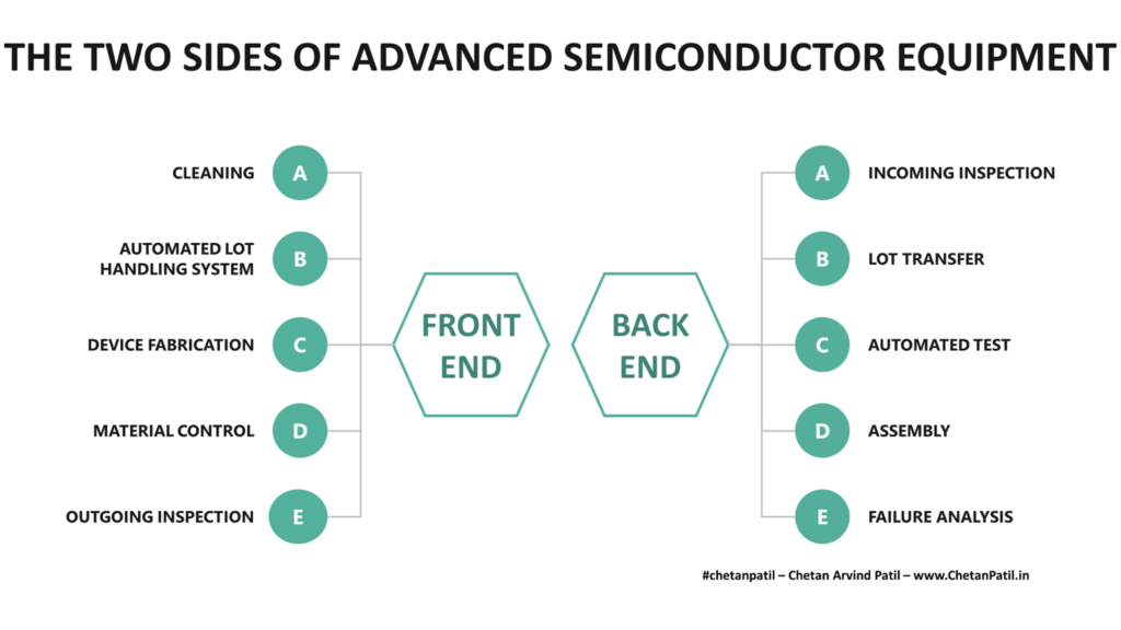
    End-To-End Process: Semiconductor industry is built on top of several segments, which includes the design houses to equipment manufacturers to FABs to manufacturing OSAT sites, and many more. All these individual segments should be connected end-to-end to provides a holistic view of how the product development, manufacturing, and delivery flow. This is where cloud-based solutions are useful, and such solutions also bring transparency.

    To create a robust and high-quality semiconductor product, numerous data points are required. This is possible only with the help of tools and solutions that connect and provide a detailed view of different stages of the product development cycle. This is why a cloud-based end-to-end solution is heavily used in the semiconductor industry.

    As more FABs and OSATs get established in different parts of the world, the cloud strategy should be one of the top priorities. Doing so, will only increase productivity and enable a better customer experience.


    Picture By Chetan Arvind Patil

    Picture By Chetan Arvind Patil

    THE USE OF CLOUD IN SEMICONDUCTOR INDUSTRY

    Cloud-based solutions are used at every step of semiconductor product development. The efficiency and productivity such tools bring to different stages of product development, ensures that the end-product is defect-free.

    Different segments of the semiconductor product development require a unique cloud strategy. These can range from specific EDA tools to massive data storage instances. In the end, all these data points are connected/tied to a specific product. This way any team from anywhere can access the needed data/information to execute the task at hand.

    Research And Development: Designing devices to form the circuits and layouts that will eventually get fabricated into a silicon product, is the first step towards developing a turnkey semiconductor solution. For several years, the semiconductor industry has relied on software-based solutions. In the last decade, the same software has moved from desktop to cloud. This has enabled designers and researchers to access files and libraries on-the-go. On top of that, it has taken away the need to have high-performance systems that were earlier required to carry out tons of simulations. Today, one can simply deploy and get on with other work while the simulations are running on the cloud. Using the cloud, companies can ensure that there is no IP infringement as the check can run on the fly and tools can compare design solutions against the massive poll of cell libraries. All this ensures that the right product is developed by following the industry-standard protocols.

    Data Analysis: Data generation occurs at every stage of silicon development. Whether it is simulations in our design stage or fabrication/testing in FABs/OSATs. This is why advanced statistical analysis is carried out on every data point that is generated. Doing so on the fly means deploying solutions that can run closer to the data generating source. Also, if the data source is error-free, then data engineers can question it and take a deeper look by using analytical tools. In both scenarios, highly advanced tools are required. This means making use of cloud-based solutions that are easy to access and are loaded with features to enable accurate data exploration.

    Supply Chain Management: Delivering products to the end customer often requires connecting several dots from different systems. This is why supply chain management is needed. It ensures the product and its processes are tracked using the unique bill of materials. This often requires relying on specific cloud-based tools that can swiftly retrieve any information related to the products to provide its full history from inception to delivery. Such a task without cloud tools will certainly invite errors.

    Market Analysis: Capturing market trends to understand which products will give maximum profits is key to success. This often requires capturing different data points and then aligning the product roadmap as per the market (which means the customer) requirement. This ensures that the CapEx is diverted towards high revenue products. Such planning and projection are not possible without capturing different data points and customer developments. This is where cloud-based market analysis comes in handy and ensures that the projects are profitable.

    Resource Management: Semiconductor equipment, tools, and labs require high CapEx and such investment is viable only if there is a high ROI. To achieve positive ROI, the resources need to be looked after and that requires efficient management. This means periodic maintenance to ensure minimum downtime. For such management, cloud-based solutions are deployed so that whenever tools go down or require maintenance, the data can be captured to raise the alert beforehand.

    Factory Operation: Running FABs and OSATs 24×7 is key to ensuring that the facilities breakeven as quickly as possible. This requires capturing second to second activity of every corner of the factory. This is possible only when a connected system is deployed that can raise alarm in case of downtime and also provide remote status of every piece of equipment and tools. Cloud-based solutions already play a key role in this can thus are heavily used by semiconductor FABs and OSATs.

    Logistics: Shipping is a big part of the semiconductor product development cycle. The wafers often come from a different outside supplier and then get fabricated at a different location, only to get tested in a different part of the world. This means optimized logistics and real-time tracking of material. While the majority of the logistics solution providers are heavily using cloud-based solutions to track and deliver packages, it so often happens that the semiconductor companies also have to invest internally in systems that can raise shipping labels apart from tracking where the customer deliveries are. This is why cloud-based logistics solutions are handy for semiconductor companies.

    Archiving: Saving every data point related to the product is vital. This data ranges from design files to test data to financial records. All these need to be stored for a very long term so that whenever a query or comparison has to be done, the data can be easily retrieved. Quick retrieval and analysis are only possible if cloud solutions are deployed.

    The use of the cloud in the semiconductor industry will keep growing. In the next few years, more sophisticated and smart tools will be deployed. Factory operations are already utilizing high-tech cloud solutions for product fabrication. Design and Supply Chain Management are not behind. The cloud market for the semiconductor industry will only keep growing with more new players entering the product development every year.


  • The Pillars Of Semiconductor Industry

    The Pillars Of Semiconductor Industry

    Photo by Tanner Boriack on Unsplash


    THE IMPORTANCE OF PILLARS IN THE SEMICONDUCTOR INDUSTRY

    There are numerous industries worldwide catering to different markets. Company from a specific industry will rarely provide all end-to-end in-house solutions to develop products.

    Almost all of the companies within a given industry rely heavily on different segments (from the same industry) to achieve the goal of producing high-quality products for their target customers.

    The same fundamentals are valid for the semiconductor industry. Without the support environment, the product will not meet the high-quality customer’s expectations. More so, when the silicon chip can be used for numerous types of applications anywhere in the world. That is why quality and reliability need to be above par.

    To satisfy customer requirements, different types of support systems are needed. In semiconductors, these support systems can be called pillars. These pillars of the semiconductor industry can be logically separated into three different segments

    Front-End: Research, design, and marketing.

    Middle-End: Support, equipment, and software.

    Back-End: Manufacturing, supply chain, and sales.

    Each of these three segments plays a crucial role in bringing a product to the market. They do so to provide the following important traits:

    Cost: Semiconductor companies are immensely focused on cost reduction to grow their product margin. This is something that requires three-way synchronization of the three discussed segments. These segments to do by bridging together the gaps that ensure zero-delay and zero-waste. Such practice ends up creating low-cost but high-quality flow for the semiconductor product development.

    Time: Delivering products on time is the key. Delays in projects can hurt a company’s reputation and growth. This requires all three segments to work in harmony. Using the data-sharing approach, different segments work together to ensure all possible delays are eliminated, thus ensuring time-bound delivery.

    Growth: Connecting the three segments seamlessly, ensures that the product is profitable in the long run. Ensuring there are no gaps between the three segments enables a high growth margin too.

    Quality: Working with different segments within the same industry also requires efforts to maintain high-quality and standards. This is what these three different segments work towards by ensuring different tools and processes come together to provide reliable products.

    Innovation: In the end, companies in semiconductors are focused on innovating next-gen solutions. This is possible only when all three segments are set up and connected to drive innovation, which often requires a high level of operational management, something Front/Middle/Back segments have incorporated for a long time.

    The three different pillars of the semiconductor industry play an important role when it comes to product success and profitability. However, it takes a lot of effort and time in building a network of solution providers that form a robust three-way network.


    Picture By Chetan Arvind Patil

    Picture By Chetan Arvind Patil

    THE ROLE OF DIFFERENT PILLARS IN THE SEMICONDUCTOR INDUSTRY

    The semiconductor industry views Front-End, Middle-End, and Back-End from a technology-node or semiconductor fabrication point of view. However, it is about time that the world also sees these three segments from a business point of view.

    Each of these three segments is vital in ensuring that the product is delivered to the market on time.

    Front-End: Front-End segment captures customer/market requirements which are used by teams to design a product. This is the research and development part that brings product ideas to reality. It can also be seen from a marketing point of view as a stepping stone towards next-gen products.

    Middle-End: Middle-End segment connects the design and marketing side of the product to the back-end side that delivers the fabricated product to the end-customer. It also consists of different support environments like software, equipment, facilities, and so on.

    Back-End: In this segment, the product comes to life. It is more manufacturing, logistics, and the supply chain side that ensures the design reaches the market in time. Back-End is also about working with different assembly teams to ensure the semiconductor product is mounted on the system works as per the specification.

    It might be confusing to the industry veterans who have only focused on Front/Middle/Back end systems from a fabrication point of view, but as the world is moving towards more connected product development it is equally important to understand how and which segments within the industry work in synchronization to enable advanced technology.

    Viewing the end-to-end semiconductor industry chain from the above three pillars gives a more realistic view of how the semiconductor industry works and the importance each of these segments/pillars brings.


  • The Role Of Root Cause Analysis In Semiconductor Manufacturing

    Photo by Mathew Schwartz on Unsplash


    THE IMPACT OF SEMICONDUCTOR ROOT CAUSE ANALYSIS

    Delivering high-grade products is the ultimate goal of every manufacturer. To do so, different industry-specific standards and processes are used. The same applies to the semiconductor manufacturing industry.

    In semiconductors, as the technology-node shrinks, the cost to manufacture tiny silicon increases too. To ensure there is no waste of materials, time, and cost, several different strategies are deployed to screen the part before it moves ahead in the fabrication/manufacturing line.

    One such strategy is root cause analysis. It so often happens, that the product being developed might encounter an issue during the qualification, testing, or packaging stage. Does not matter where the failure occurs, it is critical to understand the root cause. For an industry like semiconductor manufacturing, where every failing part can jeopardize not only the product quality itself but also the system to which it will eventually get glued in to. Such a scenario can certainly lead to millions of dollars in losses apart from a negative business reputation.

    This is why holding on to every failing product and carrying out detailed root cause analysis is one of the major pillars of the semiconductor industry.

    Over the last few decades, as the devices are getting tinier than ever, the importance of root cause analysis is growing due to the several impacts it has on the product:

    Cost: Finding the root cause of why the product failed, empowers the team with data points to take necessary actions. It so often happens that the root cause analysis is more about setup or lab where the qualification or testing is being carried out and has nothing to do with the product itself. All root cause analysis and actions eventually can save cost by eliminating the need to re-do either the design or the qualification. Root cause analysis of failing products also ensures that the product will not fail in the field, thus saving years of investment.

    TTM: Given the stiff competition in the semiconductor industry, the ultimate goal of every design and manufacturing house is to ensure that the product is launched within the planned time frame. In case of failures, root cause analysis provides a way to capture any severe design or process issue early on. This allows course correction to ensure the product still makes it to the market in time.

    Quality: Qualification is an important process before the product gets released for production. Root cause analysis of any failing product during the development stage ensures that the product meets the high-quality industry standards. The standards increase as per the target domain and so does the importance of root cause analysis of the failing product/part.

    DPPM/DPPB: Defective Parts Per Million/Billion is an industry-standard metric. The goal of semiconductor manufacturing is to lower DPPM/DPPB. In case of field failures, root cause analysis comes in handy, as it ensures the severe fails are captured to lower the DPPM/DPPB further. More so, when the product/part will be used for critical applications like automotive or wireless communications.

    Root cause analysis has a major impact on semiconductor manufacturing. With new FETs and equipment launching every year, the role played by analyzing any smaller to big product-related failure is vital for both FAB and FAB-LESS companies.


    Picture By Chetan Arvind Patil

    THE STEPS OF SEMICONDUCTOR ROOT CAUSE ANALYSIS

    To capture the root cause that leads to the failure of a product, several steps are followed. Each of these steps plays a key role in providing data points to establish the root cause to drive defect-free manufacturing.

    Inspection: Any given part/product that fails first and foremost has to go through a detailed inspection. Depending on the state of the product (whether in wafer or die or assembled packaged form), the inspection is performed. The images generated by these are then used to establish if any non-technical cause (handling, stress, recipe issue, etc.) leads to the failure of the product. X-Ray and SEM are widely used as these processes provide internal product details.

    Data: The data points for the failing part/product come from different stages. All the parts have marking to trace their origin. As a starting point, the first data point is collected by testing the product without damaging it. Another data point can be inspection data that FAB and OSAT might have on the failing part/product. Apart from these two, several other data points like recipe error, handling issue, the material used and many more, are captured to establish whether the root cause can be determined based on the data itself.

    Testing: Testing can be done performed on: ATE and BENCH. On ATE, the part/product is tested to capture failing tests. This provides an early hint about which blocks of the part/product are failing. In case, there is no firm conclusion, then BENCH validation allows a way to find if the part indeed failed or there was a setup error. In many cases, different testing scenarios are also used to capture testing-related data points.

    Reproduce Failure: This is the basis of the root cause analysis. Once the failure mode is understood, then the setup is replicated with an exact error to understand if the part/product repeatedly fails or not. This often requires a good setup and good parts/product, with the only varying parameter being the setup to capture the failing scenario/setup.

    Localization: Root cause analysis can also lead to the discovery of issues in the product itself. This often requires the team to perform the root cause analysis to establish the location at which there are design issues. This is achieved with the help of all the above steps and most importantly using the equipment to show that when the part/product is biased, then it fails due to a hotspot found on the specific location of the layout. Advanced equipment are used to capture such data.

    Documentation: In the end, everything needs to be documented. Documentation is a major part of not only capturing the reasons for part/product failure but also enables cross-functional learning. In the future, the documentation can be used to minimize the efforts to establish root cause in cases where the failing trend is similar. 8D and other problem-solving methods are used to document detailed root cause analysis.

    Finding the cause of failure is like finding a needle in the haystack. The complexity the products are bringing, (due to advanced technology-node) is making root cause analysis an important and also difficult task at the same time.


    Picture By Chetan Arvind Patil

    THE PILLARS OF SEMICONDUCTOR ROOT CAUSE ANALYSIS

    Performing root cause analysis is certainly a team effort. Experienced people play a vital role in reducing the time it takes to establish the root cause.

    However, there are two major pillars without which root cause analysis is not possible. These pillars also require massive investment to establish and often have a high operating cost.

    Lab: A dedicated space is required where experienced engineers can take the failing part and establish the root cause by biasing the part in a controlled environment. This requires skill-based training and the ability to understand any failing product/part that comes into the lab.

    Equipment: To run a root cause analysis lab, advanced equipment are also needed. These equipment can perform detailed inspection, apart from carrying out different setups/testing to reproduce the failure.

    The majority of the semiconductor companies have an in-house dedicated lab to perform root cause analysis. Some companies prefer to outsource. Eventually, it is all about managing resources and lowering the cost without compromising on the DPPM/DPPB.

    As the industry moves towards more complex products that will power everything everywhere, capturing the root cause of every failing product during development or the production stage, will become more vital than ever.


  • The Ever Changing Semiconductor FET

    The Ever Changing Semiconductor FET

    Photo by Carlos Irineu da Costa on Unsplash


    THE IMPORTANCE OF SEMICONDUCTOR FET

    Cells are the building blocks of life. Similarly, transistors are the building blocks of the semiconductor industry. In the computing world, transistors lay the foundation for any type of processing solution.

    Transistor performs the basic function of toggling between HIGH (ONE/TRUE) and LOW (ZERO/FALSE) state. Such basic function when performed by zillions of transistors together, drives several technological solutions from car safety to wireless data/voice transmission.

    The need to make compact computer-powered solutions has pushed the development around the transistors over the last four decades. These development have been both on the design and the manufacturing side.

    Transistors used in semiconductors are often called FET – Field-Effect Transistors. The function performed by FETs is the same as traditional transistor. The only aspect that has changed over the years is the form factor which changed in order to follow the Moore’s law.

    The main goal of FET is to improve Power-Performance-Per-Area (PPA). To do so, following technical aspect has to be fulfilled before the FET design can be used to manufacture next-gen hardware:

    Operating Voltage: A perfect FET will be the one that can perform as per the specifications. As the technology-node shrinks, the operating voltage also goes lower due to the advancement in the FET design. The major reason is to accommodate the dynamic and static power consumption along with the leakage. Lowering voltage has negative impact to, but that is compensated with the unique designs of next-gen FET.

    Process Technology-Node: Technology-Node shrinks faster than the development of new devices. Till then the devices go through a different non-planar to planar transformations to accommodate for the shrinking size. However, after a given point it becomes design and manufacturing-wise difficult to transform (like FinFET can only be stretched to a certain extent with the help of its fins) the same device type. After that, the material and drastic design changes are expected.

    Power Consumption: FETs are present in a large number in any advanced technology-node systems like microprocessors. If FETs are not providing the lower dynamic power consumption (along with negligible leakage), then the purpose to use new designs is not fulfilled. Hence, device designers face an uphill challenge to ensure the increased density of the FET in a specific silicon area only leads to lower power consumption, not higher.

    Performance Improvement: Apart from lower power consumption, performance improvement is another criterion that leads to new FET designs. Balancing power consumption along with performance is difficult. However, without these criteria, there is no way to ensure the next technology-node will have a better impact and use case than the previous one.

    Impact On Area: Eventually, the goal of shrinking technology-node is to ensure the area of the silicon chip does not increase for the same or more computing tasks. This means the design of new FETs will have to be more 3D than 2D/2.5D. Otherwise, in the long run, it becomes a bottleneck for the designers to make use of the FET without impacting the silicon area.

    The FET is the building block of modern semiconductor solutions and there are already several types of FET that are available and used based on the technology-node.

    Both academia and the industry have contributed equally in bringing new FET design to the market, which today is powering almost all of the electronic products around the globe.


    Picture By Chetan Arvind Patil

    THE RACE FOR NEXT-GEN SEMICONDUCTOR FET

    Given the race to be the first one to launch the next technology-node, the semiconductor companies (mainly semiconductor manufacturers) are also racing to come up with a new FET design that can cater to their needs while having minimal to zero impact on Power-Performance-Per-Area (PPA). During this course, the semiconductor industry has already seen many transformations in FET designs. From 2D to 3D.

    Below are few active and future FET designs that the semiconductor manufacturer is pursuing:

    Planar FET: These are the traditional FET that follow the 2D design. The source, the drain is on top of the substrate and is not wrapped around the gate. The power consumption and area impact is high. Planar FET mostly use nanowires.

    FinFET: FinFET is an advanced version of planar FET. The source and drain are extended as fins and the gate wraps around them to provide a faster current flow. One drawback of FinFET is that the design might lead to manufacturing residuals around the fins. This can impact the quality of silicon chip being manufactured. However, FABs have found ways to ensure there are enough inspection steps to avoid such defects. FinFET is what today the majority of the manufacturing companies use to manufacture silicon requiring advanced technology-node.

    GAAFET: FinFET has its advantage, however, to provide lower operating voltage and higher performance, the industry has also come up with GAAFET. GAAFET is geared to be used towards 3nm mass production along with FinFET. The difference between GAAFET and FinFET is the slicing of fins by making of nanosheets to drive much faster current flow that FinFET. This also allows greater switching control. This structure helps in shirking the size without impact the performance.

    MBCFET: MBCFET has been developed by Samsung as part of their 2nm and beyond technology-node roadmap. Both FinFET and GAAFET use fins that are stacked vertically, thus not allowing the use of the area above the source and drain. To overcome this, MBCFET is developed that uses the same fins based nanosheets but are stacked horizontally to provide more area for current flow. MBCFET can also be designed using existing process tools and has the same area footprint as FinFET and GAAFET.

    CFET: While the industry moved towards fin-based structure and started using nanosheets to provide more area within the same size, researchers have also been focusing on CFET which they are touting to be the next-big thing in FET design. The CFET is an advanced version of fin-based FET (even more advanced than MBCFET) and it uses the folding approach to keep nFET on top of the pFET. This can be done either via fins or sheets. It is like a high-rise structure with FETs stacked on top of each other. CFET still uses a nanosheet approach.

    NGFET: These do not exist today. NGFET – Next-Gen FET – will be what the semiconductor industry will use when going beyond 1nm. It will borrow all the learnings from the prior generation, however, instead of nanosheet, NGFET will use forksheets. The forksheets will take a nanosheet approach by combining the vertical and horizontal fins to provide more density and performance.

    While there are several FET solutions to choose from, the industry and the academia do understand the difficulties the semiconductor design and manufacturing bring when advanced technology-node process is used. Thus, leading to several new (and known) hurdles and challenges.


    Picture By Chetan Arvind Patil

    THE HURDLES FOR FUTURE SEMICONDUCTOR FET

    Given the small area for improvement, new FETs are incredibly complex to design. While both the academia and the industry is focused on improving the FET design that lowers the operating voltage while balancing other technical specifications, there are certainly numerous hurdles to overcome.

    Voltage: The smaller/advanced the technology-node, the lower the operating voltage. The primary reason is the ability to generate heat or damaging the devices (= FETs) when operated at a higher voltage. With every new generation/type of FET, the operating voltage is low. This also impacts the sub-sequent systems the advanced technology-node systems (using lower operating voltage FETs) are connected to. This means a new system is required to drive the data further at higher voltages. As FETs evolve beyond 3nm technology-node, such design constraint is something the device designers will have to consider so that the operating voltage is not too low for the silicon system down the line.

    Leakage: Lowering technology-node means new device structures and it also means more transistors per given area. Operating all these devices at higher voltage can subsequently lead to leakage either through continuous operation or via thermal. Lowering the leakage is another challenge for FET device designers.

    Thermal: Thermal is a tricky one to solve. The junction temperature is already high enough that it demands designers to embed temperature sensors to capture thermal effects. This certainly adds complexity to the design and also impacts the operating scenarios, which hinders from exploiting the full potential of the systems due to continuous throttling.

    Performance: Lowering operating voltage as the FET evolves means also balancing the performance and area ratio. FET in the future will have tackle this three-way balancing act (voltage, performance, area) as the industry marches towards the 2nm and lower technology-node.

    There are certainly several hurdles (apart from those listed above) for FET design and manufacturing. The semiconductor design and manufacturing industry will overcome these and many. Academia is also coming up with interesting FET solutions that can pave way for more elegant lower technology-node solutions without compromising on the voltage to performance to silicon area.

    In the end, the FET design will keep changing and evolving in order to keep pushing the semiconductor industry forward towards More-Than-Moore world.


  • The Contest For Next-Gen Semiconductor Package Technology

    The Contest For Next-Gen Semiconductor Package Technology

    Photo by Ryan on Unsplash


    THE MOVE TOWARDS THE NEXT-GEN SEMICONDUCTOR PACKAGE TECHNOLOGY

    Packaging plays an important role in almost all the industry. From cars to rovers, packaging the product before shipping is vital. Doing so cost-effectively is critical to ensure the product cost is not affected.

    The same story is valid for the semiconductor industry, where the packaging technology ensures that the silicon die is protected from harsh mechanical to environmental conditions.

    In a nutshell, package technology in the semiconductor industry is geared towards providing the following features to the die area:

    Thermal: Ensure the heat is dissipated efficiently out of the die to avoid thermal runaway.

    Mechanical: To save silicon from any outside impact like vibration or stress.

    Connectivity: Enable a pathway for connecting the die to another system via a printed circuit board.

    Contamination: Protect the die are from contamination due to long-term usage.

    Today, there are numerous package technologies to choose from. Eventually, the decision to decide on the package type is based on both the technical and the business points.

    Give the advancement in the semiconductor design and ever-shrinking technology-node, it is becoming a challenge for semiconductor packaging solution providers to come up with innovative packaging solutions that are also low-cost. All this is pushing the need for next-gen – InFO, CoWoS, CoC, FCiP, PoP, and many more – package technology solutions.

    The push towards next-gen package technology is driven by several factors:

    Die: Semiconductor product development is moving towards More-Then-Moore solutions. This means several new die-based solutions and one of them is chiplets. Chiplets is IP driven design process, where different die come together to form the same system which earlier would have been a single die. Chiplets are proving to be effective both from a cost and yield perspective. To cater to such requirements, package technology solution providers (OSATs) have to keep their innovation team engaged, to ensure not only the packaging solution is at-par with chiplets requirement but are also low-cost due to the stiff competition.

    Design: One example of modern semiconductor design change is the heterogeneous architecture. It has provided ways to bring different types of XPU together. This also requires an efficient way to package by considering the thermal profiles of such complex and high-frequency devices.

    Size: The shrinking size is also adding to the need to be more innovative in package technology. Not all devices will be small and at the same time also not too big. OSAT is facing a challenge to cater to different markets and while doing so, have to ensure the type or size of the device is not a constraint.

    Workload: Emerging workloads are becoming complex year-on-year. These workloads running on the die continuously end up heating the system. To mitigate such issues, new materials and packaging solutions are required. This is also one reason that is pushing OSATs towards next-gen package technology.

    OSATs have to continuously provide solutions that cater to both the smaller and larger die areas. This has to be done in coordination with the design houses, to ensure that next-gen package technology meets all customer requirements.

    However, lately, OSATs are being pushed from all the corners and are getting beaten in their own game by FAB-LESS to FAB houses.


    Picture By Chetan Arvind Patil

    Picture By Chetan Arvind Patil

    THE RACE TOWARDS NEXT-GEN SEMICONDUCTOR PACKAGE TECHNOLOGY

    The semiconductor package technology is mostly enabled by the OSATs. IDMs also play a crucial role. However, given the rise of the semiconductor packaging and testing business, OSATs are facing stiff competition from FAB and FAB-LESS companies too.

    This is leading to both positive and negative impact on all types of semiconductor companies:

    OSAT: The primary focus and strength of the OSATs have been the testing and packaging solutions. With growing competition from FAB on the packaging solutions is certainly putting OSAT in a position to not only innovate on the testing to packaging arena but also how to expand the business beyond traditional OSAT services. This certainly diverts the focus of OSATs, as it is more difficult to move towards FAB or FAB-LESS business while also catering to the same customer type.

    FAB: FABs all over the world have the biggest advantage due to the availability of high-tech and research facilities that can aid the innovation of next-gen package technology. This is why TSMC and Samsung have been at the forefront of next-gen packaging solutions. At the same time, FABs are also diversifying and entering the OSAT business with a strong packaging portfolio. 

    IDM: IDM has always enjoyed the best of both world. Intel already has many homegrown packaging solutions for its need, apart from the ability to fabricate, test and assembly in-house. The innovation in the design space is only benefitting IDMs as they can foresee and quickly adapt their business by pushing towards the required semiconductor packaging research and development activity, and quickly turn research into production-worthy solutions.

    FAB-LESS: While, majority of the FAB-LESS companies only focus on the design side. The need to have a packaging solution that can cater to their designs is also pushing FAB-LESS to continuously invest time and money in the packaging technology.

    Eventually, packaging solution for semiconductor products is driven by cost optimization. The innovative and low-cost packaging solution catering to the next-gen design will win the race. However, to do so massive research and development activity is required. Which certainly demands high CapEx.

    To balance the complexity and high CapEx, packaging solution providers (OSATs mainly) will have to be more innovative to ensure the next-gen solution is business-friendly.

    The race towards next-gen semiconductor package technology is certainly heating up, however, it is also an opportunity to innovate and create a new market for the emerging solutions.


  • The Roadmap For In-Country End-To-End Semiconductor Industry Growth

    The Roadmap For In-Country End-To-End Semiconductor Industry Growth

    Photo by Laura Ockel on Unsplash


    THE REASON WHY COUNTRIES ARE PUSHING IN-COUNTRY SEMICONDUCTOR GROWTH

    The basic and the applied science form the base for any technological advancement. Countries globally have always focused on the importance of these two aspects of science. That is why countries race against each other and invest a lot of time and money to lead science that enables technology.

    In the 21st century, the focus on applied science (basic science is not behind, maybe ahead in several aspects) skyrocketed due to the proliferation of digital devices and wireless connectivity. Only a handful of countries quickly realized the importance of leading in a technological solutions that forms that base of a modern digital solution. Some focused heavily on the research and development (design) of novel technologies (WiFi to 5G to autonomous to robotics and beyond), while others emphasized the need to manufacture these for the end customers.

    Semiconductors Are Everywhere

    The semiconductor industry also can be seen by separating out into design and manufacturing. Countries like the USA focused more on the design aspect of the semiconductor, while Taiwan and China ramped up manufacturing efforts. This worked well until the 5G and COVID raised concerns over the growing inter-dependency, and then started the saga of how leadership in the semiconductor design and manufacturing affects day-to-day technological (from satellites to cars) solutions. This in turn started pushing several other countries (India to Australia and beyond) to focus on the need to design and manufacture semiconductors in-country.

    There are several reasons as to why countries (which are behind) should focus on end-to-end in-country semiconductor industry (or at least have enough infrastructure to cater to in-country demand):

    Dependency: Relying on other regions for manufacturing or designing semiconductor products is one reason that is pushing countries to focus on the in-country end-to-end semiconductor solutions. This also includes materials to equipment. It is difficult to make everything in-house, hence good enough infrastructure to cater to the local consumer demand and critical national infrastructure of the county is a good way to start.

    Import-Export: From smartphones to cars, all are heavily powered by semiconductor solutions. In trade, it is good to keep imports and exports in balance. Countries without vital semiconductor (manufacturing) infrastructure will always end up importing more than exporting. This will put pressure on their forex reserves and will make them fully dependent.

    Growth: The semiconductor market is growing due to the growth of semiconductor usage in the modern infrastructure/technology. Automotive is one example, apart from the consumer market, and many other industries where semiconductor solutions are used by default. Countries should capture a portion of the market which will eventually generate employment and business growth. This is critical for long-term financial stability too.

    Business: Establishing a high-tech industry like semiconductors (mainly manufacturing, as many countries do have design houses) will not only lead to market growth and employment but will also support other businesses that eventually are the pillars for the semiconductor industry. It can be from equipment manufacturing to raw materials to turn-key (and ever-expanding) civil engineering work to build FABs/OSATs.

    Above points fueled with the growing use of semiconductor in all the major infrastructures and technological solutions (that affects every aspect of day-to-day life) is more than enough reasons for countries with lacking semiconductor manufacturing infrastructure to start today for tomorrow’s need.


    Picture By Chetan Arvind Patil

    THE ROADMAP FOR IN-COUNTRY SEMICONDUCTOR INDUSTRY SUCCESS

    There are 195 countries and each one of these have their own strengths and weaknesses. It is difficult to create an end-to-end in-house solutions for the semiconductor industry. More so, when the goal is to drive in-country semiconductor growth to the next level.

    In reality, there are no roadmaps that countries can follow to gain momentum for an in-country semiconductor to make themselves self-reliant. On other hand, countries today also cannot overlook the importance of having as many points checked from the roadmap that can enable, if not end-to-end, some parts of the semiconductor supply chain. This will allow them to tap into the future market needs and ensure stability in semiconductor market.

    The roadmap to success in the semiconductor industry consists of many points and below are the few major ones:

    Talent: Nothing can be developed without having the right set of talent (human resources). Countries already have a framework to educate their population. However, the traditional education system is still focusing on core aspects that enable basic training. While there is no harm in doing so, it is about time that countries wanting to engage in in-country semiconductor growth (manufacturing and beyond), needs to start with training programs that focus more on core semiconductor on-field training programs apart from the fundamentals.

    Policy: Eventually, investment is a big part of semiconductor growth. While countries looking to steer ahead in the in-country semiconductor solutions have already started to come up with incentives and policies, the approach should be more holistic that focuses not only on the semiconductor growth but also on the regional infrastructure required for the semiconductors. This may be from ensuring airports to logistics to man-power availability, apart from ease of the land and housing facilities.

    Infrastructure: The semiconductor supply chain is heavily driven by the turn-key infrastructure. From FAB-LESS to FABs to OSATs, all require support infrastructure to ensure the products reach the market in time. This infrastructure varies from material handling to chemicals transportation to water availability to non-stop electricity. Building FAB/OSAT is one thing and running it non-stop is another. The better the support infrastructure for the semiconductor industry, the more likelihood of semiconductor giants willing to setup future-focused manufacturing setups.

    Public-Private: Government support plays a very key role in driving in-country semiconductor growth. This can be from investing in the required infrastructure to providing incentives that can ensure required investment is available to drive manufacturing facilities. A two-way shake hand between the private players and public bodies can drive the needed policies that are friendly to both the businesses and the consumers.

    Research: Research is key to long-term semiconductor growth. Countries focusing on the in-country semiconductor ecosystem should provide research funding (mainly countries with lack research funding support) to universities and colleges to focus on the next-gen semiconductor devices and manufacturing solutions. Universities and colleges themselves also can raise funding via industry collaboration with the semiconductor companies.

    Academia: Education is vital to every aspect of industrialization. The majority of the countries already have the infrastructure to educate the future workforce. However, the goal to make semiconductor in-country growth requires academic institutes to focus on semiconductor engineering courses apart from the traditional engineering domains.

    Cluster: FAB requires billions of dollars before it can run at full capacity and then it takes years to break even. Even then, due to changing technology-node and solutions around it, the process to upgrade FAB is a continuous one. Countries without a FAB wanting to attract/setup one, should focus more on the cluster approach. Cluster-based FAB can be a pooled investment for higher technology-node (older but relevant) that caters to different semiconductor FAB-LESS companies. Such kickstart can then lay the foundation of dedicated sub-10nm foundries.

    Outreach: Outreach is about reaching out to other countries and also attracting businesses to showcase what a specific country can offer. This way there is a dialog between the public and private players that can lead to many business opportunities in the semiconductor sector. Countries should do outreach by default, if the goal is to setup the semiconductor manufacturing (FABs to OSATs) in-country.

    Future-Tech: Countries that have semiconductor design houses but not manufacturing facilities should set the target on what the world will need in 2040 and not in 2030. This can range from chiplets manufacturing (semiconductor specific) to next-gen 6G wireless solutions to flexible electronics. Doing so will ensure that the companies and countries are creating infrastructure today for tomorrow’s demand. This can give an edge over countries with massive semiconductor manufacturing infrastructure and are not willing to invest further without closing/upgrading existing semiconductor infrastructure.

    The above roadmap points cover the majority of the aspect of ensuring in-country success in the semiconductor industry. There can be different points that also are vital for the semiconductor industry growth. In the end, it all boils down to what eventually works and what does not.


    Picture By Chetan Arvind Patil

    THE LONG TERM IMPACT OF IN-COUNTRY SEMICONDUCTOR INDUSTRY

    The last two years have shown the growing importance and emphasis on the need for in-country semiconductor industry growth. Countries are putting efforts to lead in every aspect of the semiconductor solutions, mainly in order to make themselves less reliant on other countries while also taking lead in the advanced modern technological solutions.

    The in-country semiconductor growth will have two major long term impact:

    Self-Reliance: Countries that can take the lead in the semiconductor industry growth will make themselves self-reliant in the long term. Which will prove vital in the long term due to the fact that the consumers solutions to national infrastructure is fully reliant on the semiconductor powered solutions.

    Leadership: There is no denying that every country is racing to claim leadership in every aspect of the modern world. Leadership in the semiconductor industry is certainly going to veto on who gets to call itself the superpower.

    It is good that the semiconductor industry is getting the focus, but countries will have to be diligent in understanding what works and what does not works as per the demand and supply requirements.

    In the end, investment to get semiconductor manufacturing up and running is huge. Any miss-step will put countries behind instead of going ahead. It also takes years of planning to create any kind of massive (and advanced) infrastructure.

    Hopefully, the global supply chain the semiconductor industry runs on, stays intact even with in-country semiconductor infrastructure race.


  • The Impact Of Advanced Equipment On End-To-End Semiconductor Process

    The Impact Of Advanced Equipment On End-To-End Semiconductor Process

    Photo by L N on Unsplash


    THE NEED OF ADVANCED SEMICONDUCTOR EQUIPMENT

    High-Tech manufacturing is not possible without the use of equipment. The equipment ensures that the product being manufactured is defect-free and also meets the quality requirement for the target market.

    The same fundamentals apply to the semiconductor industry, where equipment plays an important role. Given the need to fabricate semiconductor products without even touching the wafer/die area, requires equipment that can do the task and that too without adding delay or defects.

    Every stage of the semiconductor product development requires high-tech equipment, that is why semiconductor fabrication, testing, and assembly facility is 90% occupied by the equipment. These advanced equipment require only a set of commands (called recipes) to complete the task they are assigned. The automation achieved with this process ensures the FAB/OSAT are running at full capacity 24x7x365. This is why it is often a challenge for the semiconductor FAB and OSAT to ensure the equipment never goes down and this requires periodic maintenance that is often driven by data collection and analysis.

    Semiconductor FAB and OSAT often have two different types of equipment:

    Advanced: Advanced equipment is often robotic driven. This includes moving the wafers and other materials (mainly reticle). Apart from robotic capabilities, advanced equipment often has data capturing capability that is then stored for further wafer/die analysis.

    Non-Advanced: These types of equipment in the semiconductor process are confined to analysis or lot transferring, and do not have the robotic capability and are more useful for manual inspection or testing.

    Majority of the equipment in the semiconductor FAB/OSAT are advanced and are designed for the following goals:

    Yield: Primary target of any semiconductor FAB/OSAT to ensure there is minimal to zero yield loss. This is only possible if the process of handling and using materials (reticle, wafer, etc.) adheres to the standards that ensure high-yield. This is where equipment come into the pictures, and the materials are handled and processed in a manner that does not negatively affect the semiconductor wafer, thus ensuring minimal yield loss.

    Quality: Quality is the primary de-facto target of every semiconductor product. Equipment can be handy to capture any issues/variations/excursion during the semiconductor process. Whether it is during the lithography stage or automated inspection, equipment ensures the process being executed is eventually leading to correct wafer/die formation.

    Capacity: The primary target of FAB/OSAT is to ensure the facility is 100% utilized. This is only possible if there is an advanced equipment that is working non-stop day in and day out. Without investing in the equipment to increase efficiency, it is not possible to utilize FAB/OSAT fully.

    Accuracy: Advanced equipment is also important from an accuracy point of view. They ensure the target design is fabricated without any gaps. From etching to deposition to even assembly, accuracy/alignment can only be achieved if the equipment is used. If the manual process is used, then it will not only lead to errors but also bring the FAB/OSAT capacity down.

    Throughput: Semiconductor products get utilized by different industries and markets. To timely provide them with the products requires high efficiency. This is made possible by advanced equipment that can process wafers after wafers to keep up with the demand. On top of this, any given FAB has numerous parallel equipment doing the batch processing, thus ensuring the throughput is always at the maximum level possible.

    The semiconductor FAB/OSAT are utilizing advanced equipment to keep the facility running that eventually drives revenue. However, ever changing technology-node and device structure is also putting pressure on the FAB/OSAT to upgrade their equipment often.

    While the majority of the advanced equipment has a plug-and-play feature for easy upgrades, CapEx and maintenance teams are required to keep the equipment running which in turn runs the FAB/OSAT.

    Irrespective of the features or the CapEx hurdles, advanced semiconductor equipment is vital for high-quality semiconductor product development.


    Picture By Chetan Arvind Patil

    THE TWO SIDES OF ADVANCED SEMICONDUCTOR EQUIPMENT

    There are different types of advanced semiconductor equipment that are used by the FAB/OSAT. They often get categorized based on which part of the wafer fabrication the equipment is used for.

    Front-End: The advanced equipment for the Front-End process is used in a semiconductor FAB. There are different advanced equipment that does the task as per the process flow they are part of.

    Cleaning: This process utilizes equipment to clean wafers/lots post a wafer stage. Whether cleaning is required or not depends on the recipe that semiconductor engineers design for a given product based on its features and requirements.

    Device Fabrication: This stage (the most critical one) requires different equipment to carry out different device fabrication steps from lithography to etching to interconnection to diffusion. Using equipment for device fabrication, the end goal of the wafer with dies having FETs is achieved.

    Automated Material Handling: This is the most vital part of the process where the equipment is used to deliver a lot (using FOUP) from one section of the FAB to another. The equipment to do this task eventually forms a semiconductor highway inside the FAB, which autonomous vehicles use to retrieve/deliver lots from one stage to another.

    Material Control: Equipment used for this process is focused on controlling the materials like chemicals etc., to ensure the equipment/process needing it like it when required. It is vital to ensure it is done with proper safety, otherwise, a small leakage can cause an emergency.

    Outgoing Inspection: The last stage of the wafer fabrication is often to ensure the outgoing lot (for the OSAT), is defect-free. This requires the usage of highly automated robotic inspection equipment that ensures any defect is captured (reported too) and the final wafer map is generated accordingly.

    After the wafers have been shipped out of the FAB, the next stop is OSAT. Which requires different (some similar) equipment to drive the semiconductor process.

    Back-End: The advanced equipment used for the Back-End process is designed for OSAT.

    Incoming Inspection: Equipment to perform incoming inspection is similar to the one used for outgoing inspection. The goal is to remove any die defect that occurred during the shipping process. Inspection equipment is high on speed and the data generated is analyzed and stored for the future use.

    Lot Transfer: The shipping box that arrives at OSAT eventually has to get transferred to a different FOUP. This is where equipment comes in handy that can take all the wafers in the lot and transfer it to another FOUP without human intervention. This ensures there are no particles or human errors. Tracking is done via lot/wafer id.

    Automated Test: Automated Test Equipment (ATE) is loaded with the wafer (along with the probe hardware) and then a test program runs on every die of the wafer. The test is required to capture electrical characteristics, which is part of the process to ensure the defective die (root cause can be many) are not processed further.

    Assembly: Depending on the assembly recipe, the equipment takes the wafer and assembles the parts. This stage can involve bumping to dicing. Each of which requires its own set of equipment. This process certainly cannot be done by humans and hence advanced equipment is a must.

    Failure Analysis: Eventually, if multiple materials have set failing patterns, then failure analysis needs to be carried out. The advanced equipment required for failure analysis often has biasing capability apart from features to dive inside the die at the gate level with the help of highly advanced X-Ray techniques.

    Both FAB and OSAT are heavy equipment driven facilities. While there are opportunities for the equipment industry to enable new solutions, at the same time it requires a balance of equipment features and the usage cost.


    Picture By Chetan Arvind Patil

    THE OPPORTUNITIES FOR ADVANCED SEMICONDUCTOR EQUIPMENT

    The advanced semiconductor equipment market is poised to grow mainly due to the race to set up new FAB and OSAT by countries wanting to establish the lead in the semiconductor industry. This certainly presents opportunities for advanced semiconductor equipment manufacturers.

    However, given that the semiconductor equipment market itself is highly competitive, the new equipment solutions need to focus more on features that can make the equipment stand apart in the market.

    There are many features/areas that advanced equipment manufacturers can explore apart from the following two:

    Automation: While the semiconductor equipment is already highly advanced and automated, there are still parts that can be automated. This might be from materials handling to/from the equipment. Maybe a more data-driven approach to finding how to optimize the lot handling process.

    Data: Capturing more data and analyzing it to focus on the equipment wellbeing. This can be from understanding maintenance requirements to predicting when the machine can breakdown. Any predictive information can aid in balancing the cost and productivity by ensuring equipment are up and running all the time.

    The top players providing advanced semiconductor equipment solutions are increasing market share every year. This is putting pressure on small scale equipment makers that are trying to competing against these top players. Given the increasing focuses on the semiconductor industry due to the shortage, it is about time the equipment makers (small scale enterprise) take note of the gaps and provide solutions.

    Apart from the new equipment market, the used marketplace is also getting a lot of traction. Emerging companies are now providing FAB/OSAT with the opportunities to tap into the low-cost equipment that is not new but certainly can provide the same defect-free features/processing as the new ones.

    Due to the semiconductor design and manufacturing race to lead the FAB/OSAT market, the semiconductor equipment market is also heating up.


  • The Challenges Ahead For The Heterogeneous Integration

    The Challenges Ahead For The Heterogeneous Integration

    Photo by Florian Olivo on Unsplash


    THE GROWTH OF HETEROGENEOUS INTEGRATION

    The computer architecture design to cater the personal computing to data center needs has seen many changes over the last four decades. Computer architects have pushed the boundaries of designing novel ways to process data, which has lead to the manufacturing of advanced processing units (XPU) that are powering low to high-performance computing systems.

    The growth of XPU is not only driven by the novel designs but also due to the shrinking transistor size. The advanced technology-node has allowed computer architects to take advantage of billions of transistors in the smaller area possible. With the ability to pack more transistors, the processing speed has increased, which has reduced the time taken to process user requests. All these hardware features combined with an elegant software system is powering the system to drive a rich user experience.

    However, packing more transistors in the same area is hitting the wall. The benefits that Moore’s law provided a decade ago will not be applicable ten years down the line. Packing more transistors is not only leading to area-wall but is also adding power-wallperformance-wall, and thermal-wall. As more users come online, the expectation to provide real-time data processing will grow and this demands a new design and manufacturing approach for the next-gen XPU. The next-gen innovation should not only drive the required market growth and but must also ensure that the semiconductor industry never hits the usage-wall.

    Heterogeneous Integration Is For Next-Gen XPU

    On top of all this, the transistor size can not keep decreasing forever. The new technology-node also demands massive investment in the existing and new semiconductor fabrication facilities, thus pushing the semiconductor industry towards new XPU designs that uses a novel combination of technology-node and packaging solutions. These new types of CPUs are/will use heterogeneous integration for semiconductor designing and manufacturing.

    There are two aspects of heterogeneous integration that any new emerging solution will have to consider before heterogeneous integration can be used to fabricate the next-gen XPU:

    Design: Developing XPU with a heterogeneous integration approach needs different dies (sub-systems) to work in harmony. This demands cycle/time accurate communication between dies/blocks that may or may not come out of the same design team/company. To ensure all the dis-integrated systems can work in an integrated manner, requires a detailed design, verification, and testing approach. Without ensuring all the systems within the heterogeneous integration powered XPU working in synchronization, the end-product might not meet the expectation of the end-customers.

    Manufacturing: Fabricating, packaging, and testing all the components of an XPU on a single die is a proven method. With heterogeneous integration, the dies (fabricated individually) will get integrated to form a single system. This will require a novel approach that is cost-effective and does not add a new bottleneck from a manufacturing point of view. 

    Heterogeneous integration and solutions around it are not new but will be when the industry moves towards large-scale adoption to design chips that follow the heterogeneous integration approach. The main reason is the bottlenecks and issues semiconductor companies without prior heterogeneous integration experience will face when they decide to venture into this territory.

    Design and manufacturing are the two key areas that the emerging heterogeneous inspired XPU will have to focus on. However, there are several other challenges that both the existing and emerging solutions around heterogeneous integration will face.


    Picture By Chetan Arvind Patil

    THE CHALLENGES FOR HETEROGENEOUS INTEGRATION

    Heterogeneous integration is touted as one of the More-Than-Moore solutions that can take away the need of shrinking transistor size further. However, there are few challenges to overcome when the XPUs are designed using a heterogeneous integration approach:

    Data: The goal of any XPU is to ensure the data being processed flows across the blocks in the fastest possible time with near-zero latency. If the systems are going to be more heterogeneous and are stacked in such a way that they eventually have to communicate via a bus, then this may very well add data flow bottlenecks. This challenge can be overcomes via an optical interconnect system, but such solutions are not fully tested for a large-scale computing usage.

    Power: Heterogeneous integration certainly provides avenues to overcome the challenges shrinking transistor size brings. However, the focus should also be on Performance-Per-Watt (PPW) to justify XPU designs that uses a heterogeneous integration approach. In the end, the goal of any processing unit like XPU is to provide maximum benefits at the lowest cost possible. Given, the demand to run more sophisticated graphics driven applications, the need to provide better PPW should be the priority of any heterogeneously integrated XPU.

    Quality: XPU that will use heterogeneous integration will require qualification before production. In a monolithic chip, all the components are designed and fabricated together, which also gets qualified (JEDEC/AEC, etc.) for production use. However, with a heterogeneous approach, the singulated dies that form an integrated system will have to get qualified individually. This will increase the cost and time taken to execute the qualification plan, and might also raise the question on how different qualification criteria can be applied to integrated XPU.

    Thermal: Controlling temperature ensures that there is no thermal runaway in any type of XPU. If heterogeneous integration will take the 3D approach, then managing die-to-die heat transfer can be a challenge. Fast heating will mean throttling the system often and will eventually impact the user experience.

    Protocols: Heterogeneous integration also means integrating two different IPs. If the protocols to ensure smooth communication between these multiple dies are not defined and standardized across the industry, it might hinder the progress of next-gen XPU.

    Packaging: Integrating all different die to eventually form a single system demands innovative packaging. While System-In-Package (SiP) based solutions are already out in the market, there is a need to test a different approach to packaging that ensures the area and thermal constraints are not leading to bottlenecks.

    Above are few challenges that the next-gen XPU powered using heterogeneous integration may face. As more and more XPU design follow heterogeneous integration approach, the challenges can be overcome but might also lead to newer ones.


    Picture By Chetan Arvind Patil

    THE OPPORTUNITIES FOR HETEROGENEOUS INTEGRATION

    Above are the major challenges that the next-gen XPU powered using heterogeneous integration may face. However, there are several opportunities also that the heterogeneous integration provides.

    The two major opportunities for the semiconductor industry if heterogeneous integration is adopted at a large scale:

    Emerging Solutions: The solutions that heterogeneous integration can enable will be novel that can take the best of the IPs and integrate them to form an efficient computing system. These systems might very well provide high-performance computing to the general-purpose domain. The area to power wall can be overcome using heterogeneous integration and will drive design to packaging solutions. The only key is large scale usage as is the case with monolithic chips.

    Cost Optimization: Yield is one of the major concerns when a single die is fabricated to manufacture XPU. With heterogeneous integration, there is a possibility to design and manufacture dies separately. It can bring down the wastage and improve yield, which in-turn will lower the cost and will certainly improve manufacturing efficiency.

    The time of heterogeneous integration has come. Emerging solutions have started to embrace the possibilities heterogeneous integration provides. It will be interesting to see how general-purpose computing changes with heterogeneous integration design and manufacturing.


  • The Semiconductor Wafer Virtualization

    The Semiconductor Wafer Virtualization

    Photo by Adi Goldstein on Unsplash


    THE NEED FOR WAFER VIRTUALIZATION

    The use of virtualization techniques in the software and the hardware industry has enabled several technology developments. Virtualization provides developers the infrastructure to develop, test and deploy solutions catering both to the consumers and enterprises.

    The three major types of virtualization occur at the applicationoperating system, and architecture levels:

    Application: At the application level, virtualization provides a way to run an application inside a guest operating system that runs on top of a host operating system. It requires large memory and high-speed processors to ensure the memory level translation are fast enough to minimize latency when using the application inside a guest operating system.

    Operating System: The operating system virtualization allows the developers to create containers to minimize (and almost eliminate) application dependencies when moving the application from one environment to another.

    Architecture: The architecture level virtualization emulates guest instruction set architecture (ISA) on top of a host ISA, thus providing developers hardware features to test application behaviors on different architectures using one single target platform.

    The above three virtualization techniques are post-silicon (majorly software) activities, which do not provide virtualization for silicon at the transistor level.

    Wafer Virtualization Enables Pre-Silicon To Post-Silicon Die Level Semiconductor Design And Manufacturing Process Modelling And Simulation On Virtual Wafers.

    Eventually, software/hardware virtualization will require a piece of silicon to run on. The development time and the cost involved to create the perfect semiconductor design and manufacturing recipes are way too high. To develop next-gen silicon-powered solutions also means a new approach to test and validate the technology-node and process (pre-silicon to the post-silicon) around it. On top of that, the silicon development technique should be affordable and drives faster development. The solution to the problem is wafer virtualization.

    Wafer Virtualization: A virtualization technique that is driven by software modeling and simulation. It replicates pre-silicon to post-silicon activities at die level to create virtual wafers to validate end-to-end design and manufacturing process for the fast-paced technology-node development.

    Wafer virtualization has numerous benefits. However, reducing cost and time-to-market are the two reasons for the semiconductor industry to invest more in the virtualized way of designing and manufacturing.

    Cost: The cost of manufacturing using advanced technology-node is skyrocketing. The semiconductor companies often face challenges in opting for the next-gen technology-node and processes around it. No company wants to lose out on the benefits new technology-nodes have to offer. However, to fabricate samples for a new product using new technology-nodes, time and capital is required. While semiconductor manufacturing is a tightly controlled process, it often happens that there are device-level escapes that end up costing more when manufacturing proceeds without die/wafer level simulation. Process Design Kit is tightly controlled but does not offer a sneak peek at how the thousands of die on a wafer will behave.

    Time-To-Market: The semiconductor market has stiff competition. The early launch advantage is the key. Semiconductor products utilizing the latest technology-nodes without prior validation often face challenges. More so, when the manufacturing flow requires masking to equipment level investment. Understanding the effect of a new technology-node or device/transistor changes on manufacturing is a time-consuming process. It is why a faster approach like wafer virtualization is required. It can help in capturing the effects of design changes on manufacturing. Eventually, it helps in reducing the time-to-market of new products.

    The above two reasons make wafer virtualization a technique that should see large scale adoption. While there are already few companies that offer wafer virtualization, the solution is yet to get widely adopted for new product design utilizing new technology-node and devices/transistors.

    Wafer virtualization will drive not only modeling and simulation of the design stages but will also enable virtual wafer fabrication. It can help with understanding how the process modulation (apart from electrical testing) impacts the design.


    Picture By Chetan Arvind Patil

    THE TWO SIDES OF WAFER VIRTUALIZATION

    Wafer virtualization has the potential to reduce cost and time by enabling near-perfect data-driven design and manufacturing. It can provide insights to designers on how the circuit and internal components behave with the new technology-node or device/transistor changes. Wafer virtualization can also enable process level modulation that can drive iterative analysis of different design methodology.

    However, wafer virtualization does have drawbacks while also providing several benefits:

    Positive:

    Early Look Ahead: Important advantage of wafer virtualization is the ability to provide early look data. This data can help in understanding the impact of the technology-node on design. It can also drive experiments to understand the effect of fabrication processes on the product design. Wafer virtualization can also help in understanding how the die and the full wafer behave to a different temperature to process modulation.

    Multiple Iteration: Wafer virtualization provides numerous data analysis approach by tweaking devices or blocks within the product. The data gathered can provide insights on how the semiconductor product will behave due to minor/major process changes.

    Low-Cost: The use of wafer virtualization guarantees that the capital and time invested, is utilized towards more cost-friendly analysis that can provide confidence to design and the manufacturing teams on product behavior. Companies can save time and thus can test/validate different products in the same given time.

    New Methodology Testing: Designers often come up with novel approaches to design circuits. Wafer virtualization can allow innovative development to speed up the semiconductor product fabrication by quickly understanding the impact of design methodology on semiconductor fabrication. 

    Faster Iterative Process: Testing the same product with a different process is costly and time-consuming. Wafer virtualization enables the iterative approach to product development but from a die/wafer manufacturing point of view. Iteration on the design side is not easy. A middle path that strikes the balance of iterative design with manufacturing using wafer virtualization can aid the new way to design and develop.

    Apart from above all the positive points about wafer virtualization, there are few negative/drawbacks of wafer virtualization.

    Negative:

    Validation Requires Silicon: Eventually, even after numerous unlimited number of simulation and modeling, the design needs to be fabricated into real silicon. Design is sent for fabrication only when the designers are satisfied with the data that wafer virtualization provides after all the variations and changes. It means a FAB and OSAT are eventually needed to bring the data into reality.

    Modeling Errors: Wafer virtualization can go wrong if there are errors in the data due to incorrect analysis. Any type of modeling errors can be costly when the processes are locked and more so when the design files are already to FAB for fabrication. Another iteration will add to the cost.

    Costly Data: Eventually, the data needs to get generated before it gets used for wafer virtualization. Some parts of the simulation leading to wafer virtualization can be via statistical methods. However, the transistor level functioning still requires validation with the real die/wafer-level data. It again requires investment in equipment and FABs that can provide the silicon sample data before the virtualization starts generating on its own.

    FAB/OSAT Required: Wafer virtualization does not mean products being developed virtually for the customer use case. The final locked product will require FAB and OSAT to validate the virtualized wafer. Indeed, the gaps closed due to wafer virtualization can enable fewer errors than ever before.

    Increase Development Cost: Investing in wafer virtualization also means added CapEx. For a FAB-LESS company, wafer virtualization can be key, but for an IDM it may mean added cost to the existing investment.

    While there are both positive and negative aspects of wafer virtualization, in the long run, the benefits of wafer virtualization due to data provided that is very close to the manufacturing process is vital.


    Picture By Chetan Arvind Patil

    THE IMPACT OF WAFER VIRTUALIZATION

    Given the numerous use cases of wafer virtualization in the end-to-end semiconductor design and manufacturing process, the impact it can have on semiconductor device development can push the boundaries of next-gen device/transistor design.

    The impact of wafer virtualization use can be seen both on academia and the industry:

    Academia: Researchers can implement modeling and simulation for wafer virtualization to drive the development of die/wafer-level solutions. It can provide data on how the design changes at the device/transistor level can impact the post-silicon process. Researchers can develop a new device/transistor design and see how it performs across different technology-node. The promising solutions can then be used by industry to enable next-gen semiconductor products.

    Industry: Apart from balancing cost and time-to-market, wafer virtualization can drive internal research and development activities are geared towards the market a few years down the line. The semiconductor companies can benefit immensely by leveraging data that ensure robust More-Than-Moore solutions.

    Wafer virtualization is a promising solution for an industry that requires products to meet strict standards. The requirements to meet from pre-silicon to post-silicon stage are vital too. With the face-paced technology-node development, wafer virtualization can provide a new way to design and manufacture semiconductor products.


  • The FAB-LITE Semiconductor Fabrication Model

    The FAB-LITE Semiconductor Fabrication Model

    Photo by Laura Ockel on Unsplash


    THE CHANGING SEMICONDUCTOR BUSINESS MODEL

    The semiconductor product development requires many businesses (from materials to logistics) to work in harmony. The complex process of fabricating semiconductor devices has also given rise to the cost of development. To lower the expenditure and to survive the semiconductor business, companies have leveraged different business models.

    The three types of semiconductor business model that define the design and the fabrication houses have been in use for several decades:

    Pure-Play FAB: In Pure-Play FAB (fabrication) model, the semiconductor companies invest only in semiconductor fabrication plants to turn the design into silicon products. These Pure-Play FABs in the last few years have also started investing in OSATs to leverage the growing assembly and testing demand. Examples: TSMC and GlobalFoundries.

    FAB-LESS: FAB-LESS model allows companies to focus purely on the design aspect of the semiconductor product. FAB-LESS companies either have sold all their semiconductor fabrication plants (AMD) or never had any. FAB-LESS model was a game-changer for the semiconductor industry. FAB-LESS model allowed emerging companies to make use of the semiconductor manufacturing capacity built by the Pure-Play FAB. Even today, the majority of the emerging semiconductor companies are FAB-LESS focusing on innovative solutions and designs. Examples: Qualcomm and AMD 

    Integrated Device Manufacturer (IDM): IDM is a mix of Pure-Play and FAB-LESS. It allows companies to own semiconductor fabrication and testing facilities that cater to an in-house developed product. In the rarest of the cases, the IDM works with outside vendors to allow in-house capacity usage. Examples: Intel, Samsung, and Texas Instruments.

    The majority of the emerging semiconductor companies are FAB-LESS due to the high cost of semiconductor fabrication plants and the time it takes to breakeven. Some Pure-Play FAB companies are also getting into the semiconductor design, but not at the scale at which FAB-LESS companies operate. IDMs have enjoyed the best of both worlds. However, the high CapEx to build/run the MEGA/GIGA FAB is now pushing IDMs to innovate their business model.

    FAB-LITE Model Provides Low-Cost Solution For Semiconductor Dependent Companies Without Foundry To Enter Semiconductor Manufacturing

    The semiconductor chip shortage in the automotive industry is another game-changing event for the semiconductor industry. It is driving automotive companies to think hard about the growing need for semiconductor products in the automotive solutions and how dependent the future EV (or Alternate-Fuel) market driven by high-tech semiconductor solution is going to be. 

    While there is a large number of FAB-LESS companies that can cater to the automotive industry to design innovative automotive semiconductor products, on the other hand, the capacity to cater to such high demand is not. The majority of the semiconductor manufacturing capacity available today is for advanced technology-node. Given that the smartphone to server market also requires advanced technology-node, the process to reserve the resources is becoming difficult for an industry like automotive. On top of that, the new advanced technology-node facilities under development will take many years to develop, and there on will also take months and years to run at the full capacity.

    All of this is requires the need to re-invent the semiconductor business model that caters specifically to the need for an industry like automotive that is facing an uphill battle to reserve semiconductor fabrication capacity against the top computing OEMs.

    What is the solution for an industry that requires semiconductor fabrication but is facing capacity constraints? The answer to this question may very well lie in the FAB-LITE model.

    FAB-LITE:

    – A semiconductor manufacturing model that enables in-house semiconductor manufacturing that caters to specific low-cost higher technology-node that are still in high demand in industries like aerospace, automotive, shipping, defense. etc.

    – FAB-LITE model differs from the other three semiconductor business models as it purely focuses on cost optimization, either by building FABs by the companies that never ventured into semiconductor manufacturing but are heavily dependent on semiconductors to meet day-to-day production, OR by acquiring older FABs for in-house semiconductor need. For example, Ford may want to buy/build a semiconductor manufacturing facility that caters to its automotive needs.

    FAB-LITE is not geared towards advanced technology-node but can be upgraded as the market moves from higher to lower technology-node. In automotive, the products can be in use for decades. The majority of these active semiconductor chips, do not use today’s latest and greatest technology-node, but instead are dependent on yesterday’s older technology-node.

    FAB-LITE model is perfect for an industry that never owned semiconductor manufacturing but has always relied on semiconductor fabrication. It allows lost-cost technology-node operations to ensure they never run out of semiconductor capacity and chips.

    FAB-LITE is the need of the hour and also comes up with many benefits.


    Picture By Chetan Arvind Patil

    THE NEED OF FAB-LITE FOUNDRY MODEL

    The FAB-LITE model need is because the high-tech industry is becoming increasingly dependent on semiconductor solutions.

    The vital piece to ensure the unlimited supply of semiconductor products is the fabrication, without which, the end-product of all the high-tech industry will face constraints like the automotive and consumer industry is facing in 2021.

    Following are the major factors that drive the need for a FAB-LITE mode:

    Cost: Continues improvement enables making the FAB-LITE model more cost-friendly. It can be either by sharing the resource with the competitor in the same industry with strict confidentiality.

    Control: Owning a semiconductor fabrication that is FAB-LITE allows stricter control over the quality and reliability of semiconductor products being products. It allows prioritizing products that eliminate product launch delays.

    Quality: Having an in-house fab that is FAB-LITE also ensures that the quality of the product can be strictly controlled. Thus enabling better products that meet the requirements of the end product. Such control is very crucial for an industry like automotive.

    Shortage: Companies that are not into semiconductors but into the manufacturing of products that require semiconductors at a large scale cannot afford the shortage. The automotive industry today is one such example. With growing electronics in automotive solutions. the need for semiconductors will keep growing. FAB-LITE’s low-cost approach eliminates the shortage of in-house production needs.

    Dependency: FAB-LITE business model is all about eliminating the dependency on large Pure-Play FAB. The majority of the Pure-Play FABs provide advanced technology-node. Many semiconductor driven products in the market still rely on older and high technology-node (automotive, defense, aerospace, etc.). To serve such solutions, the FAB-LITE model is ideal, given it focuses on technology-node that are in high demand and are less costly to develop (infrastructure to process lines) compared to advanced technology-node.

    FAB-LITE is not limited to non-semiconductor companies. Even FAB-LESS can take the help of the FAB-LITE model to ensure they never become 100% dependent on their semiconductor manufacturing needs. FAB-LITE is also suitable for emerging markets like India, where the semiconductor fabrication is limited to infrastructure (like space and defense) of national interests only.

    The above benefits play right into the hands of the semiconductor dependent companies that can invest today for the future semiconductor manufacturing needs by lowering the cost of the processes being used.


    Picture By Chetan Arvind Patil

    THE BENEFITS OF FAB-LITE FOUNDRY MODEL

    Like the other three actively used semiconductor foundry models, FAB-LITE also has many benefits. These benefits balance the best of the need and the cost to develop the semiconductor products in-house.

    Cycle Time: FAB-LITE enables in-house production that ensures no delay in products as there are no conflicts with the outside competition. FAB-LITE keeps the product development cycle time in line with the companies expectation and execution plan. If any impact ever occurs, then the capacity can be quickly increased to minimize future constraints.

    Low CAPEX: FAB-LITE focuses on older and higher technology-node (> 14nm). These require less capital to run compared to the advanced technology-node. There are already several old FABs that can be acquired to drive in-house requirements. These FABs later can be upgraded as the market requirement changes. Such a solution is perfect for automotive and defense solutions.

    Supply Chain: In-house FAB-LITE provides the option to control the inventory. It enables an effective supply-chain and lowers the expenditure of in-house fabrication can also aid in eliminating waste.

    Global Competition: FAB-LITE model is for the world that will run everything on the semiconductor. Having a FAB in-house allows semiconductor dependent companies to strictly control product development in the market where any slip in product launch can amount to huge losses.

    Process Development: FAB-LITE model drives in-house technology-node related research and development. It can also lead to the development of new low-cost processes that can further lower the capital expenditure. If tomorrow’s automotive market will be semiconductor driven (which it certainly will be), then companies need to adapt starting today.

    High Demand And Capacity: FAB-LITE can easily cater to the high demand and capacity requirement of products that require semiconductor solutions. Smartphones and other products are shrinking in size, and the high-tech OEMs are reserving all the available advanced technology-node capacity. Reserving full FAB capacity impacts the older/higher technology-node required by other industries. By enabling the FAB-LITE in-house model, companies can balance the high demand for semiconductor solutions by strategically implementing the FAB-LITE model.

    Given how hard the automotive industry (and many other industries dependent on semiconductors) got hit by the semiconductor chip shortage, it will be interesting to see if the learning from such chip shortage can drive in-house semiconductor fabrication via the FAB-LITE model.