Category: ARTIFICIAL-INTELLIGENCE

  • The Rise Of Semiconductor Agents

    Image Generated Using Nano Banana


    What Are Semiconductor Agents

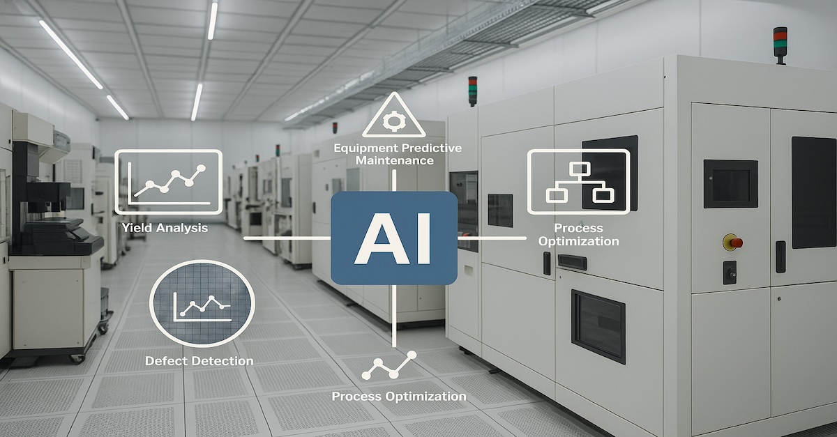
    Semiconductor Agents are AI model-driven assistants built to support the digital stages of chip development across design, verification, optimization, and analysis. Unlike traditional automation scripts or rule-based flows, these agents use large models trained on RTL, constraints, waveforms, logs, and tool interactions.

    This gives them the ability to interpret engineering intent, reason about complex design states, and take autonomous actions across EDA workflows. In practical terms, they act as specialized digital coworkers that help engineers manage work that is too large, too repetitive, or too interconnected for manual execution.

    In design, these agents can generate RTL scaffolds, build verification environments, explore architectural tradeoffs, analyze regression failures, and recommend PPA improvements. In verification, they generate tests, identify coverage gaps, diagnose failure signatures, and run multi-step debug sequences. In physical design, they assist with constraint tuning, congestion analysis, timing closure, and design space exploration by using model-driven reasoning to evaluate large option spaces much faster than human iteration.

    Put simply, model-driven semiconductor agents are intelligent systems that accelerate, improve accuracy, and scale chip development. They convert slow, script-heavy engineering loops into guided, automated workflows, representing a significant shift in how modern silicon will be created.


    Are These Agents Real Or Hype?

    Model-driven semiconductor agents are no longer a future idea. They are already used in modern EDA platforms, where they automate tasks such as RTL generation, testbench creation, debug assistance, and design optimization.

    These agents rely on large models trained on engineering data, tool interactions, and prior design patterns, which allows them to operate with a level of reasoning that simple scripts cannot match.

    Academic research supports this progress. For example, one paper (“Proof2Silicon: Prompt Repair for Verified Code and Hardware Generation via Reinforcement Learning”) reports that using a reinforcement-learning guided prompt system improved formal verification success rates by up to 21% and achieved an end-to-end hardware synthesis success rate of 72%.

    another study (“ASIC‑Agent: An Autonomous Multi‑Agent System for ASIC Design with Benchmark Evaluation”) the authors introduce a sandboxed agent architecture that spans RTL generation, verification, and chip integration, demonstrating meaningful workflow acceleration.

    These research-driven examples show that model-driven and agent-based methods are moving beyond concept toward applied results in chip design.

    It is still early, and no single agent can design a full chip. Human engineers guide decisions, verify results, and manage architectural intent. But the momentum is real. Model-driven semiconductor agents are practical, maturing quickly, and steadily becoming an essential part of how the industry will design and verify chips at scale.


    How Semiconductor Agents Integrate Into the Silicon Lifecycle

    In early design exploration, a semiconductor agent could take a natural-language module description and generate an initial RTL draft along with interface definitions and bare assertions. Engineers would then refine the output instead of starting from a blank file. This reduces time spent on boilerplate RTL and allows teams to explore architectural directions more quickly and with less friction.

    During verification, an agent could analyze regression results, classify failures based on patterns in signals and logs, and propose a minimal reproduction test. This turns hours of manual waveform inspection into a short, actionable summary. Engineers receive clear guidance on where a failure originated and why it may be happening, which shortens debug cycles and helps verification progress more consistently.

    Stage of LifecyclePossible Agent Use CaseWhat The Agent Can DoValue to Engineering Teams
    DesignRTL Draft GenerationConverts written specifications into initial RTL scaffolds and interface definitionsFaster architecture exploration and reduced boilerplate coding
    DesignConstraint & Architecture SuggestionsAnalyzes goals and proposes timing, power, or area tradeoff optionsHelps evaluate design alternatives quickly
    VerificationAutomated Testbench GenerationBuilds UVM components, assertions, and directed tests from module descriptionsReduces manual setup time and accelerates early verification
    VerificationRegression Triage & Pattern DetectionClassifies failures, identifies recurring issues, and recommends likely root causesCompresses debug cycles and improves coverage closure
    Physical DesignPPA ExplorationEvaluates multiple constraint and floorplan options using model reasoningNarrows the search space and speeds up timing closure
    Physical DesignCongestion & Timing AnalysisPredicts hotspots or slack bottlenecks and suggests candidate fixesReduces the number of full P&R iterations
    SignoffIntelligent Rule CheckingIdentifies high-risk areas in timing, IR drop, or design-for-test based on learned patternsHelps engineers prioritize review efforts
    Product EngineeringAnomaly Detection in Pre-Silicon DataAnalyzes logs, waveform summaries, or DFT patterns to detect inconsistenciesImproves first-silicon success probability
    System Bring-UpIssue LocalizationInterprets bring-up logs and suggests potential firmware or hardware mismatchesShortens early debug during lab validation

    In physical design, an agent could evaluate many constraints and floorplan variations using model-driven reasoning. By analyzing congestion signatures, timing slack, and area tradeoffs, it could narrow the design space to a few strong candidates. Engineers would then focus on validating these options rather than manually exploring hundreds of combinations, thereby improving both the speed and the quality of timing closure.


    Who Is Building Semiconductor Agents And What It Takes

    EDA vendors and a new generation of AI-EDA startups are primarily developing semiconductor agents. Established tool providers are adding large models into their design and verification platforms, while startups are building agent-first workflows for RTL, verification, and debug. These systems sit on top of existing EDA engines and aim to reduce repetitive engineering work.

    Building these agents requires deep domain data and strong tool integration. Helpful agents depend on RTL datasets, constraints, logs, waveforms, and optimization traces. They also need alignment layers that help the model understand engineering intent and connect reliably to commercial EDA tools, enabling execution of multi-step flows.

    CategoryWho Is Building ThemWhat They ContributeWhat It Takes to Build Agents
    EDA VendorsEstablished design-tool providersAgent-assisted RTL, verification, debugLarge datasets, tight EDA integration, safety guardrails
    AI-EDA StartupsModel-focused EDA companiesMulti-agent workflows and rapid innovationProprietary models and close customer iteration
    Semiconductor CompaniesInternal CAD and design teamsReal data and domain expertiseAccess to RTL, ECO histories, regressions, waveforms
    Academic LabsUniversities and research centersNew multi-agent methods and algorithmsResearch datasets and algorithm development

    Trust and correctness are central to building these agents. Because chip design errors are costly, teams need guardrails, human oversight, and verifiable outputs. Agents must behave predictably and avoid changes that violate timing, physical, or functional rules.

    In summary, semiconductor agents are being built by organizations with the correct data, EDA expertise, and safety practices. Creating them requires large models, strong domain alignment, and deep integration with existing tools, and these foundations are now driving their rapid adoption.


  • The Case For Building AI Stack Value With Semiconductors

    Image Generated Using DALL·E


    The Layered AI Stack And The Semiconductor Roots

    Artificial intelligence operates through a hierarchy of interdependent layers, each transforming data into decisions. From the underlying silicon to the visible applications, every tier depends on semiconductor capability to function efficiently and scale economically.

    The AI stack can be imagined as a living structure built on four essential layers: silicon, system, software, and service.

    Each layer has its own responsibilities but remains fundamentally connected to the performance and evolution of the chips that power it. Together, these layers convert raw computational potential into intelligent outcomes.

    At the foundation lies the silicon layer, where transistor innovation determines how many computations can be executed per joule of energy. Modern nodes, such as those at 5 nm and 3 nm, make it possible to create dense logic blocks, high-speed caches, and finely tuned interconnects that form the core of AI compute power.

    AI Stack LayerExample TechnologiesSemiconductor Dependence
    SiliconLogic, memory, interconnectsDetermines compute density, power efficiency, and speed
    SystemBoards, servers, acceleratorsDefines communication bandwidth, cooling, and energy distribution
    SoftwareFrameworks, compilers, driversConverts algorithmic intent into hardware-efficient execution
    ServiceCloud platforms, edge inference, APIsScales models to users with predictable latency and cost

    Above this, the system layer integrates the silicon into servers, data centers, and embedded platforms. Thermal design, packaging methods, and signal integrity influence whether the theoretical performance of a chip can be achieved in real-world operation.

    Once silicon is shaped into functional systems, software becomes the crucial bridge between mathematical models and physical hardware. Frameworks such as TensorFlow and PyTorch rely on compilers like XLA and Triton to organize operations efficiently across GPUs, CPUs, or dedicated accelerators. When these compilers are tuned to the architecture of a given chip, its cache size, tensor core structure, or memory hierarchy, the resulting improvements in throughput can reach 30-50 percent.

    At the top of the stack, the service layer turns computation into practical value. Cloud APIs, edge inference platforms, and on-device AI engines rely on lower layers to deliver low-latency responses at a global scale. Even a modest reduction in chip power consumption, around ten percent, can translate into millions of dollars in savings each year when replicated across thousands of servers.

    In essence, the AI stack is a continuum that begins with electrons moving through transistors and ends with intelligent experiences delivered to users. Every layer builds upon the one below it, transforming semiconductor progress into the computational intelligence that defines modern technology.


    Image Credit: The 2025 AI Index Report Stanford HAI

    AI Value From Transistors To Training Efficiency

    The value of artificial intelligence is now measured as much in terms of energy and computational efficiency as in accuracy or scale. Every improvement in transistor design directly translates into faster model training, higher throughput, and lower cost per operation. As process nodes shrink, the same watt of power can perform exponentially more computations, reshaping the economics of AI infrastructure.

    Modern supercomputers combine advanced semiconductors with optimized system design to deliver performance that was previously unimaginable.

    The table below illustrates how leading AI deployments in 2025 integrate these semiconductor gains, showing the connection between chip architecture, energy efficiency, and total compute output.

    AI Supercomputer / ProjectCompany / OwnerChip TypeProcess NodeChip QuantityPeak Compute (FLOP/s)
    OpenAI / Microsoft – Mt Pleasant Phase 2OpenAI / MicrosoftNVIDIA GB2005 nm700 0005.0 × 10¹⁵
    xAI Colossus 2 – Memphis Phase 2xAINVIDIA GB2005 nm330 0005.0 × 10¹⁵
    Meta Prometheus – New AlbanyMeta AINVIDIA GB2005 nm300 0005.0 × 10¹⁵
    Fluidstack France Gigawatt CampusFluidstackNVIDIA GB2005 nm500 0005.0 × 10¹⁵
    Reliance Industries SupercomputerReliance IndustriesNVIDIA GB2005 nm450 0005.0 × 10¹⁵
    OpenAI Stargate – Oracle OCI ClusterOracle / OpenAINVIDIA GB3003 nm200 0011.5 × 10¹⁶
    OpenAI / Microsoft – AtlantaOpenAI / MicrosoftNVIDIA B2004 nm300 0009.0 × 10¹⁵
    Google TPU v7 Ironwood ClusterGoogle DeepMind / Google CloudGoogle TPU v74 nm250 0002.3 × 10¹⁵
    Project Rainier – AWSAmazon AWSAmazon Trainium 27 nm400 0006.7 × 10¹⁴
    Data Source: Epoch AI (2025) and ML Hardware Public Dataset

    From these figures, it becomes clear that transistor scaling and system integration jointly determine the value of AI. Each new semiconductor generation improves energy efficiency by roughly forty percent, yet the total efficiency of a supercomputer depends on how well chips, networks, and cooling systems are co-optimized.

    The GB300 and B200 clusters, built on advanced 3nm and 4nm processes, deliver near-exponential performance per watt compared to earlier architectures. Meanwhile, devices such as Amazon Trainium 2, based on a mature 7nm node, sustain cost-effective inference across massive cloud deployments.

    Together, these systems illustrate that the future of artificial intelligence will be shaped as much by the progress of semiconductors as by breakthroughs in algorithms. From mature 7 nm inference chips to advanced 3 nm training processors, every generation of silicon adds new layers of efficiency, capability, and intelligence.

    As transistors continue to shrink and architectures grow more specialized, AI value will increasingly be defined by how effectively hardware and design converge. In that sense, the story of AI is ultimately the story of the silicon that powers it.


  • The Convergence Of Chiplets And AI In Semiconductor Design

    Image Generated Using 4o


    The semiconductor industry is at an inflection point. For decades, the trajectory of Moore’s Law provided a predictable path forward: smaller transistors, higher performance, and lower costs. But as I discussed in The More Than Moore Semiconductor Roadmap, shrinking nodes alone can no longer sustain the pace of progress. Physical and economic limits are forcing the industry to seek new strategies that redefine what advancement means in this post-Moore era.

    Two of the most important forces reshaping the landscape are chiplets and artificial intelligence.

    Chiplets provide modularity, efficiency, and flexibility in system design, while AI is driving entirely new computational demands and design paradigms. Each of these trends is powerful on its own, but their true potential emerges when considered together. The convergence of chiplets and AI is setting the foundation for how future semiconductors will be conceived, validated, and manufactured.


    Why Chiplets And AI

    Chiplets break down large monolithic SoCs into smaller, reusable building blocks that can be integrated within a package. This approach reduces reticle size constraints, improves yield, and allows system designers to mix different process nodes and IP blocks. As explained in The Rise of Semiconductor Ghiplets, modularity is not just about performance scaling but also about lowering costs and accelerating time to market.

    AI, on the other hand, is creating workloads that are unprecedented in size and complexity. Training neural networks with billions of parameters requires not just raw compute power, but also immense memory bandwidth, efficient data movement, and specialized accelerators.

    These demands are increasingly challenging to meet with monolithic designs. Chiplets solve this by allowing designers to integrate AI accelerators, memory dies, and I/O blocks within the same package, scaling systems in ways monolithic chips cannot.

    The relationship is symbiotic. AI workloads need chiplets for modular scalability, while chiplets need AI to push the development of advanced architectures, packaging, and simulation tools that can handle the complexity of integration.


    AI Needing New Chiplet Based Architecture

    The rapid scaling of AI models has exposed the limitations of traditional semiconductor design. As explored in The Hybrid AI and Semiconductor Nexus, AI is forcing the industry to rethink architectures around data movement, memory hierarchies, and workload-specific optimization. Monolithic SoCs struggle to deliver the balance of compute and bandwidth that AI requires.

    Chiplet-based architectures solve this by enabling heterogeneous integration. A single package can combine logic dies manufactured on cutting-edge nodes with memory chiplets on mature nodes and I/O dies optimized for high-speed connectivity. This modularity allows for greater flexibility in designing AI accelerators tailored to specific workloads, whether in data centers, edge devices, or mobile platforms.

    Industry standards like UCIe are accelerating this shift by providing open, vendor-neutral interconnects that make chiplet ecosystems interoperable. This means AI hardware development no longer needs to rely on closed, vertically integrated designs, but can instead draw from an ecosystem of interoperable components. Without chiplets, scaling AI hardware efficiently would be economically unsustainable.


    Bottleneck For AI And Chiplets To Grow Together

    Despite the promise, the convergence of chiplets and AI faces significant bottlenecks. Packaging complexity is one of the most pressing. High-speed die-to-die interconnects must be validated for signal integrity across process, voltage, and temperature corners. In 2.5D and 3D packages, thermal gradients create hotspots that impact performance and reliability. Mechanical stresses from advanced packaging compounds must also be modeled to avoid long-term failures. These are not trivial extensions of SoC verification, but entirely new domains of system-level engineering.

    Yield is another critical constraint. As I explained in The Economics of Semiconductor Yield, profitability in semiconductors depends heavily on how many functional dies come off a wafer. With chiplets, the probability of system-level failure increases since multiple dies must work together flawlessly. A defect in one chiplet can compromise an entire package, multiplying yield risks. This is why embedding yield optimization into the design process is so essential.

    Finally, simulation and validation remain major bottlenecks. As noted in The Role of Simulation in Semiconductor Product Development, traditional EDA flows were not designed to handle chiplet-level interactions. AI-driven simulation, as I explored in The Semiconductor Data Driven Decision Shift, offers a path forward. However, the industry is still in the early stages of building predictive, adaptive simulation environments capable of handling such complexity.


    The convergence of chiplets and AI is not a coincidence but a necessity. AI workloads demand architectures that can only be delivered through modular chiplet design. At the same time, chiplets require the intelligence and predictive power of AI-driven simulation to overcome integration and yield challenges.

    As I discussed in The Semiconductor Learning Path, success in the post-Moore era requires connecting design, manufacturing, and data into a unified roadmap. Chiplets and AI are two of the most critical pillars in this roadmap, and their convergence is redefining how the industry balances complexity, cost, and scalability.

    The companies that master this interplay will not only meet the demands of today’s AI workloads but also shape the semiconductor roadmaps of the next decade. The future of design is modular, data-driven, and inseparable from the intelligence that AI brings to every stage of the value chain.


  • The Rise Of AI Co-Creativity In Semiconductor Productization

    Image Generated Using 4o


    AI As A Creative Partner In Chip Design

    Chip design has always been a demanding discipline, requiring engineers to balance performance, power, and area across endless iterations. Traditionally, much of this work has been manual and time-consuming. With the rise of large language models, engineers now have intelligent collaborators at their side.

    Recent research demonstrates how these models can take natural language specifications, such as “design a 4-bit adder,” and generate corresponding Verilog code that is both syntactically correct and functionally accurate.

    Projects like VerilogEval and RTLLM highlight how LLMs can handle structured hardware description, while experiments such as ChipGPT allow engineers to ask why a module fails verification and receive context-aware debugging suggestions.

    These capabilities are not about replacing human designers, but about extending their reach. The engineer provides intent and creative direction, while AI manages repetitive exploration, expanding the possibilities of what can be achieved in each design cycle.


    Image Credit: OpenLLM-RTL

    Flexible Architectures For A Rapidly Evolving Landscape

    The impact of AI co-creativity extends beyond the design process into the way chips themselves are architected. Traditional fixed-function hardware often struggles to remain relevant as AI models evolve, since a design optimized for one generation of algorithms may quickly become outdated.

    AI-enabled frameworks such as AutoChip and HiVeGen are addressing this challenge by automatically generating modular and reconfigurable hardware. Instead of starting over for each new workload, AI adapts existing modules to meet new requirements.

    This makes it possible to create architectures that behave more like flexible platforms than static end products, evolving alongside the software they are built to support.

    Such adaptability reduces the risk of obsolescence, lowers redesign costs, and ensures that semiconductors keep pace with the rapid cycles of algorithmic change.


    Image Credit: CorrectBench

    Why AI Co-Creativity Matters

    The practical benefits of AI as a co-creator are felt across the entire productization cycle. Multi-agent systems such as AutoEDA demonstrate that large portions of the RTL-to-GDSII flow can be automated, with agents specializing in tasks like synthesis, placement, and verification before combining their results into a complete design.

    By mirroring the way human teams distribute responsibilities, these systems drastically shorten time-to-market. Designs that once took months to finalize can now be completed in weeks, allowing faster response to industry demands.

    Quality also improves when AI is embedded in the flow. Benchmarks such as CorrectBench illustrate that LLMs are capable of generating verification testbenches with high functional coverage, reducing the burden on engineers and improving design reliability. Similarly, AI-driven defect detection in layout generation helps identify issues early in the process, preventing costly downstream corrections.

    These capabilities enable engineers to concentrate on strategic architectural decisions and system-level innovation, knowing that AI can handle the lower-level repetitive work.


    Image Credit: EDAid

    An Expanding Ecosystem Of Co-Creativity

    The reach of AI is spreading across the semiconductor ecosystem. Conversational assistants like LLM-Aided allow engineers to interact with tools in natural language, reducing the steep learning curve often associated with complex design environments.

    Code and script generation tools, such as those explored in ChatEDA, EDAid, and IICPilot, produce automation scripts for synthesis and verification, eliminating the need for repetitive manual scripting.

    Multi-agent frameworks go further, creating distributed AI systems in which specialized agents collaborate to carry an entire design from high-level specification to implementation.

    These developments point toward an ecosystem where human engineers and AI systems are intertwined at every stage of productization. Instead of siloed and linear workflows, semiconductor development becomes a dynamic collaboration in which human creativity and machine intelligence reinforce one another.


  • The Use Cases Of AI In Semiconductor Industry

    Image Generated Using 4o


    Why AI Matters In The Semiconductor Industry

    Earlier this week, I had the opportunity to deliver a session at Manipal University Jaipur as part of their Professional Development Program on AI-Driven VLSI Design and Optimization. The event brought together students, researchers, and professionals eager to explore how Artificial Intelligence is reshaping the semiconductor landscape.

    During this talk, we dove deep into the real-world applications of AI in semiconductor design, verification, and manufacturing. We discussed why AI is not just a buzzword but an increasingly essential tool to tackle the industry’s enormous complexity and relentless pace of innovation.

    We all know that semiconductors are the invisible workhorses of our digital world. Every smartphone you use, car you drive, or cloud service you rely on depends on tiny silicon chips built with extraordinary precision. Yet designing and manufacturing those chips has become one of the most challenging engineering tasks of our time.

    Traditionally, semiconductor development involves painstaking manual work and countless iterations. Engineers grapple with vast datasets, strict design rules, and manufacturing tolerances measured in nanometers. A single error can mean millions of dollars in wasted wafers, delays, or product recalls.

    This is where AI comes in, not to replace engineers but to empower them.

    AI offers transformative advantages for the semiconductor industry, such as:

    • Accelerating Design Cycles: Automating tasks like layout, simulation, and code generation
    • Improving Yields: Detecting subtle defect patterns and predicting manufacturing outcomes
    • Enhancing Efficiency: Fine-tuning fab operations and preventing costly equipment failures
    • Reducing Costs: Minimizing errors, rework, and scrap, which all contribute to faster time-to-market

    However, AI is not a silver bullet. It still requires high-quality data, domain expertise, and human oversight to deliver meaningful results. Each challenge in semiconductor design or manufacturing often demands custom AI approaches rather than generic solutions.

    Ultimately, AI matters because it helps engineers navigate the staggering complexity of modern chip development, enabling faster innovation and higher-quality products.


    Image Credit: Chetan Arvind Patil

    Two Big Perspectives: AI In Versus AI For Semiconductors

    When we talk about AI and semiconductors, there are two equally important perspectives:

    • AI in Semiconductors: How AI is used as a tool inside the semiconductor industry
    • AI for Semiconductors: How semiconductors are explicitly built to power AI applications

    The table below summarizes the differences:

    AspectAI In SemiconductorsAI For Semiconductors
    Main RoleAI helps improve how chips are designed, manufactured, and testedChips are designed specifically to run AI workloads faster and more efficiently
    Key Benefits– Faster design cycles
    – Improved yields
    – Predictive maintenance
    – Cost reduction
    – High-speed AI processing
    – Energy efficiency for AI tasks
    – Enables new AI-driven applications
    Typical Use Cases– AI-driven EDA tools
    – Defect detection
    – Test data analytics
    – Fab process optimization
    – GPUs and TPUs
    – Custom AI accelerators (ASICs)
    – AI-specific memory (HBM)
    – Chiplets for AI performance
    Industry FocusImproving internal semiconductor workflows and efficiencyCreating products for AI markets such as cloud, edge computing, automotive, etc.
    Impact on IndustrySpeeds up semiconductor development and manufacturingPowers the broader AI revolution in multiple industries


    These two perspectives are deeply connected. For example:

    • AI tools help design AI accelerators faster and more efficiently
    • AI hardware built by semiconductor firms enables the massive computations needed for AI software used in semiconductor manufacturing

    In essence, AI is improving how we build chips, and better chips are enabling ever more powerful AI. It is a cycle that is driving both technological progress and new business opportunities across the industry.


    Practical AI Use Cases Across The Semiconductor Lifecycle

    AI is not just a futuristic concept. It is already hard at work in real, practical ways throughout the semiconductor industry. From how engineers design and verify chips to how fabs manufacture silicon wafers and analyze test results, AI is becoming deeply woven into the fabric of semiconductor workflows.

    Unlike traditional methods that often rely on manual effort and painstaking trial-and-error, AI brings speed, predictive power, and the ability to uncover hidden patterns in massive datasets. This makes it an invaluable partner for tackling challenges like complex design rules, defect detection, process optimization, and yield improvement.

    Whether it is accelerating chip design with natural-language tools, optimizing manufacturing parameters in real-time, or spotting subtle defects invisible to human eyes, AI is helping semiconductor companies work smarter and faster. Let us explore how these applications play out across the semiconductor lifecycle, from initial design all the way to manufacturing and testing.

    Here is a snapshot of where AI is making its mark:

    Lifecycle StageAI Use CasesBenefits
    Design– Natural language to HDL code (e.g. ChipGPT)
    – Design-space exploration- PPA optimization
    Faster design cycles, reduced manual coding
    Verification– Auto-generation of testbenches (e.g. LLM4DV)
    – Functional coverage analysis
    Shorter verification times, higher confidence in chip functionality
    Layout– AI-assisted layout tools (e.g. ChatEDA)
    – Placement and routing suggestions
    Accelerates physical design, reduces errors
    Manufacturing (FAB)– Computational lithography (e.g. cuLitho)
    – Process parameter optimization- Predictive maintenance
    Higher yield, fewer defects, lower manufacturing costs
    Testing & Yield– Test data analytics
    – Defect pattern detection
    – Root-cause analysis
    Improved test coverage, faster debug, yield enhancement

    Across the lifecycle, AI is stepping in to tackle some of the industry’s most complex challenges. In design, tools like ChipGPT are translating natural-language specifications directly into Verilog code, helping engineers move from ideas to functional designs with remarkable speed. In verification, AI models can auto-generate testbenches and assertions, reducing the manual burden and ensuring higher functional coverage, traditionally one of the biggest bottlenecks in chip development.


    Image Credit: Chetan Arvind Patil and ChipGPT Paper

    Manufacturing has seen dramatic gains from AI-driven computational lithography. For example, platforms like cuLitho use GPUs to accelerate complex optical proximity correction (OPC) calculations, essential for creating accurate masks at advanced nodes like 5nm or 3nm. Meanwhile, in testing and yield analysis, machine learning is analyzing huge volumes of test data, detecting defect patterns, and predicting yield outcomes, allowing fabs to tweak processes proactively and avoid costly rework.


    Image Credit: Chetan Arvind Patil and NVIDIA

    Overall, these advances are not only saving time and costs but are also enabling engineers to push the boundaries of innovation. AI has become more than a tool, it is an integral partner that helps the semiconductor industry keep pace with rising complexity and shrinking timelines.


    Building AI Skills For Semiconductor Professionals

    As AI becomes increasingly embedded in semiconductor workflows, professionals across the industry need to level up their skills. The good news? You do not have to become a data scientist to thrive in this new era. But understanding how AI fits into the semiconductor ecosystem and how to work alongside it, is quickly becoming essential.

    Semiconductor engineers, designers, and technologists should focus on practical, applied knowledge rather than deep AI theory. Here is what matters most:


    Ultimately, building AI skills is not about replacing your core semiconductor expertise. It is about augmenting it. AI tools can handle repetitive analysis, crunch massive datasets, and suggest optimizations that would take humans days or weeks to discover. But it is still engineers who guide the work, validate results, and make critical decisions.

    In this evolving landscape, those who understand both semiconductors and AI will be uniquely positioned to drive innovation, solve complex challenges, and shape the future of the industry.


    The Road Ahead: AI As A Partner, Not A Replacement

    As the semiconductor industry pushes forward, it is clear that AI will play an essential role. But despite the hype, AI is not here to replace engineers, and it is here to work alongside them.

    From generating chip designs based on natural-language prompts to predicting manufacturing issues before they happen, AI is becoming an intelligent assistant that makes complex tasks faster and more precise.

    Yet, AI is not magic. It still needs clean, high-quality data and human expertise to interpret results and make decisions. There is no single AI solution that fits every challenge in semiconductors. Engineers remain critical for guiding AI tools, validating outputs, and handling situations where nuance and domain knowledge are essential.

    Looking ahead, the most successful professionals will be those who learn to collaborate with AI, using it to tackle complexity and unlock new opportunities. In the semiconductor industry, AI will not replace human ingenuity, it will amplify it, driving faster innovation and helping us solve problems once thought impossible.


  • The Implication Of AI Revolution On Semiconductor Industry

    Image Generated Using 4o


    AI Workloads Redefine Chip Architecture

    AI workloads are fundamentally different from traditional computing tasks. Where classic CPUs focused on serial instruction execution, AI models and intense neural networks demand massive parallelism and high data throughput. This has driven a shift toward specialized compute architectures, such as GPUs, tensor processors, and custom AI ASICs. These designs move away from pure von Neumann principles, emphasizing data locality and minimizing costly data movement.

    At the heart of this shift is the need to process billions of operations efficiently, for which the traditional architectures struggle to meet AI’s bandwidth and memory requirements, leading designers to adopt local SRAM buffers, near-memory compute, and advanced interconnects. However, these improvements come at the cost of larger die areas, power density challenges, and significant NRE costs, particularly on advanced nodes.

    For customers, these changes present both opportunities and risks. Custom AI silicon offers significant performance and power advantages, but it requires deep expertise in hardware-software co-design and substantial upfront investments. While hyperscalers and large OEMs pursue custom ASICs for competitive differentiation, smaller players often remain on general-purpose GPUs to avoid high development costs and longer time-to-market.

    Ultimately, AI workloads are reshaping not only chip architectures but the economics of semiconductor design. The rapid pace of AI model evolution forces designers to iterate through silicon cycles at a high frequency, placing immense pressure on design teams, foundries, and the entire supply chain. While the industry stands to benefit enormously from AI-driven demand, it must navigate growing complexity, power limits, and escalating costs to deliver sustainable innovation in the years ahead.

    Impact On Process Nodes And Technology Roadmaps

    AI has also become a significant force shaping process technology roadmaps. Unlike previous drivers, such as mobile or standard compute, AI accelerators require enormous compute density and power efficiency. Advanced nodes, ranging from 7nm to 2nm, are attractive because they offer higher transistor performance, improved energy efficiency, and increased integration capabilities, all of which are critical for massive AI workloads.

    However, these benefits come with significant trade-offs, including escalating design costs, more complex manufacturing, and tighter control over variability.

    NodeKey AI BenefitsMain ChallengesTypical AI Use Cases
    7nmGood density and performance; mature yieldsPower still high for very large chipsMid-size AI accelerators, edge AI SoCs
    5nmBetter energy efficiency; higher transistor countRising mask costs; increased design rules complexityHigh-performance inference, initial LLM training
    3nmSignificant performance gains; lower powerYield variability; extreme design complexityLarge AI ASICs, data center accelerators
    2nmAdvanced gate structures (nanosheet/GAA); excellent scalingImmature yields; highest costs; thermal densityCutting-edge AI training, future LLM architectures

    These technology nodes are crucial enablers for achieving AI performance targets, but they also exponentially increase costs. Mask sets touches million at 3nm and beyond, making custom AI silicon viable only for companies with significant scale or unique workloads. At the same time, the physical limits of power density mean that merely shrinking transistors is not enough. Advanced cooling, power delivery networks, and co-optimized software stacks are now mandatory to fully realize the benefits of smaller nodes.

    As a result, the AI revolution is not just accelerating node transitions but fundamentally changing how companies think about chip design economics. To tackle this, the industry is moving toward chiplet architectures, heterogeneous integration, and tight hardware-software codesign to balance performance gains against skyrocketing complexity and costs.

    Overall, AI is no longer simply an application. It is also shaping the entire technology roadmap for the semiconductor industry.

    Supply Chain And Manufacturing Pressure

    The AI boom has also exposed significant bottlenecks across the semiconductor supply chain. Unlike typical semiconductor products, AI accelerators are extremely large, power hungry, and require advanced packaging and memory technologies. These characteristics have placed unprecedented strain on fabrication capacity, substrate availability, advanced packaging lines, and test infrastructure.

    The global shortages of GPUs over the past two years are a direct consequence of these constraints, compounded by the explosive demand for AI and limited manufacturing flexibility for such specialized devices.

    Supply Chain AreaAI-Driven ChallengesImpacts
    Foundry CapacityAI chips demand leading-edge nodes (5nm, 3nm), consuming large die areas and reticle-limited designs.Limited wafer starts for other segments; long lead times; higher wafer costs.
    Substrate ManufacturingLarge interposers needed for chiplets and HBM; organic substrate capacity under strain.Shortages of ABF substrates; increased substrate costs; delivery delays.
    Advanced Packaging2.5D/3D integration (e.g. CoWoS, Foveros) essential for AI chips.OSAT capacity constrained; long cycle times; thermal and yield challenges.
    Testing InfrastructureLarge AI devices have complex test vectors; high power complicates burn-in and functional test.Longer test times; increased test costs; limited availability of high-power ATE equipment.
    HBM Memory SupplyAI accelerators increasingly rely on HBM2e, HBM3; production is concentrated among few vendors.Supply constraints limit AI chip output; significant cost increases for HBM stacks.
    Equipment AvailabilityEUV lithography tools are limited in number and expensive to deploy.Throughput constraints slow ramp of advanced nodes; high capital requirements.
    EDA Tool ScalabilityAI chip designs are extremely large (hundreds of billions of transistors).Longer place-and-route times; higher tool licensing costs; increased verification complexity.
    Material Supply ChainAdvanced processes require ultra-pure chemicals and specialty materials.Vulnerable to geopolitical risks; localized shortages can halt production.

    Foundry capacity has become a significant bottleneck for AI chips, which often require large die sizes close to reticle limits. These large designs consume significant wafer starts, increasing defect risks, yield challenges, and lead times, while driving higher costs and capacity reservations from major AI players.

    Advanced packaging is equally strained. AI designs rely on chiplets and high-bandwidth memory stacked with interposers, requiring complex processes such as CoWoS and Foveros. Substrate shortages and specialized test needs further slow production, as large AI chips require high power handling and complex validation.

    Overall, AI has exposed deep vulnerabilities in semiconductor manufacturing. Without significant expansion in lithography, packaging, and test capacity, these bottlenecks will continue to constrain the speed at which AI solutions can reach the market, impacting their cost and availability.

    Long-Term Implications For Industry Economics And Design

    AI is also fundamentally transforming how the semiconductor industry thinks about both business economics and technical design. Unlike traditional markets like mobile or PCs, which relied on massive volumes to justify advanced-node costs, AI silicon often serves lower-volume segments with extremely high chip complexity and premium pricing.

    This disrupts the traditional model of spreading non-recurring engineering (NRE) costs over millions of units and forces companies to weigh the risks and rewards of investing in custom hardware for rapidly evolving AI workloads.

    The net result is an industry facing higher costs, faster technical cycles, and the need for closer collaboration between silicon engineers and AI software teams. While AI promises significant new opportunities, it also raises the stakes for semiconductor companies, demanding greater agility, investment, and technical depth to remain competitive in this rapidly shifting landscape.


  • The Role Of AI In Semiconductor Manufacturing: Fact Or Fiction

    Image Generated Using DALL-E


    The AI Debate

    Artificial Intelligence (AI) often sparks divided opinions as a groundbreaking innovation or technological hype.

    At the same time, in semiconductor manufacturing, where billions of dollars depend on minuscule yield and efficiency gains, the industry must critically evaluate whether AI delivers transformative results or is merely overblown. Semiconductor FABs and OSATs globally are already investing heavily in AI-driven solutions, leveraging predictive maintenance to reduce equipment downtime, AI-powered Automated Optical Inspection (AOI) to reliably detect subtle defects in packaging, and adaptive testing to reduce costs without compromising quality.

    Despite these promising outcomes, it is important to remain realistic. Claims of fully autonomous fabs or entirely self-driving manufacturing environments are exaggerated. While AI significantly enhances productivity and quality, semiconductor manufacturing relies fundamentally on skilled engineers to interpret AI insights, make strategic decisions, and integrate these technologies into existing systems. Thus, AI’s genuine value is clear, but only if deployed with measured expectations, careful validation, and thoughtful integration strategies.


    Is AI Integration A Necessity In Semiconductor Manufacturing?

    While labeling AI indispensable due to its popularity is tempting, a critical examination still reveals a nuanced picture. Semiconductor manufacturing thrived long before AI, achieving innovation through rigorous engineering, strict quality control, and methodical experimentation.

    Thus, it is fair to ask whether AI is necessary or merely another technological “nice-to-have”?

    Let Us Understand Why Skepticism Is Valid: AI is powerful but brings complexities, high integration costs, demanding data requirements, and organizational barriers. Traditional methods may remain sufficient and economically practical for fabs running mature or legacy processes (e.g., analog or 130nm+ nodes). Additionally, reliance on AI without adequate expertise or infrastructure can lead to confusion, causing AI-generated insights to be misunderstood and potentially harming operational efficiency.

    How AI Can Be Essential In Semiconductor Manufacturing: Despite valid skepticism, the necessity of AI becomes unmistakable when viewed through the lens of today’s leading-edge semiconductor processes. AI integration is becoming necessary due to the staggering complexity at advanced nodes (7nm, 5nm, 3nm, and beyond), complex packaging technologies, and the need for exact manufacturing tolerances.


    Cost Of Deploying AI In Semiconductor Manufacturing

    Deploying AI in semiconductor manufacturing offers substantial benefits, such as enhanced yield, reduced downtime, and improved efficiency. However, these advantages require significant upfront and ongoing investments. Costs depend heavily on fab size, technology node, and existing infrastructure.

    Infrastructure-related investments typically include powerful GPUs, specialized AI accelerators, cloud or edge computing, robust data storage, and networking infrastructure for real-time analytics. AI software licensing, often from commercial platforms or customized proprietary solutions, also represents a substantial cost component.

    Data preparation and integration also add notable expenses, as AI requires clean, labeled, and integrated data. Labor-intensive processes such as data labeling, cleaning, and system integration across MES, test equipment, and legacy infrastructure further increase costs.

    Cost ComponentEstimated Cost (USD)
    AI Hardware Infrastructure$500K – $2M
    AI Software Licensing And Tools$200K – $1M annually
    AI Data Integration And Preparation$200K – $500K
    AI Talent Acquisition And Training$300K – $1M annually
    Annual Maintenance And Operations Of AI$100K – $400K annually
    Total First-Year Costs~$1.3M – $4.9M
    Sources: Industry Reports

    Deploying AI also demands significant investment in talent acquisition and workforce training. Companies must hire specialized AI/ML engineers and data scientists,. Training for existing engineers and operational staff is also critical to ensure effective AI system use and maintenance, which is another adder.

    Additionally, AI systems involve ongoing operational costs such as model retraining, software updates, license renewals, and regular infrastructure maintenance. These recurring expenses typically amount to 10–20% of the initial investment annually, highlighting the sustained financial commitment necessary for successful AI implementation.


    Takeaway

    Deploying AI in semiconductor manufacturing demands considerable upfront and ongoing investments in infrastructure, software, data management, and skilled talent. However, as semiconductor manufacturing complexity increases at advanced technology nodes, AI integration is shifting from beneficial to strategically essential.

    AI-driven solutions consistently deliver improved efficiency, reduced downtime, higher yields, and significant financial gains. To fully capture these benefits, companies must strategically plan their AI deployments, scale thoughtfully, and maintain realistic expectations to achieve sustained profitability and competitive advantage.


  • The Hybrid AI And Semiconductor Nexus

    Image Generated Using DALL-E


    What Is Hybrid AI?

    Hybrid AI represents a paradigm shift in AI architecture. Instead of relying solely on the cloud for processing, hybrid AI distributes computational workloads between cloud servers and edge devices.

    Such an architecture offers numerous benefits:

    • Cost Efficiency: Offloading tasks to edge devices reduces cloud infrastructure expenses
    • Energy Savings: Edge devices consume less energy, minimizing the environmental impact
    • Enhanced Performance: On-device processing reduces latency and ensures reliability, even with limited connectivity
    • Privacy and Personalization: Keeping sensitive data on-device enhances security while enabling more tailored user experiences

    This approach mirrors the historical evolution of computing, transitioning from mainframes to the current blend of cloud and edge capabilities. Hybrid AI, however, demands robust hardware, and that is where semiconductors take center stage.


    Type Of Hybrid AI

    Hybrid AI architectures vary based on how workloads are distributed between cloud and edge devices. These types include:

    Device Hybrid AI: In this model, the edge device primarily processes AI tasks, offloading to the cloud only when necessary. For example, smartphones running lightweight AI models locally ensure fast, reliable responses for tasks like voice assistants or predictive text. This minimizes cloud dependency and enhances privacy while reducing latency.

    Joint Hybrid AI: This approach involves cloud and edge devices working collaboratively to process tasks simultaneously. An everyday use case is autonomous vehicles, where on-device AI handles real-time navigation while cloud services optimize routes. Similarly, generative AI models can generate and refine draft outputs locally using more complex cloud-based models. This model combines cloud scalability with edge efficiency.


      The Semiconductor Role In Hybrid AI

      Semiconductors are the cornerstone of hybrid AI, equipping edge devices with the computational power and energy efficiency needed to execute generative AI workloads. Advanced processors such as NPUs, GPUs, and TPUs are specifically engineered to handle the demanding matrix operations and parallel processing tasks integral to neural network models.

      By enabling local processing of AI models on edge devices, these devices significantly reduce reliance on cloud infrastructure, minimizing latency, enhancing data privacy, and improving user experience. Recent breakthroughs in chip design and integration allow AI models with billions of parameters to run efficiently on mobile devices, showcasing the scalability and sophistication of modern semiconductor technologies.

      These advancements are driven by integrating AI-specific accelerators, optimized instruction sets, and sophisticated power management mechanisms. Features like dynamic scaling, hardware-based quantization, and mixed-precision computing enable high-performance AI computations while maintaining low energy consumption. This synergy of processing capability and efficiency showcases the semiconductor’s transformative role in advancing hybrid AI systems.


      The Future Is Hybrid AI Stack

      The Hybrid AI Stack is the next step in AI, combining the power of cloud computing with the efficiency of edge devices. It seamlessly integrates hardware and software to meet the needs of modern AI applications.

      This stack allows edge devices to run AI models locally using lightweight frameworks, ensuring fast responses and better privacy. Middleware helps manage tasks between the edge and the cloud, sending heavier workloads to the cloud when needed. The cloud layer handles functions like training and updating AI models, keeping edge devices up-to-date without disruption.

      LayerComponents and Key Features
      Hardware LayerCombines advanced edge devices (NPUs, GPUs, TPUs) for on-device AI processing, cloud infrastructure for large-scale training, high-speed 6G networks for seamless edge-cloud communication, and smart sensors for real-time, accurate data collection.
      Firmware LayerIncludes AI-optimized drivers for hardware control, dynamic energy management with advanced DVFS, and lightweight runtimes for real-time, efficient edge inferencing.
      Middleware LayerFeatures intelligent task orchestration to allocate workloads between edge and cloud, resource optimization tools for compute, power, and storage, and universal interoperability frameworks for seamless integration.
      AI Framework LayerProvides edge-centric tools like TensorFlow etc., cloud integration kits for continuous learning, and federated AI models for secure, distributed processing.
      Application LayerPowers real-time applications like AR, voice, and vision on edge devices, industrial AI for predictive and autonomous systems, and hybrid innovations in vehicles, robotics, and healthcare.

      The stack is flexible and scalable, making it applicable across various applications. For example, it enables real-time AI features on smartphones, like voice recognition or photo enhancements and supports industrial systems by combining local analytics with cloud-based insights.

      With this integration, the Hybrid AI Stack offers a simple yet powerful way to bring AI into everyday life and industry, making AI more intelligent, faster, and more efficient.


    1. The State Of AI In Semiconductor Chip Manufacturing

      Image Generated Using DALL-E


      AI And Semiconductor

      The relentless pursuit of miniaturization, speed, and complexity has long defined the semiconductor industry. Driven by Moore’s Law, which predicts that the number of transistors on a chip doubles approximately every two years, this principle has been the cornerstone of semiconductor innovation for decades. However, maintaining this pace has become increasingly difficult due to technological bottlenecks and physical limitations, such as power efficiency, heat dissipation, and material constraints.

      This transformation pushes the industry to explore critical areas using AI:

      1. AI In Semiconductor Design: Automating design workflows to achieve faster time-to-market and lower error rates
      2. Yield Optimization: Leveraging AI to identify defects and improve production efficiency
      3. Manufacturing Automation: Enhancing processes such as lithography, etching, and deposition with precision AI models
      4. Cost Reduction: Using AI to streamline operations and reduce waste, driving profitability
      5. Faster Innovation Cycles: Applying machine learning for predictive analytics, enabling proactive decision-making

      The semiconductor industry’s ability to integrate AI will determine its competitiveness and capacity to meet the demands of a rapidly advancing digital world.


      Research Related To AI In Semiconductor Manufacturing

      Research into AI applications for semiconductor manufacturing is rapidly advancing, focusing on improving process efficiency, defect detection, and predictive maintenance.

      Below are a few examples that summarize AI’s role in semiconductor manufacturing, showcasing innovative ideas, applications, and methodologies that will shape the future of AI in semiconductor manufacturing.

      TitleDescriptionSource
      Applying Artificial Intelligence at Scale in Semiconductor ManufacturingExplores the potential of AI and machine learning to generate significant business value across semiconductor operations, from research and chip design to production and sales.McKinsey & Company
      AI in Semiconductor Manufacturing: The Next S Curve?Discusses the surge in demand for AI and generative AI applications, emphasizing the importance for semiconductor leaders to understand and apply these technologies effectively.McKinsey & Company
      Production-Level Artificial Intelligence Applications in Semiconductor ManufacturingA panel discussion on the use of AI techniques to address production-level challenges in semiconductor manufacturing, highlighting practical applications and solutions.IEEE Xplore
      Advancements in AI-Driven Optimization for Enhancing Semiconductor ManufacturingProvides a comprehensive investigation into how AI is utilized to enhance semiconductor manufacturing processes, offering insights into current methodologies and future research directions.Journal of Scientific and Engineering Research
      A Survey on Machine and Deep Learning in Semiconductor IndustryExamines the integration of machine and deep learning in the semiconductor industry, discussing methods, opportunities, and challenges.SpringerLink
      Explainable AutoML with Adaptive Modeling for Yield Enhancement in Semiconductor Smart ManufacturingProposes an explainable automated machine learning technique for yield prediction and defect diagnosis in semiconductor manufacturing.arXiv
      Universal Deoxidation of Semiconductor Substrates Assisted by Machine Learning and Real-Time Feedback ControlUtilizes a machine learning model to automate substrate deoxidation, aiming to standardize processes across various equipment and materials.arXiv
      SEMI-CenterNet: A Machine Learning Facilitated Approach for Semiconductor Defect InspectionPresents an automated deep learning-based approach for efficient localization and classification of defects in SEM images.arXiv
      Improved Defect Detection and Classification Method for Advanced IC Nodes Using Slicing Aided Hyper Inference with Refinement StrategyInvestigates the use of the Slicing Aided Hyper Inference framework to enhance detection of small defects in semiconductor manufacturing.arXiv
      AI in Semiconductors: Innovations Shaping 2024 and BeyondExplores how AI applications are enabling faster, more efficient manufacturing processes and driving innovations in product design, supply chain management, and predictive maintenance.Infiniti Research

      AI Talent In Semiconductor Manufacturing:

      The rise of AI in semiconductor manufacturing has also created a pressing demand for specialized talent that combines domain expertise in semiconductors with advanced skills in artificial intelligence. Professionals with knowledge of chip design, fabrication processes, and quality control are now expected to work alongside AI tools and algorithms to optimize manufacturing workflows.

      Key roles include data scientists, machine learning engineers, and AI researchers who can develop defect detection, predictive maintenance, and process optimization models. Additionally, cross-disciplinary expertise is essential, as AI implementation requires seamless collaboration between semiconductor engineers and software specialists.

      SkillDescription
      Data Analytics and Statistical ModelingAbility to process and interpret complex datasets generated in semiconductor production.
      Deep Learning and Neural NetworksExpertise in designing algorithms for pattern recognition and anomaly detection.
      Automation and RoboticsKnowledge of automating semiconductor manufacturing workflows to enhance precision and efficiency.
      Process Control SystemsUnderstanding of how to integrate AI with process monitoring and control systems.
      Predictive AnalyticsDeveloping models that anticipate equipment failures and process anomalies before they occur.
      Edge AI ApplicationsImplementing AI at the hardware level for real-time decision-making in fabrication facilities.
      Programming SkillsProficiency in Python, R, TensorFlow, PyTorch, and other AI-focused tools.
      Domain Knowledge in Semiconductor Physics and ProcessesApplying AI in the context of lithography, etching, and deposition.
      Cloud and High-Performance ComputingLeveraging scalable infrastructure for AI model training and deployment.

      As the industry evolves, organizations and talents must invest heavily in skilling programs, partner with academic institutions, and develop tailored training initiatives to bridge the talent gap.

      The need for AI talent in semiconductor manufacturing will not be only about meeting current demands but also about driving future innovation, ensuring that companies stay competitive in a rapidly advancing technological landscape.

      Challenges And Future Directions

      Despite the significant advancements AI brings to wafer fabrication, several challenges remain. One major challenge is integrating AI systems with legacy equipment, which can be difficult due to compatibility issues and the need for significant data infrastructure upgrades.

      Additionally, the quality of AI’s predictions and optimizations heavily depends on the quality and volume of data available, which can be a limiting factor in specific fabrication environments.

      Looking ahead, the future of AI in wafer fabrication will likely involve even more sophisticated models that leverage larger datasets and incorporate advanced sensor technologies. Developing hybrid AI approaches, combining physics-based modeling with machine learning, could also lead to greater accuracy and reliability in process control. Including, more advances in computational lithography.


    2. The State Of AI In Semiconductor Chip Design

      Image Generated Using DALL-E


      The Role Of AI In Key Areas Of Chip Design

      The increasing complexity of semiconductor chips, with billions of transistors densely packed, poses challenges in performance, efficiency, and design time. AI is now a powerful assistive tool, automating many aspects of chip design. In placement optimization, AI models like those used by Google’s TPU design leverage reinforcement learning to place components faster and more efficiently.

      AI tools like MaskPlace ensure optimal configurations, allowing engineers to focus on higher-level tasks. Similarly, routing – where signal paths are established – benefits from AI models like those used by NVIDIA, balancing signal performance and thermal management. AI’s influence extends into logic synthesis, where models like DRiLLS use deep reinforcement learning to automate hardware logic mapping.

      By significantly reducing the need for manual fine-tuning, AI accelerates the design process and enhances accuracy. AI-driven tools in PPA prediction (Power, Performance, and Area) further support engineers by predicting congestion, timing delays, and design bottlenecks. Models like CongestionNet leverage graph neural networks (GNNs) to identify issues early, enabling better design decisions before chips are manufactured, and reducing costly errors later in the cycle.

      AI in chip design does not replace human expertise but complements it. By automating repetitive, data-heavy tasks, AI frees engineers to focus on innovative problem-solving. These tools enhance chip design speed, accuracy, and scalability, empowering engineers to push the boundaries of semiconductor technology.

      Adoption Race And Struggle

      The race to adopt AI-driven chip design tools is intensifying as semiconductor companies aim to enhance productivity and stay competitive. More prominent players like Google and NVIDIA have already integrated AI into their design pipelines, seeing tangible improvements in speed and efficiency. However, smaller firms face challenges in AI adoption due to the high costs of implementing these advanced models and the need for more specialized talent.

      ChallengeDescription
      Adoption RaceLarger companies like Google and NVIDIA have already adopted AI, gaining a competitive edge, while smaller firms struggle due to high costs and talent scarcity.
      Data Dependency And Bias ConcernsAI models depend on large amounts of high-quality data. Data scarcity and model bias can lead to suboptimal designs or overlook innovative solutions.
      Verification And Trust IssuesAI’s black-box nature leads to concerns about verification. Human oversight is often needed to ensure AI-generated designs meet functional and manufacturing requirements.
      Talent And Expertise GapA shortage of engineers with both chip design and AI expertise is slowing AI adoption. Smaller companies struggle more, widening the gap between them and larger competitors.

      Another obstacle is the learning curve for integrating AI into existing workflows. Many engineers, who have long relied on traditional design methods, must now adapt to AI-enhanced systems, which necessitates retraining and a shift in design culture. However, concerns about the opaque nature of AI algorithms can create hesitation, as engineers and decision-makers require transparency in the models to comprehend the rationale behind decisions like placement or routing.

      Despite these challenges, the potential gains in reducing design times, optimizing power and performance, and catching errors early have pushed companies to embrace AI. The race is about who can integrate AI faster and more effectively, but those who lag may struggle with inefficiency and rising costs in increasingly competitive markets.


      Picture By Chetan Arvind Patil

      State Of AI Research For Chip Design

      As the complexity of semiconductor design continues to grow, the need for innovative tools that assist engineers has become critical. Large Language Models (LLMs) are emerging as game-changers in Electronic Design Automation (EDA), offering powerful capabilities to automate tasks, generate HDL code, and enhance the chip design process. These LLM-driven tools enable engineers to tackle complex design problems more efficiently, whether automating RTL generation, optimizing PPA, or enhancing verification processes.

      Table below shows a summary of some of the most promising AI and LLM-based tools, platforms, and research initiatives driving the future of chip design.

      ResearchDescription
      Assistant ChatbotUsers interact with LLMs for knowledge acquisition and Q&A, enhancing interaction with EDA software.
      ChipNeMoDomain-adapted LLM for Chip Design; new interaction paradigm for complex EDA software leveraging GPT.
      RapidGPTUltimate HDL Pair-Designer, assisting in HDL design.
      EDA CorpusDataset for enhanced interaction with OpenROAD.
      HDL and Script GenerationLLMs generate RTL codes and EDA controlling scripts, with a focus on evaluating code quality (syntax correctness, PPA, security).
      ChatEDALLM-powered autonomous agent for EDA.
      ChipGPTExplores natural language hardware design with LLMs.
      CodeGenOpen-source LLM for code with multi-turn program synthesis.
      RTLLMOpen-source benchmark for RTL code generation with LLM.
      GPT4AIGChipAI-driven accelerator design automation via LLM.
      AutoChipAutomating HDL generation with LLM feedback.
      Chip-ChatChallenges and opportunities in conversational hardware design.
      VeriGenLLM for Verilog code generation.
      Secure Hardware GenerationGenerating secure hardware using LLMs resistant to CWEs.
      AI for Wireless SystemsLLM power applied to wireless system development on FPGA platforms.
      Verilog AutocompletionAI-driven Verilog autocompletion for design and verification automation.
      RTLCoderRTL code generation outperforming GPT-3.5 using open-source datasets.
      VerilogEvalEvaluating LLMs for Verilog RTL code generation.
      SpecLLMExploring LLM use for VLSI design specifications.
      Zero-Shot RTL Code GenerationAttention Sink augmented LLMs for zero-shot RTL code generation.
      CreativEvalEvaluating LLM creativity in hardware code generation.
      Evaluating LLMsLLM evaluation for hardware design and test.
      AnalogCoderAnalog circuit design via training-free code generation.
      Data-Augmentation for Chip DesignAI design-data augmentation framework for chip design.
      SynthAIGenerative AI for modular HLS design generation.
      LLM-Aided Testbench GenerationLLM-aided testbench generation and bug detection for finite-state machines.
      Code Analysis and VerificationLLMs for wide application in code analysis (bug detection, summarization, security checking).
      LLM4SecHWLLM for hardware debugging and SoC security verification.
      RTLFixerFixing RTL syntax errors using LLMs.
      DIVASLLM-based end-to-end framework for SoC security analysis and protection.
      LLM for SoC SecurityHardware security bugs fixed using LLMs.
      Deep Learning for VerilogDeep learning framework for Verilog autocompletion towards design verification automation.
      AssertLLMGenerates hardware verification assertions from design specs.
      Self-HWDebugAutomation of LLM self-instructing for hardware security verification.
      Large Circuit Models (LCMs)Multimodal circuit representation learning for functional specifications, netlists, and layouts.
      LLMs as AgentLLMs act as agents for task planning and execution to refine design outcomes.
      ChatPatternLLM for layout pattern customization using natural language.
      Standard Cell Layout DesignLLM for standard cell layout design optimization.
      LayoutCopilotMulti-agent collaborative framework for analog layout design.

      Adopting AI and LLMs in EDA will usher a new era of semiconductor design, where automation and intelligent agents work hand-in-hand with human expertise. These tools accelerate the design process, reduce errors, and optimize performance across the entire chip lifecycle. As computing industry continue to push the limits of technology, these AI-driven innovations will play a crucial role in transforming the semiconductor industry, making chip design more accessible, efficient, and scalable than ever before.

      Challenges And Future Directions

      AI models heavily depend on large, high-quality datasets to perform effectively in chip design. However, obtaining labeled data specific to semiconductor design is difficult, and bias in training data can lead to suboptimal designs, especially in cases with unique requirements. To proactively mitigate this, it is essential to diversify training datasets, ensuring AI models generalize well across a broader range of scenarios and improve chip design quality.

      One of the primary concerns with AI in chip design is the black-box nature of some models. While AI can optimize performance and power, engineers play a crucial role in verifying the rationale behind AI-generated designs. This active involvement is essential to address trust issues arising from the lack of transparency, and it also ensures the adoption of AI in critical design workflows is not hindered.

      Although AI has excelled in tasks like placement and routing, scaling these models to handle diverse chip architectures, including analog and mixed-signal designs, remains challenging. Additionally, the limited talent pool with expertise in semiconductor design and AI further slows adoption. Addressing this skill gap is vital for the seamless integration of AI into chip design processes.

      The future of AI in chip design lies in explainable AI (XAI), cross-domain collaboration, and adaptive models. XAI will help engineers understand AI decision-making processes, boosting trust and efficiency. Moreover, AI will increasingly augment EDA tools, enabling real-time optimization across the entire design lifecycle. Adaptive AI models will iteratively refine designs based on real-world performance, positioning AI as a true co-designer.