Category: ARTIFICIAL-INTELLIGENCE

  • The Integration Of LLM Agents Into Semiconductor Production

    Image Generated Using DALL-E


    Understanding LLM And AI Agents

    LLM-based models like GPT have been developed to comprehend, create, and interact with human language on a large scale. Trained on extensive text data, these models can produce coherent and contextually relevant information, making them valuable across various applications.

    LLMs’ full potential is realized when integrated into AI Agents. These Agents, functioning as independent entities, are capable of perceiving their environment, making decisions, and taking action. They function like intelligent assistants, capable of interpreting complex inputs, making informed decisions, and carrying out tasks with minimal human intervention.

    When it comes to semiconductor production, LLM-based AI Agents stand out as a unique opportunity to simplify traditionally intricate and highly specialized processes. Their advanced language understanding and decision-making capabilities can be harnessed to optimize operations, reduce errors, and foster innovation in ways that were previously inconceivable. This unique set of features underscores the potential impact these agents can have in the semiconductor industry.

    So, how exactly can LLM AI Agents revolutionize semiconductor production? Let us explore.

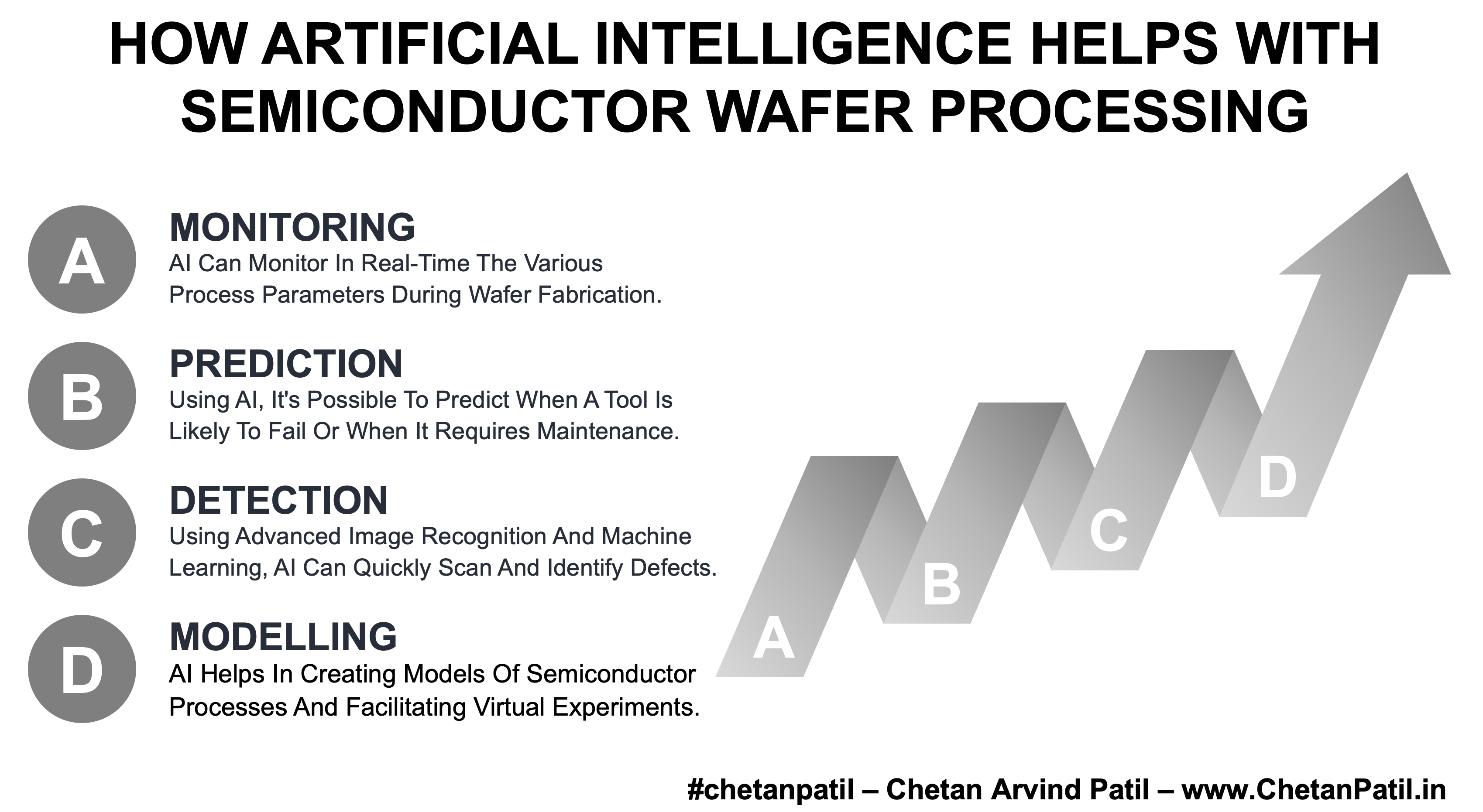
    How LLM AI Agents Can Enhance Semiconductor Production

    In the high-stakes world of semiconductor manufacturing, where precision is paramount and costs are high, LLM AI Agents stand out as a viable and promising solution. Their unique features, such as real-time monitoring, advanced data analytics, and predictive maintenance, offer a distinct advantage. These agents can significantly enhance efficiency, improve quality, and streamline production, making them valuable to any semiconductor production line.

    LLM AI Agents can potentially revolutionize semiconductor production through proactive process optimization. While these agents are already showing promise in various industries, their full impact on semiconductor manufacturing is still emerging.

    The vision is clear: LLM AI Agents could go beyond merely monitoring manufacturing equipment in real-time – they could predict when maintenance might be needed long before any visible issues arise. By leveraging advanced data analytics to detect even the slightest deviations from optimal performance, these agents could help ensure that production lines run smoothly and efficiently, minimizing unplanned downtime and preventing costly disruptions.

    While still being refined and tested, this predictive maintenance concept holds great promise. If fully realized, it could drastically reduce the frequency of unexpected equipment failures, leading to more consistent and reliable production. But the possibilities do not end there. In theory, LLM AI Agents could also dynamically adjust production parameters on the fly, responding to real-time data to optimize processes in previously unimaginable ways.

    For instance, imagine a scenario where a slight change in a deposition process could improve yield. With its advanced analytical capabilities, an LLM AI Agent could identify this opportunity and implement the change immediately, optimizing the process in real time. This would lead to reduced waste, lower costs, and higher throughput – all while maintaining the stringent quality standards that the semiconductor industry demands.

    While these scenarios represent exciting possibilities, it is essential to recognize that they are primarily forward-looking. The full implementation of such capabilities is still on the horizon as researchers and engineers continue to explore and refine how LLM AI Agents can be most effectively integrated into these complex processes.


    Picture By Chetan Arvind Patil

    LLM Potential Use Cases In Semiconductor Manufacturing

    LLM AI Agents could offer various other benefits in semiconductor manufacturing. These include enhancing quality control, optimizing supply chain management, and streamlining design processes. In each of these areas, the advanced capabilities of LLM AI Agents – such as pattern recognition, predictive analytics, and decision-making – could introduce new levels of intelligence and efficiency, paving the way for future innovations.

    Below is an overview of how LLM AI Agents might impact different aspects of semiconductor production if fully realized.

    Use CaseDescriptionBenefits
    Process OptimizationReal-time monitoring and adjustment of manufacturing processes.Reduced downtime, lower costs, higher throughput.
    Quality ControlEarly detection of defects by analyzing production data at various stages.Improved yield, reduced rework, minimized waste.
    Yield EnhancementAnalyzing data to identify factors affecting yield and implementing corrective actions.Higher production yields, increased profitability.
    Test OptimizationAutomating and optimizing test procedures, reducing test times while maintaining accuracy.Faster time-to-market, reduced testing costs.
    Material OptimizationPredicting material performance and optimizing material usage based on historical data.Efficient material use, cost reduction, improved product quality.
    Metrology And InspectionEnhancing metrology techniques by predicting measurement errors and optimizing calibration.Increased accuracy in measurements, reduced inspection times.
    Packaging And AssemblyStreamlining the packaging and assembly processes by optimizing workflows and detecting anomalies.Improved reliability, reduced defects, enhanced assembly efficiency.
    Substrate ManagementMonitoring and optimizing substrate production and handling processes.Improved substrate quality, reduced waste, lower production costs.
    Device ModelingAssisting in device modeling by optimizing simulation parameters and predicting performance issues.Faster design iterations, improved device performance, reduced modeling errors.
    Supply Chain ManagementPredicting bottlenecks, optimizing inventory, and sourcing alternative suppliers.Seamless operations, reduced disruptions, cost savings.

    These use cases illustrate how LLM AI Agents can touch every aspect of semiconductor manufacturing, from the early stages of material selection to the final steps of packaging and assembly.

    By integrating these agents into their operations, manufacturers can unlock new levels of precision, efficiency, and innovation, setting the stage for a future where semiconductor production is more innovative, faster, and more reliable.

    Takeaway: Embracing The Future With LLM AI Agents

    As the demand for smaller, faster, and more efficient semiconductor devices intensifies, LLM AI Agents emerge as a transformative force to meet these challenges. These agents are not just automation tools but intelligent partners that bring new insight and capability to semiconductor manufacturing.

    By integrating LLM AI Agents, semiconductor manufacturers can optimize almost all the stages of semiconductor production, from process control and yield enhancement to supply chain management and device modeling, potentially achieving higher yields, lower costs, reduced waste, and faster time-to-market.

    What truly sets LLM AI Agents apart is their adaptability and continuous learning. Unlike traditional systems, these agents evolve with your processes, constantly improving and adapting to new challenges. This makes them a short-term solution and a long-term strategic asset.

    As the pace of innovation accelerates, those who embrace LLM AI Agents will gain a competitive edge, ensuring they remain at the forefront of the industry. The future of semiconductor manufacturing is not just about keeping up; it’s about leading the way with more innovative, faster, and more efficient operations powered by LLM AI Agents.


  • The Fear Of Using AI For Semiconductor Product Development

    Image Generated Using DALL-E


    AI And Semiconductor

    Integrating Artificial Intelligence (AI) into semiconductor product development is a burgeoning frontier, pushing the limits of what is possible in computation, data processing, and automation. One of the primary fears surrounding the use of AI in semiconductor development is the potential disruption of established processes. The semiconductor industry uses exact, controlled, and standardized manufacturing procedures.

    While the introduction of AI promises enhanced efficiency and innovation, it threatens to upend decades of traditional practices. There is an underlying concern that AI’s learning curve and integration into existing workflows could lead to initial setbacks, inefficiencies, and unforeseen challenges.


    Causes Of Fear

    While introducing AI promises enhanced efficiency and innovation, it threatens to upend decades of traditional practices. There is an underlying concern that AI’s learning curve and integration into existing workflows could lead to initial setbacks, inefficiencies, and unforeseen challenges.

    While AI can optimize and expedite specific tasks, there is also an anxiety about the potential loss of jobs currently integral to the design, testing, and manufacturing processes. Thus, the transition to more AI-driven operations necessitates a workforce skilled in new technologies, raising concerns about the readiness of current employees to adapt and the availability of training opportunities.


    Picture By Chetan Arvind Patil

    AI Leak In Semiconductor

    AI systems require vast amounts of data to learn and make decisions. In semiconductor development, this data can include proprietary designs, manufacturing techniques, and other intellectual properties that are the backbone of competitive advantage.

    Thus, there is a legitimate fear that integrating AI could expose these valuable assets to new risks, including data breaches, espionage, and unauthorized access. Ensuring the security and confidentiality of this information in an AI-enhanced development process poses significant challenges.

    Addressing The Fear Of AI

    Addressing these fears requires a multifaceted approach. Transparency in how AI systems are designed, trained, and implemented can alleviate concerns about reliability and ethics. Robust security protocols are essential to protect intellectual property and sensitive data.

    In addition, regulatory frameworks and industry standards must keep pace with technological advancements, providing a safety net that reassures stakeholders about accountability and ethical considerations.

    By addressing these (and many other not listed) concerns proactively, the semiconductor industry can harness AI’s potential to fuel unprecedented growth and innovation, paving the way for a future where AI and human ingenuity work in concert to push the boundaries of what is possible.


  • The Rise Of Semiconductor Ghiplet

    Image Generated Using DALL-E


    General Purpose GPU

    General Purpose GPUs (GPGPUs) represent a significant evolution in computing, transforming GPUs from specialized hardware focused solely on graphics processing to versatile computing units capable of handling a broad range of tasks. This shift has enabled GPUs to play a crucial role in areas beyond gaming and graphics, including scientific research, data analysis, and artificial intelligence (AI). By leveraging their parallel processing capabilities, GPGPUs can execute complex mathematical and data-intensive operations at speeds vastly superior to traditional CPUs, making them indispensable for tasks requiring high computational throughput.

    Traditionally, GPUs are designed and manufactured as monolithic dies, where a single silicon die houses all the GPU’s functionalities. This approach has advantages, such as straightforward design, manufacturing processes, and high-speed internal communication. However, it also faces limitations in scalability, manufacturing yield, and adaptability to rapidly evolving computational demands, especially those driven by artificial intelligence (AI).


    AI Specific GPU

    As the demand for more versatile and powerful computing resources grows, particularly in AI-driven applications, the semiconductor industry is witnessing the next leap in innovation: the rise of Ghiplet architecture

    Ghiplet technology takes the concept of versatility and scalability to a new level. By adopting a modular approach, where a GPU gets built from multiple interconnected ghiplets, Ghiplet architecture offers unprecedented flexibility in GPU design. This modularity allows for optimizing specific functions, such as AI computations or memory handling, within individual Ghiplets, which can then be customized to meet the unique requirements of various applications.

    Furthermore, the Ghiplet approach addresses some of the critical challenges faced by monolithic designs, such as manufacturing yields and the rapid pace of technological advancement, heralding a new era of GPU technology that is adaptable, efficient, and ready to meet future computing demands.

    Ghiplet = G(PU) + Chiplet


    Flexible And Scalable

    Ghiplet architecture allows for unprecedented flexibility and scalability in GPU design. Depending on an application’s specific needs, different combinations of ghiplets can be assembled to optimize performance, power efficiency, or cost. It starkly contrasts monolithic designs, where changes in functionality or performance often require a complete redesign of the silicon die.

    One of the significant challenges with monolithic dies is the lower yield rates associated with manufacturing large and complex silicon pieces. Defects in any part of the die can render the entire chip unusable, increasing waste and cost. Ghiplet architecture mitigates this issue by using smaller, more manageable ghiplets. Since ghiplets are produced separately, a defect in one ghiplet doesn’t necessitate discarding the entire GPU, significantly improving yield rates and reducing production costs.


    Picture By Chetan Arvind Patil

    Data Movement

    A crucial aspect of making Ghiplet architecture viable is the development of advanced interconnect technologies. These technologies ensure fast, efficient communication between ghiplets, which is essential for maintaining high performance. Innovations such as silicon photonics and advanced packaging solutions, like 2.5D and 3D stacking, are pivotal.

    They enable Ghiplet GPUs to achieve and sometimes surpass, their monolithic counterparts’ communication speeds and bandwidths, overcoming one of the leading technical challenges of modular design.


    AI-GPU For AI-Workload

    AI’s computational demands are a major driving force behind the shift towards Ghiplet architecture. AI applications require massive data processing, often necessitating specialized hardware accelerators. Ghiplet GPUs can integrate AI-specific ghiplets, offering tailored solutions that are more powerful and energy-efficient than monolithic designs can typically provide.

    This adaptability is crucial for staying at the forefront of AI technology development.


    Modular Future

    The Ghiplet concept represents not just a technological innovation but a paradigm shift in how we think about GPU architecture, especially in the context of AI. Understanding the principles and potential of Ghiplet technology is essential for students and future engineers. It offers insights into the future of computing, where flexibility, efficiency, and specialization become critical drivers of semiconductor design.

    As the industry continues to advance, the modular, ghiplet-based approach heralded by Ghiplet technology is set to play a pivotal role in shaping the next generation of computing devices, making it a critical area of study and exploration for anyone interested in cutting-edge semiconductor technology.


  • The Semiconductor AI SoC Company List

    Image Generated Using DALL-E


    The World Of AI SoC

    Artificial Intelligence (AI) has emerged as a cornerstone in the rapidly evolving computing technology landscape, driving innovation across various sectors. At the core of AI’s transformative power are specialized silicon chips, AI Systems on Chips (SoCs), designed to process AI algorithms efficiently. These chips are pivotal in enhancing the performance and capabilities of AI applications, from autonomous vehicles and smart devices to data centers and beyond.

    As AI continues to integrate into our daily lives, the companies behind these advanced SoCs play a critical role in shaping the future of technology. This list introduces the AI SoC companies taking different approaches to designing SoCs for AI applications, spotlighting their contributions to the AI revolution and their impact on the tech industry.


    Picture By Chetan Arvind Patil

    AI SoC Company List

    Below is a work in progress, and if you find AI SoC companies that still need to be listed here, please do reach out to me.

    CompanyDescription
    AmbarellaAI Vision Processors For Edge Applications
    AlphawaveProvides DSP solutions for high-speed, low power consumption, enables building AISoC with AppolloCORE IP, winner of TSMC’s Awards for Excellence.
    Anari AICreating cutting-edge technology to make things work in accordance with the intelligent and scalable future
    Axelera AIRevolutionising the field of artificial intelligence by developing a cutting-edge hardware and software platform for accelerating computer vision on edge devices
    AxiadoTo secure the end-to-end digital infrastructure by embedding a new breed of hardware-anchored AI-driven platform security in servers, 5G and network infrastructure
    BlaizeBlaize has created a transformative new compute solution that unites silicon and software to optimize AI from the edge to the core
    BrainChipSpecializes in developing advanced artificial intelligence and machine learning hardware
    Celestial AICelestial AI is the creator of the Photonic Fabri, an optical interconnect technology platform for compute and memory
    Cambricon TechnologiesFounded in 2016, Cambrian focuses on the research and development and technological innovation of artificial intelligence chip products
    Cerebras SystemsUses Wafer-Scale Engine technology for deep learning, claimed to be 1000 times faster than a GPU, with innovative interconnects, memory, and package technology
    EdgeQFuses Edge and 5G into a single AI-powered chip, aiming to off-load tasks from data centers to Edge Computing
    EnfabricaHardware, software, and system technologies that solve the critical bottlenecks in the next generation AI SoCs
    Esperanto TechnologiesEsperanto delivers high-performance, energy-efficient computing solutions that are the compelling choice for the most demanding AI applications
    EnCharge AILeader in advanced hardware and software systems for AI computing
    Flex LogicDeveloper of embed field-programmable gate IP focused on AI SoC
    GrAI Matter LabsCreated the fastest edge AI processor for machine vision in robotics, AR/VR, drones and more
    GraphcoreHas built a new type of processor for machine intelligence to accelerate machine learning and AI applications for a world of intelligent machines
    GroqLeverages Tensor Streaming Processor (TPU) for high-speed memory and fast operations, packed in a tiny package
    HailoFocuses on Edge AI, claims its Hailo processor can deliver better TOPS with high area and power efficiency
    Horizon RoboticsDesigned AI-enabled Brain Processing Units (BPU) for the automotive (Journey BPU) and IoT (Sunrise BPU) markets
    HabanaCreates world-class AI Processors, developed from the ground-up and optimized for training deep neural networks and for inference deployment in production environments
    KneronDevelops an application-specific integrated circuit and software that offers artificial intelligence-based tools
    KinaraKinara processors drive AI applications demanding low latency, high performance, and low power
    LeapMindFocuses on edge AI and machine learning
    LightelligenceProviding customers with powerful and effective computing power through a new paradigm of optoelectronic computing
    LightmatterChip architecture, powering faster, energy-efficient computing with photonic processors for sustainable AI advancement
    Luminous ComputingLeverages photonics for faster AI workload training, still in stealth mode
    Mythic AIUtilizes Intelligence Processing Units (IPUs) for efficient, performance-oriented, cost-efficient AISoC, offers Mythic Analog Matrix Processor
    NeurealityDeveloping AI inferencing accelerator chips
    PropheseeUses a patented sensor design and AI algorithms that mimic the eye and brain to reveal what was invisible until now using standard frame-based technology
    RebellionsDevelops AI accelerators by bridging the gap between underlying silicon architectures and deep learning algorithms
    Rain NeuromorphicsBuilding the most energy efficient hardware for AI
    SambaNova SystemsAI hardware and integrated systems to run AI applications from the data center to the cloud
    SiMa.aiAims for greener, low-power AISoC for Edge AI, details forthcoming, plans new silicon launch
    Synthara AGEnables seamless integration of in-memory computing capabilities to existing chip designs, making them 130 times faster and 150 times for energy efficient
    SyntiantLeader in edge-AI deployments, bringing deep-learning to any device with industry-leading Neural Decision Processors and hardware-agnostic machine learning models
    TenstorrentNext-generation computing company that utilizes RISC-V that builds computers for AI
    Wave ComputingAccelerates AI computing with MIPS architecture, offers M-Class product for IoT and smart devices

    Why Care About AI SoC Companies

    Understanding and keeping track of AI Systems-On-A-Chip (SoC) companies is crucial for several reasons. Firstly, these companies are at the forefront of developing the foundational technology that powers various AI applications, from consumer electronics to critical infrastructure.

    Their innovations in chip design and processing capabilities directly influence the efficiency, performance, and powers of AI systems, affecting everything from energy consumption to processing speed and accuracy.

    Furthermore, as AI becomes more integrated into our daily lives, these companies’ strategies and market positions have significant economic and technological implications.

    By understanding the landscape of AI SoC companies, stakeholders can better navigate the technological shifts, investment opportunities, and policy considerations that shape our digital future.


  • The AI Centers And Implications On Semiconductor Industry

    Image Generated Using DALL-E


    Data To AI Centers

    Data centers have been essential for storing, managing, and processing data for several decades. However, we are now on the brink of a new era of technology, and a significant shift is imminent. Traditional data centers will be replaced by AI Centers, a new technology hub specifically designed to cater to the growing demands of Artificial Narrow Intelligence (ANI), Artificial General Intelligence (AGI), and Artificial Super Intelligence (ASI).

    AI Centers: AI Centers Will Get Equipped With The Best XPUs In The Market. It Will Drive The Need To Push Everything Toward AGI And Then ASI. Eventually, It Will Also Lead To The Creation Of AI Centers Cum AI FABs That Will Then Turn Into AI RnD Center And So On.

    AI Centers, as the term suggests, are dedicated facilities equipped with advanced computational resources, primarily for ANI, AGI, and ASI. Unlike conventional data centers that handle a broad spectrum of data-related tasks, AI Centers will be optimized for the intensive computational demands of AI algorithms.

    The shift towards AI Centers is propelled mainly by the increasing integration of AI features in software solutions across various industries. AI’s capabilities in pattern recognition, predictive analytics, generative AI, and similar automation are becoming indispensable in almost all industries. This widespread adoption necessitates infrastructure that can efficiently handle the unique computational requirements of AI, which is where AI Centers come into the picture.


    Picture By Chetan Arvind Patil

    How AI Centers Differ From Data Centers

    To understand more about AI Centers. First, we look at how Data Centers differ from AI Centers. The only significant difference between them is the processing power that AI Centers demand. Which eventually needs more specialized processors. At the same time, the energy demand of AI centers is ten times that of data centers. AI Centers will cost more to set up and run in the long run.

    However, the benefits of such a center will outweigh the negatives. For example, quickly computing (based on historical data) and predicting the right medical treatments could save doctors a lot of time. Eventually, this leads to sound decisions. It could also be a game changer in research areas like cancers and other severe medical conditions.

    ASPECTDATA CENTERSAI CENTERS
    Primary FunctionStorage and management of large data setsFocused on AI and ML computations
    Processing PowerHigh, but generalizedExtremely high, specialized for AI tasks
    HardwareStandard CPUs and storage devicesAdvanced XPUs, GPUs, TPUs, ASICs
    SoftwareGeneral-purpose operating systems and appsSpecialized AI and ML algorithms
    Data ProcessingBroad spectrum, including transactional dataPrimarily for AI model training and inference
    Energy ConsumptionHigh, but less specializedExtremely high, due to intensive computations
    Cooling RequirementsSignificant, due to dense hardwareEven higher, due to more intense processing
    Storage CapacityMassive, for diverse data typesOptimized for fast access rather than volume
    Network InfrastructureRobust, for varied trafficUltra-high-speed, for rapid data processing
    ScalabilityDesigned for incremental growthRequires scaling specialized hardware
    Security ConcernsHigh, due to diverse data storageHigh, with added focus on model integrity
    Cost of Setup and OperationHigh, but standardizedHigher, due to specialized equipment
    Maintenance ComplexityModerateHigh, due to specialized hardware and software
    Business ModelService-oriented (e.g., cloud storage)Driven by AI-as-a-Service offerings
    Market DemandConsistent, for various IT needsGrowing rapidly, driven by AI advancements
    Innovation PaceSteady, with gradual improvementsRapid, aligned with AI and ML breakthroughs
    Workforce SkillsIT and data management focusedAI, ML, and specialized hardware expertise
    Environmental ImpactSignificant, due to energy usePotentially higher, depending on efficiency gains
    Regulatory ComplianceData privacy and security lawsAdditional concerns with AI ethics and transparency
    Future OutlookEssential but evolving towards integration with AICentral to the advancement of AI and its applications

    Impact On Semiconductor Industry

    The heart of these AI Centers will be the XPUs – a broad term encompassing a range of specialized processing units like GPUs (Graphics Processing Units), TPUs (Tensor Processing Units), and other Application-Specific Integrated Circuits (ASICs). These processors are designed to handle the parallel processing tasks that AI and ML algorithms demand.

    The semiconductor industry will need to innovate continuously to keep up with the evolving requirements of AI algorithms. It could mean designing more powerful and efficient chips and custom hardware solutions tailored for specific AI applications.

    The development of AI Centers will likely lead to increased investment in the semiconductor industry in terms of capital and research. Collaborations between tech companies and semiconductor manufacturers could become more common as they work together to optimize hardware for AI applications.

    While this shift presents lucrative opportunities for the semiconductor industry, it also brings challenges. Scaling production, managing power consumption, and ensuring the sustainability of materials are some of the hurdles that must be addressed.

    Take Away

    The transition from traditional data centers to AI Centers marks a significant turning point in the computing and semiconductor industries. As AI continues incorporating its way into various software solutions, the demand for specialized, high-performance computing resources will surge. It presents unique challenges and opportunities for the semiconductor industry, driving innovation and collaboration in new and exciting ways.


  • The Quick Guide On Semiconductor Powered AI Accelerator

    Image Generated Using DALL-E


    An AI Accelerator is specialized hardware designed to process artificial intelligence (AI) tasks efficiently. These accelerators are specifically optimized to handle computations related to machine learning and deep learning algorithms, which are the core of most modern AI applications.

    Key features and purposes of AI Accelerators include:

    Efficiency: Designed to be more efficient than general-purpose processors like CPUs (Central Processing Units) for AI tasks. This efficiency comes from faster processing times due to higher throughput via multiple processing elements.

    Parallel Processing: AI algorithms benefit from similar processing capabilities, especially those in neural networks. AI accelerators often have architectures that support high degrees of parallelism, allowing them to process multiple operations simultaneously.

    Optimized Operations: AI accelerators get optimized for the types of mathematical operations most common in AI workloads, such as matrix multiplication and vector operations, which are crucial for neural network computations.

    Memory Bandwidth: High memory bandwidth is essential for AI workloads, and these accelerators often have specialized memory architectures to support fast data access.

    Scalability: AI accelerators can be scaled to support larger models and datasets, which is vital as the complexity of AI tasks continues to grow.

    These features make AI accelerators indispensable in various applications, ranging from natural language processing and image recognition to autonomous vehicles and advanced analytics, driving innovation and efficiency in AI development and deployment.


    Picture By Chetan Arvind Patil

    AI accelerators, despite their numerous advantages in enhancing the performance of AI and machine learning tasks, also come with certain drawbacks:

    High Cost: AI accelerators, especially the more advanced models, can be expensive. This high cost can be a barrier for smaller companies and startups needing more money for such investments.

    Specialized Hardware Requirements: Since these accelerators are specialized hardware, integrating them into existing systems can sometimes be challenging. They may require specific motherboards, power supplies, and cooling systems, which adds to the complexity and cost.

    Limited Flexibility: Some AI accelerators, particularly ASICs like TPUs, are highly optimized for specific tasks or computations. This specialization can limit their flexibility, making them less suitable for a broader range of applications or emerging AI algorithms requiring different computational capabilities.

    Software Ecosystem And Compatibility: AI accelerators rely heavily on software and frameworks compatible with their architecture. This dependency means that changes or updates in software could necessitate adjustments in the hardware or vice versa, potentially leading to compatibility issues.

    Complexity In Programming And Maintenance: Programming AI accelerators requires specialized knowledge and skills, particularly for optimizing the performance of AI models. Additionally, maintaining these systems, both in terms of software and hardware, can be complex and resource-intensive.

    Power Consumption And Heat Generation: High-performance AI accelerators can consume significant power and generate considerable heat, especially in large data centers. It necessitates sophisticated cooling solutions and can lead to higher operational costs.

    Scalability Challenges: While AI accelerators are scalable, scaling them to extensive systems can be challenging and expensive, especially in data center environments where thousands of accelerators might be required, leading to increased complexity in infrastructure, power, and cooling requirements.

    Rapid Obsolescence: AI and machine learning are advancing rapidly, and hardware can quickly become obsolete as more new models emerge. This fast pace of development can make it challenging for organizations to keep up with the latest technology without significant ongoing investment.

    In conclusion, AI accelerators significantly advance artificial intelligence and machine learning, offering unparalleled efficiency and performance for complex computational tasks. These specialized hardware components have become crucial in powering a wide range of AI applications, from deep learning models in data centers to real-time processing in edge devices.

    While they offer substantial benefits regarding processing speed and energy efficiency, challenges, such as high cost, specialized hardware requirements, limited flexibility, and rapid obsolescence, must be carefully considered. As the AI landscape continues to evolve rapidly, AI accelerators stand as a testament to the ongoing synergy between hardware innovation and software development, driving forward the capabilities and applications of AI technology in an increasingly digital world.


  • The Ways In Which OpenAI Can Reinvent Semiconductor Chip Development

    Image Generated Using DALL-E


    OpenAI’s involvement in semiconductor chip development could mark a significant shift in the industry, bringing about advancements in silicon design, silicon software stack development, R&D investment, and the application of GenAI in chip design.

    However, the complexity and cost of chip development have escalated, posing significant challenges. It is where OpenAI, with its cutting-edge AI technologies, can play a transformative role.

    Let’s explore how OpenAI can revolutionize the various aspects of semiconductor chip development.

    Empowering Chip Development Teams With AI:

    The first area where OpenAI can make a substantial impact is in augmenting the capabilities of chip development teams. AI models, especially those developed by OpenAI, can analyze vast amounts of data from previous chip designs, manufacturing processes, and performance metrics.

    This analysis can lead to insights that would only be possible for human teams to discern due to the sheer volume and complexity of the data.

    For instance, AI can predict how minor changes in the design might affect the chip’s overall performance and energy efficiency. This predictive capability can significantly reduce the time and cost of trial-and-error methods traditionally used in chip design.

    Revolutionizing The Software Stack For Chip Design:

    The software stack used in chip design, from schematic capture to physical layout, is ripe for innovation. OpenAI’s models can be integrated into these software tools to enhance functionality.

    For example, AI can automate parts of the layout process, optimizing the placement of components to minimize signal delays and power consumption while maximizing performance.

    Moreover, AI can assist in the verification process, quickly identifying potential errors or inefficiencies in the design. This integration can drastically reduce the time to market for new chips and improve their overall quality and performance.


    Picture By Chetan Arvind Patil

    Investing In R&D And Knowledge Building:

    OpenAI’s involvement in semiconductor chip development is not just about directly applying AI technologies by building AI silicon chips but also about fostering a deeper understanding of the field.

    By investing in research and development, OpenAI can help uncover new design methodologies and manufacturing techniques that could revolutionize the industry.

    Furthermore, OpenAI can contribute to knowledge building around silicon chip design and manufacturing. It could involve developing AI models that simulate different manufacturing processes or predict the performance of new materials, thereby providing valuable insights to researchers and engineers.

    GenAI For Silicon Chip Design:

    The most futuristic application of OpenAI in chip development is the concept of Generative AI (GenAI) for silicon chip design. GenAI can go beyond optimization and generate novel chip designs based on specified parameters and performance goals.

    This approach could lead to breakthroughs in chip design, uncovering configurations and architectures that humans might not conceive.

    For instance, GenAI could design chips optimized explicitly for AI workloads or ultra-efficient chips for use in smart devices. The potential here is vast, and as AI technology continues to evolve, so will its chip design capabilities.

    Integrating OpenAI’s technologies into semiconductor chip development heralds a new era of innovation and efficiency.

    By empowering development teams, revolutionizing the silicon software stack, investing in R&D, and leveraging GenAI, OpenAI can help overcome current limitations and open up new possibilities in chip design and manufacturing.

    As these technologies mature, we can expect faster, more efficient, and more powerful semiconductor chips, driving the next wave of technological advancement.


  • The AI World Beyond Semiconductor GPUs

    Image Generated Using Adobe Firefly


    Graphics Processor Units (GPUs) have become the default go-to architecture whenever the requirement is for faster throughput. The primary reason is the massively parallel processing with the help of many cores and how the memories get organized around them.

    Due to the benefits of such an architecture, the AI World has also adopted GPUs as its go-to silicon architecture. The goal is to process large amounts of data in the shortest time possible; other technical reasons are reusability and portability, which lower the entry barrier for new companies developing large-scale AI solutions.

    Several semiconductor companies provide GPU solutions. However, NVIDIA is winning the GPU race so far, and the main reason is the near-perfect software-to-silicon ecosystem it has created. It enables new and existing customers to adapt to the latest GPU type swiftly and also new AI Frameworks, all while keeping the reusability and portability cost under check.

    What does not work in favor of GPU architecture:

    Availability: GPUs (mainly from NVIDIA) are inching towards 3nm. There will be a race to capture the available worldwide capacity with only one Pure-Play vendor capable of producing yieldable silicon chips. It will take a lot of work to capture the required demand-drive power.

    Cost: GPU will start adopting ultra-advanced (3nm and lower) nodes. The cost of designing and manufacturing these silicon chips will increase further. More so when GPUs are yet to find a way out of the die-level solution to a more More-Than-Moore (MtM) path. In a year or two, GPUs designed for AI workload will surely reach the reticle limit, which even EUVs cannot support.

    Not Application-Specific: GPUs are still general-purpose in terms of application requirements. The SIMD, MIMD, Floating, and Vector level translations usually only fit some requirements. Conversely, the AI developers (mainly large-scale software companies) will keep seeing the need for more application-specific (thus why TPUs came into existence) architecture that can provide a solution-level GPU.

    Deployment: Deploying stacked GPUs is like bringing up a massive farm. It increases the cost of operating such data farms. On top of that, the more powerful the GPUs are, the more influential the applications become. Thus, increasing the data processing request leads to more performance and energy consumption.

    Sooner or later, even GPU architecture will reach a state where they may not be the first choice for AI. Currently, the software industry (or the AI industry) relies on the GPU architecture primarily due to the mega data centers using these and being the best broadly deployed architecture in the market.

    However, as more new types of AI usage and requirements arise, the software industry will realize that the GPU architecture is unsuitable for their applications. Thus, there is a demand for more customized performance-oriented silicon architecture.


    Picture By Chetan Arvind Patil

    The need for customized AI silicon architecture has already caught the eyes of both the software and silicon industry. It is leading to more silicon-level solutions. That can replace or give GPU architecture robust competition.

    There is a specific type of silicon architecture that has the potential to replace GPUs shortly. Below are a few:

    Wafer-Scale Engine (WSE) SoCs:

    The Wafer-Scale Engine (WSE) represents a paradigm shift in computing, indicating a new era where traditional GPUs get replaced in specific applications. Unlike GPUs that contain thousands of small processors, a WSE is a single, giant chip that can house hundreds of thousands of cores capable of parallel processing. This architectural leap enables a WSE to process AI and machine learning workloads more efficiently due to its vast on-chip memory and reduced data transfer latency. By eliminating the bottlenecks inherent in multi-chip approaches, a WSE can deliver unprecedented performance, potentially outpacing GPUs in tasks that can leverage its massive, monolithic design. As AI and complex simulations demand ever-faster computational speeds, WSEs could supplant GPUs in high-performance computing tasks, offering a glimpse into the future of specialized computing hardware.

    Chiplets With RISC-V SoCs:

    Chiplets utilizing the RISC-V architecture present a compelling alternative to conventional GPUs for specific computing tasks, mainly due to their modularity and customizability. RISC-V, being an open-source instruction set architecture (ISA), allows for the creation of specialized processing units tailored to specific workloads. When these processors adopt chiplets (small, modular silicon blocks), the larger chip can be manufactured into a coherent, scalable system. The computing system gets optimized for parallel processing, similar to GPUs, but with the added advantage of each chiplet being custom-crafted to handle particular segments of a workload efficiently. In scenarios where energy efficiency, space constraints, and specific application optimizations are paramount, RISC-V chiplets could feasibly replace GPUs by providing similar or superior performance metrics while reducing power consumption and increasing processing speed by tailoring the hardware directly to the software’s needs.

    Tensor Processing Units SoCs:

    Tensor Processing Units (TPUs), application-specific integrated circuits (ASICs) designed for machine learning tasks, offer a specialized alternative to GPUs. As System-on-a-chip (SoC) designs, TPUs integrate all the components needed for neural network processing onto a single chip, including memory and high-speed interconnects. Their architecture is tuned for the rapid execution of tensor operations, the heart of many AI algorithms, which enables them to process these workloads more efficiently than the more general-purpose GPUs. With their ability to perform a higher number of operations per watt and their lower latency due to on-chip integration, TPUs in an SoC format can provide a more efficient solution for companies running large-scale machine learning computations, potentially replacing GPUs in data centers and AI research facilities where the speed and efficiency of neural network processing are crucial.

    PIM SoCs:

    Processing-in-memory (PIM) technology, particularly when embedded within a System on a Chip (SoC), is poised to disrupt the traditional GPU market by addressing the ‘memory wall’ problem. PIM architectures integrate processing capabilities directly into the memory chips, allowing data computation where it is stored, thereby reducing the time and energy spent moving data between the processor and memory. As an SoC, integrating PIM with other necessary system components can lead to even more significant optimizations and system-level efficiency. In applications such as data analytics, neural networks, and other tasks that require rapid, parallel processing of large data sets, PIM SoCs could potentially outperform GPUs by leveraging their ability to bypass the data transfer bottlenecks that GPUs face, delivering faster insights and responses, especially in real-time processing scenarios.

    One factor all of the above solutions need to success is the software ecosystem that AI developers can rely on. All new solutions do require a level of abstraction that can make it easier to adopt. So far, with the CUDA ecosystem and optimized AI frameworks around CUDA, NVIDIA has aced this domain.

    Like the CPU domain, the GPU domain cannot be dominated by a selected few. Soon, there will be promising SoCs that can pitch themselves as the potential future of the AI World, which will also push GPU architecture innovation to its limit.

    The next five years will reveal how the “Silicon Chip For AI World” segment will evolve, but it certainly is poised for disruption.


  • The Semiconductor AISoC Platform Alliance

    The Semiconductor AISoC Platform Alliance

    Image Generated Using Adobe Firefly


    The realm of artificial intelligence (AI) is experiencing a transformative shift, primarily driven by innovative AI chips developed by startups. These enterprises are challenging the status quo, bringing cutting-edge chip architectures tailored to optimize deep learning, neural networks, and other AI tasks.

    By pushing the boundaries of processing speed, energy efficiency, and on-chip intelligence, these startups are enhancing AI’s capabilities and making it more accessible.

    To take this to a new level, early this week, several leading AI chip startups, including Ampere, Cerebras Systems, Furiosa, Graphcore, and others, announced a consortium called the AI Platform Alliance. Spearheaded by Ampere, this alliance seeks to make AI platforms more open, efficient, and sustainable.

    Image Source: AI Platform Alliance

    As the AI Platform Alliance progresses further, there will be more startups that will join the alliance. In the long run, bringing more silicon chip ideas forward will be an excellent initiative. Also, some of the critical areas where this AI Platform Alliance can be crucial:

    Software: Making it more accessible for emerging AI silicon startups to create silicon chips by quickly enabling the porting of existing applications. Something which several of the AI chip startups struggle with.

    Open Source: Enabling more open-source AI silicon chip initiatives that could make it easier for future startups to bring their products to market quickly.

    Standards: By providing more standardized AI chip-focused protocols to lower the new startups’ technology barrier.

    Benchmarking: Coming up with more standardized AI-focused benchmarking that can bring reliable comparison across silicon architectures.


    Picture By Chetan Arvind Patil

    Let us also look at the companies/startups developing silicon-level technology to drive AISoC design, which also leads the efforts to launch the AI Platform Alliance.

    Ampere Computing: Ampere Computing is a company known for designing and developing cloud-native Arm-based processors, primarily targeting data centers and cloud computing environments. The company utilizes the Arm architecture for its processors.

    Cerebras Systems: Cerebras Systems is a pioneering technology company known for its groundbreaking work in artificial intelligence (AI) hardware. Their flagship product, the Cerebras Wafer Scale Engine (WSE), stands out as the world’s most significant semiconductor device, encompassing an entire silicon wafer. Unlike traditional chip manufacturing, where individual chips are from a silicon wafer, the WSE utilizes the whole wafer, resulting in a single, massive chip with over 1.2 trillion transistors and 400,000 AI-optimized cores. Cerebras aims to accelerate deep learning tasks and push the boundaries of AI computational capabilities.

    FurisoaAI: FuriosaAI is an AI chip startup company that creates next-generation NPU products to help you unlock the next frontier of AI deployment. Next year, FurisoAI is gearing up to launch a High Bandwidth Memory 3 (HBM3) powered silicon chip that can provide H100-level performance to power Chat-GPT-scale models.

    Graphcore: Graphcore is a notable artificial intelligence (AI) hardware player. Established in 2016 and headquartered in Bristol, UK, the company has made significant strides in developing specialized processors for machine learning and AI applications. Their primary product is the Intelligence Processing Unit (IPU), a novel chip architecture designed from the ground up to accelerate both training and inference tasks in deep learning.

    Kalray: Not a startup. Kalray is a technology company specializing in designing and developing multi-core processors for embedded and data center applications. Founded in 2008 and headquartered in Grenoble, France, Kalray’s primary offering is the MPPA (Massively Parallel Processor Array) technology. This unique processor architecture is designed to provide a high level of computing power while maintaining energy efficiency, making it suitable for applications where both performance and low power consumption are crucial.

    Kinara: Led by Silicon Valley veterans and a development team in India, Kinara focuses on Edge AI processors and modules that deliver scalable performance options to support applications with stringent power demands or the highest computing requirements. It has launched Ara-1, an edge AI Processor to provide the ideal balance of computing performance and power efficiency to optimize intelligent applications at the border.

    Luminous Computing: In the early stage of silicon chip development. Luminous is focusing on building the most powerful, scalable AI accelerator.

    Neuchips: Neuchips is an AI ASIC solution focusing on signal processing, neural networks, and circuit design. It also has a good portfolio of products that range from highly accurate AI computing engines to efficient recommendation inference engines.

    Rebellions: Focused on bringing the world’s best inference performance for Edge and Cloud Computing. Their ATOM series delivers uncompromised inference performance across different ML tasks, computer vision, natural language processing, and recommendation models.

    SAPEON: Focused on building a Hyper-Cloud AI Processor. SAPEON has an optimal architecture for low-latency, large-scale inference of deep neural networks. They have already launched products designed to process artificial intelligence tasks faster, using less power by efficiently processing large amounts of data simultaneously.

    Given the surge in AI’s popularity, there’s an increasing demand for computing power, with AI inferencing needing up to 10 times more computing over its lifespan. Such an alliance can help improve power and cost efficiency in AI hardware to surpass GPU performance levels.

    AI Platform Alliance plans to create community-developed AI solutions, emphasizing openness, efficiency, and responsible, sustainable infrastructure. It is undoubtedly a significant step towards creating a new class of AISoCs.


  • How Artificial Intelligence Helps With Semiconductor Wafer Processing

    How Artificial Intelligence Helps With Semiconductor Wafer Processing

    Image Generated Using Adobe Firefly


    Semiconductor wafer processing is an intricate series of steps to produce integrated circuits on silicon wafers. Artificial Intelligence (AI) has proven to be a powerful tool in refining and enhancing these processes.

    AI offers a range of applications in semiconductor wafer processing. Leveraging AI technologies can significantly improve efficiency, yield, and quality. Below are some of the key ways in which AI assists in semiconductor wafer processing:

    Process Monitoring:

    AI can monitor in real-time the various process parameters during wafer fabrication. AI can predict potential issues by analyzing this data and making real-time adjustments to maintain optimal conditions, ensuring consistent quality across wafers and batches.

    Predictive Maintenance:

    Tools and machines used in wafer processing need regular maintenance. Using AI and machine learning algorithms, predicting when a tool/machine will likely fail or require maintenance is possible. It reduces unplanned downtime and ensures maximum uptime, which is crucial for high-volume manufacturing environments.

    Defect Detection:

    Inspecting wafers for defects is a critical step. Using advanced image recognition and machine learning, AI can quickly scan and identify weaknesses that might be hard for a human to detect. Early defect detection can lead to process improvements and reduced wastage.

    Process Optimization:

    By collecting and analyzing vast amounts of data from various process steps, AI can help optimize process parameters. It not only increases yield but also improves the overall efficiency of the wafer production line.

    Besides optimizing processes and detecting issues with the silicon wafer, AI solutions are also being deployed to model and predict future scenarios.


    Picture By Chetan Arvind Patil

    By utilizing prediction techniques, the wafer process is more data-driven and can enable optimized flow that can help in increasing the wafer processed per hour.

    Modeling:

    AI can help create accurate models of semiconductor processes, facilitating virtual experiments. It aids in understanding potential outcomes without actually running expensive real-world experiments.

    Yield Prediction:

    By analyzing historical data and real-time inputs, AI models can predict the yield of a particular batch of wafers. It helps make informed decisions regarding resource allocation, process adjustments, and inventory management.

    Optimal Utilization:

    AI can guide the optimal use of gases, chemicals, and other resources in the wafer processing pipeline, ensuring minimal waste and cost efficiency.

    Data Analysis:

    Semiconductor processing generates vast amounts of data. AI can analyze this data faster and more accurately than traditional methods, extracting valuable insights that can lead to process improvements.

    Integrating AI into semiconductor wafer processing has proved to be an efficient and cost-effective way to ensure high-quality products with a better yield.

    As AI technologies evolve and become even more sophisticated, their role in the semiconductor industry will expand, resulting in further innovations.