Category: BLOG

  • The Semiconductor Major Selection Guide For Undergraduate In India

    Image Generated Using DALL-E


    India And Semiconductor Talent

    I have been getting a lot of emails and messages (on social media) regarding how a student (mainly in India) can wisely decide which specific undergraduate engineering majors to select to ensure the coursework-based training aligns with the semiconductor industry’s requirements. Thus, it also offers a better career perspective, more so when there are so many engineering majors to opt for, and therefore needs more explicit guidance on how and when one of many bridges the path towards a career as a semiconductor engineer.

    Such a knowledge gap becomes more concerning for a country like India, which has a solid ambition for digitalization and the government’s push towards making India a hub for electronic manufacturing. And to succeed in this, skilled students in India will play a vital role.

    To bridge this knowledge gap of undergraduate major vs semiconductor engineering, in the subsequent part of this blog, I will emphasize the following points:

    • Levels Of Education That Lead To A Career In Semiconductor Industry
    • Semiconductor Engineering Majors Versus Semiconductor Industry
    • Engineering Degree Versus Semiconductor Industry Requirements

    For the sake of simplicity, I will exclude the details of how the entrance examination process in India works. To simplify, let us assume any student with an interest in semiconductor engineering has the option to select an undergraduate major that can correctly set the roadmap for a semiconductor career.


    Levels Of Education That Lead To A Career In Semiconductor Industry

    I have observed that the journey to a career in the semiconductor industry can be embarked upon at various educational levels, each leading to distinct knowledge bases and career trajectories. These levels range from Diplomas to Ph.D. programs, and each plays a critical role in shaping an individual’s professional path in this dynamic field.

    Diplomas offer a practical and focused introduction to electronics, mechanics, and other relevant fields. A certificate can be a stepping stone for individuals looking to enter the industry quickly, providing essential technical skills and a foundational understanding of semiconductor technology. Typically, diploma holders begin their careers in technician roles, overseeing aspects of semiconductor manufacturing or, at the max, basic design. As I have seen, these roles, while more hands-on and less theoretical, are crucial for the day-to-day operations of the semiconductor industry. In the long term, the growth opportunities are limited.

    Bachelor’s degrees, such as a B.Tech or B.E., delve deeper into the theoretical and practical aspects of engineering disciplines related to semiconductors, like Electronics and Communication, Electrical Engineering, or Materials Science. With a bachelor’s degree, individuals have a comprehensive understanding of the principles and applications of semiconductor technology. Graduates often find design, development, and innovation opportunities, taking on roles that involve more responsibility and creative input than diploma holders. They are instrumental in driving the industry forward through engineering and design innovations.

    Moving to higher education, Master’s and Ph.D. programs offer specialized knowledge and research opportunities. A Master’s degree allows specialization in niche areas within the semiconductor field, such as VLSI design, nanotechnology, or semiconductor materials. This level of education often leads to more advanced positions in industry research and development or management roles. 

    A Ph.D., the pinnacle of academic achievement, involves deep research and contributes to groundbreaking advancements in semiconductor technologies. Ph.D. holders typically engage in cutting-edge research, academics, or high-level industry innovation and decision-making. They are the trailblazers, pushing the boundaries of what’s possible in semiconductor technology.

    In my ten years of academia and industry experience, each educational level caters to different aspects of the semiconductor industry, from operational roles to innovation and leadership.

    Whether through hands-on skills acquired in diploma programs or the advanced research capabilities honed during a Ph.D., every level of education plays a vital role in the growth and advancement of this ever-evolving field.


    Picture By Chetan Arvind Patil

    Semiconductor Engineering Majors Versus Semiconductor Industry Engineering Majors

    Beneath, I have summarized almost all major engineering disciplines directly related to semiconductor engineering. At least in India, the more specialized degree programs have yet to be offered. However, the guide below is handy for students who need to learn how the major they select will impact if they wish to opt for a career in the semiconductor industry.

    Another critical point to note is that selecting an undergraduate degree also has a say on which master’s and research degree one will pursue. I hope this table helps students both from an education and also a career point of view.

    MajorDescriptionKey SubjectsCareer Prospects In Semiconductor Industry
    Electronics and Communication Engineering (ECE)Focuses on electronic circuits, communication systems, and related technologies. Directly aligned with semiconductor industry.– Digital and Analog Electronics
    – Microprocessors and Microcontrollers
    – Signal Processing
    – Communication Systems
    – VLSI Design
    – Chip Design and Manufacturing
    – Communication Systems Development
    – Quality Control and Testing
    – Research and Development
    Electrical Engineering (EE) And/Or Electronics Engineering (EE)Covers a broad range of topics related to power electronics, and electromagnetism, crucial for semiconductor devices. In many countries, ECE is often termed as EE.– Circuit Analysis
    – Control Systems
    – Power Electronics
    – Electrical Machines
    – Electromagnetic Theory
    – Semiconductor Manufacturing and Process Engineering
    – Chip Design And Manufacturing
    – Design and Maintenance of Power Systems in Plants
    – Equipment and Tool Development
    Material Science and EngineeringStudy of materials used in semiconductor manufacturing. Focus on properties, performance, and processing of materials.– Thermodynamics of Materials
    – Physical Metallurgy
    – Polymer Science
    – Ceramics
    – Nanomaterials
    – Material Research and Development
    – Quality Analysis in Manufacturing
    – Process Development for New Materials
    Computer EngineeringCombines electrical engineering and computer science, focusing on computer systems and software for semiconductor design.– Computer Architecture
    – Operating Systems
    – Algorithm Design
    – Embedded Systems
    – Digital System Design
    – Software Development for Semiconductor Devices
    – Embedded Systems
    – Chip Design and Testing
    – System Integration
    – Product Engineering
    NanotechnologyDeals with structures and devices at the atomic and molecular scale, enabling advancements in semiconductor technology.– Nanochemistry
    – Quantum Mechanics
    – Nanofabrication
    – Nano-scale Electronics
    – Molecular Engineering
    – R&D in Advanced Technologies
    – Nanoscale Manufacturing Processes
    – Innovation in Fabrication Techniques
    – Quality Control and Testing at Nanoscale
    Mechanical Engineering (With Focus On Microelectronics)Application of mechanical principles to the design and manufacture of microelectronic systems in semiconductor devices.– Mechanics of Materials
    – Thermodynamics
    – Microfabrication Technology
    – Fluid Mechanics
    – Heat Transfer
    – Design and Manufacturing of Equipment
    – Thermal Management in Devices
    – Microelectronic Packaging and Reliability Analysis
    – Process Engineering in Fabrication
    Chemical Engineering (With Focus on Semiconductor Processing)Focuses on chemical processes and materials in semiconductor manufacturing, crucial for fabrication processes.– Chemical Process Principles
    – Semiconductor Materials and Processes
    – Surface and Colloid Chemistry
    – Nanotechnology in Chemistry
    – Fabrication and Processing
    – Material Development for Devices
    – Quality Control in Chemical Processes
    – R&D in Semiconductor Materials
    Photonics EngineeringCentered around the use of light in technology, highly relevant to optoelectronics and fiber optics in semiconductors.– Optics and Lasers
    – Optical Fiber Technology
    – Photonic Devices and Systems
    – Quantum Electronics
    – Development of Optoelectronic Devices
    – Fiber Optics Communication System Design
    – Research in Photonic-based Technologies
    – Quality Testing and Control in Applications
    Industrial EngineeringFocuses on optimizing complex processes and systems, crucial for improving efficiency and productivity in semiconductor manufacturing.– Operations Research
    – Systems Engineering
    – Production Planning and Control
    – Quality Control
    – Supply Chain Management
    – Process Optimization in Semiconductor Manufacturing
    – Supply Chain Management for Semiconductor Products
    – Quality Assurance and Control
    – Production Planning and Management
    – Systems Analysis and Design


    Source: SRC MAPT

    Engineering Degree Versus Semiconductor Industry Requirements

    To correlate the engineering majors with the semiconductor industry’s requirements, a student will find it easier to decipher SRC’s Knowledge, Skills, And Abilities (KSA) chart.

    The KSA matrix was developed based on the inputs from experts across the semiconductor industry. The content of the KSA Matrix should adapt to the dynamic changes in the landscape of semiconductor talent requirements.

    StepDescription
    Identify Core Skills For Desired RolesStudents should examine the matrix to identify critical or desired skills for roles they are interested in. For example, skills under ‘Device & Circuit Concepts’, ‘System Design, Verification, Validation & Simulation Tools’ are key for a design role.
    Map Majors To SkillsMap the core subjects of the major to the skills listed in the matrix. An ECE major aligns their circuit design and signal processing knowledge with skills required for roles like Analog Design Engineer.
    Evaluate The Relevance of SkillsUnderstand the relevance of each skill within the context of the chosen major. Focus on ‘Critical’ skills relevant to the major during studies.
    Develop A Learning PathDevelop a learning path that includes electives, projects, and internships to enhance ‘Critical’ or ‘Desired’ skills for the targeted job role.
    Bridge Skill GapsIdentify and bridge ‘Critical’ skill gaps not covered in the major through additional courses, certifications, or self-study.
    Use As A Guide for SpecializationsFor students undecided on a major or specialization, use the matrix as a guide to select a major aligning with the skill set for their desired role in the semiconductor industry.
    Plan For Continuous LearningThe semiconductor industry is rapidly evolving. Students should plan for continuous learning to keep up with new tools and techniques.

    By utilizing this matrix, students can make strategic decisions about their education and career planning, ensuring they develop the necessary skills to thrive in the semiconductor industry.


    Take Away

    Reflecting on this guide, I realize its immense value for students navigating their way into the semiconductor industry. It highlights the critical decision of choosing the right academic major, which profoundly impacts one’s career trajectory in this complex field.

    I advise carefully evaluating each engineering discipline, be it Electronics and Communication, Electrical, Material Science, or emerging fields like Nanotechnology. Each offers distinct skills and knowledge essential for various aspects of semiconductor technology. This understanding is crucial in shaping an educational journey that aligns with the semiconductor industry’s dynamic requirements.

  • The Semiconductor Coal

    Image Generated Using DALL-E


    The research from the University of Illinois Urbana-Champaign, the National Energy Technology Laboratory, Oak Ridge National Laboratory, and the Taiwan Semiconductor Manufacturing Company has unveiled a novel use of coal in microelectronics. It leads to the question of whether coal (a resource that is widely available in many countries) can drive the semiconductor industry by enabling some breakthrough solutions. The answer might be yes.

    The fundamental appeal of coal in semiconductor production lies in its carbon content. When processed into graphene, a form of carbon only one atom thick, exhibits exceptional electrical, thermal, and mechanical properties. These properties make graphene an ideal candidate for various semiconductor applications. Unlike traditional semiconductor materials like silicon, graphene allows for potentially faster and more efficient electronic devices, paving the way for next-generation technologies.

    Let us take a look at a few promising coal-based solutions that can power the future needs of computing:

    Carbon For Silicon Carbide (SiC) Semiconductors: Silicon Carbide, a compound semiconductor material, is essential in high-power, high-frequency applications. Formed by combining silicon and carbon, coal is an abundant carbon source. SiC semiconductors are widely used in power devices, high-temperature sensors, and high-frequency devices. It could be one way to mass-use coal to enable SiC. However, there are several hurdles in the form of purity to producing high-quality coal. Nevertheless, Touchstone Research Laboratory has done a study on a comprehensive evaluation of how coal can be used in making porous silicon carbide. It recommends using coal tar pitch as the principal carbon source since it does not have an ash constituent, has a high carbon yield, and is an excellent binder.

    Graphene Production: Graphene, a form of carbon only one atom thick, exhibits exceptional electrical, thermal, and mechanical properties. It is used to make faster and more heat-efficient transistors than traditional silicon transistors. Coal is a potential source for graphene production due to its high carbon content. Researchers at the Georgia Institute of Technology have already created the world’s first functional semiconductor made from graphene. As the research advances, this could be a significant breakthrough for the semiconductor industry.

    Precursors For Carbon Nanotubes: Carbon nanotubes (CNTs), with their remarkable electrical conductivity and mechanical strength, are promising in various electronic applications. Coal can serve as a raw material for the production of CNTs. Researchers from Northwestern University have already shown the future of carbon nanotube (CNT) transistors, which are emerging as a potential replacement for silicon in transistors.


    Picture By Chetan Arvind Patil

    The above three are only a few use cases of carbon/coal in the semiconductor industry. Several researchers have been focusing on how to improve microelectronics using coal. If the technology and business world align, coal-driven carbon can push the computing industry to new levels.

    Moreover, using coal-derived carbon in semiconductor manufacturing could significantly reduce costs. Coal is abundant and inexpensive, especially compared to rare or hard-to-process materials currently used in semiconductor fabrication. By tapping into this resource, the industry can lower production costs while maintaining high-performance standards. This cost-effectiveness could lead to more affordable electronic devices, making cutting-edge technology more accessible to a broader range of consumers.

    In conclusion, the integration of coal into the semiconductor industry represents a significant step forward. It combines the benefits of advanced material science with the practicality of using an abundant resource.

    This innovation promises to enhance the performance and reduce the cost of electronic devices and contributes to a more sustainable approach to technological advancements. As research and development in this field continue, one can expect to see a new era of electronics powered by the unlikely hero – coal.


  • The Economics Of Semiconductor Yield

    Image Generated Using DALL-E


    The semiconductor industry is driven not just by innovation but also by the economics of production. At the core of this economic landscape is yield – a term that might seem technical at first glance but also drives the financial realities of semiconductor manufacturing.

    Understanding this economic aspects of semiconductor yield offers insights into how this industry balances the scales of cost, quality, and supply. Below are a few critical points to showcase how yield impacts semiconductor product development and the mass production phase.

    Cost:

    Yield is the percentage of functional devices on a silicon wafer. The yield rate is a pivotal factor in an industry where production costs are sky-high. High yields translate to more usable chips per wafer, reducing the cost per chip.

    It is particularly relevant given the fixed and substantial costs of setting up and running semiconductor fabrication plants (FABs). Low yields, on the other hand, spike up the cost per functional chip, impacting business.

    Quality:

    Achieving and maintaining high yields necessitates substantial investments in quality control and process optimization. While demanding in the short term, these investments can yield long-term economic benefits.

    Enhanced quality control measures lead to fewer defects, higher yields, and, thus, better returns on investment. This continuous cycle of investment and improvement is a hallmark of the semiconductor industry’s commitment to economic efficiency.

    Pricing:

    Yield rates also have a direct bearing on how companies price their products. In a market where competition is fierce, the ability to offer competitive pricing hinges on yield efficiency.

    High yields allow for more aggressive pricing strategies, while lower yields might compel companies to hike prices to maintain profitability.


    Picture By Chetan Arvind Patil

    RnD:

    The relentless pursuit of higher yields is a significant driver of research and development (RnD) in the semiconductor sector. RnD efforts to enhance yields involve more than incremental improvements in existing processes.

    But also groundbreaking work in new manufacturing technologies and materials. This aspect of yield economics represents a substantial portion of the industry’s investment in future capabilities.

    Supply And Demand:

    Yield rates are not just about cost efficiency. They also play a crucial role in determining the supply of chips in the market. In times of surging demand, such as during technological booms or shortages, the ability to produce high yields can be economically game-changing.

    Conversely, low yields can exacerbate supply shortages, leading to market imbalances.

    Advanced Nodes:

    The semiconductor industry is adopting ultra-advanced technology nodes (smaller feature sizes). The challenge of maintaining high yields becomes even more pronounced.

    The economic stakes are higher in these advanced nodes, where the cost of defects and low yields can be significantly more impactful.

    In conclusion, the journey through the economics of semiconductor yield unveils complicated factors that drive one of the most technologically advanced industries in the world. Yield is not just a measure of production efficiency. It is a crucial economic lever that shapes pricing strategies, drives technological innovation, and dictates market supply and demand.

    As the semiconductor industry continues to evolve amidst rapidly changing technological landscapes and shifting market demands, understanding and optimizing yield remains a key to unlocking economic success and sustainability. This exploration underscores the profound impact that a seemingly technical metric can have on the broader economic and environmental landscape of semiconductor manufacturing. Thus also opening avenues for future students and professionals to learn and explore careers around them.


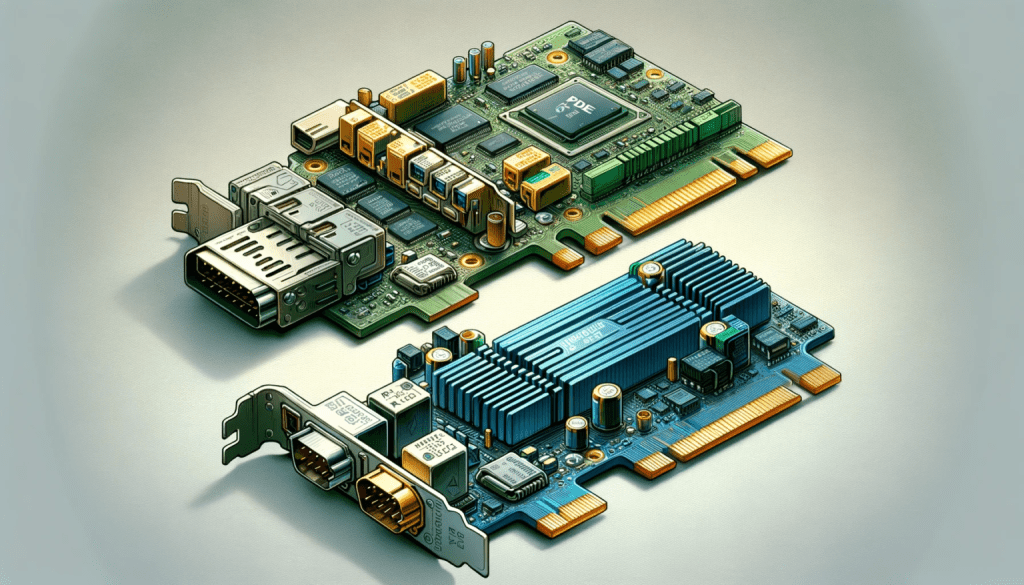
  • The Case Of High-Speed Data Transfer Between Semiconductor Components: PCIe VS CXL

    Image Generated Using DALL-E


    Introduction To PCIe:

    Peripheral Component Interconnect Express (PCIe) is a high-speed serial computer expansion bus standard designed to replace the older PCI, PCI-X, and AGP bus standards. It connects high-speed components in a computer, such as graphics cards, SSDs, and network cards. Unlike its predecessors, PCIe provides higher data transfer rates and is more flexible regarding the layout of the physical connections. It operates using a point-to-point topology, with separate serial links connecting each device to the host, which reduces latency and increases data transfer efficiency.

    Pros of PCIe:

    Higher Bandwidth: PCIe offers significantly higher bandwidth than older standards like PCI and AGP (Accelerated Graphics Port), allowing faster data transfer between components.

    Scalability: The standard supports various configurations (x1, x4, x8, x16), enabling devices to use the number of lanes that best matches their performance requirements.

    Lower Latency: The point-to-point architecture reduces latency as each device has a dedicated connection to the host.

    Backward Compatibility: PCIe is backward compatible, allowing newer devices to work with older hardware, albeit at lower performance.

    Flexibility: It supports various devices. It is also widely used in consumer and enterprise environments.

    Cons of PCIe:

    Cost: PCIe devices and motherboards are more expensive than their older PCI or AGP counterparts.

    Complexity: The increased performance and capabilities come with increased complexity in design and implementation.

    Physical Space: Higher bandwidth versions like x16 slots can take up more physical space on motherboards, limiting the number of places available.

    Power Consumption: High-performance PCIe devices, especially GPUs, can consume significant power, requiring better power supply and cooling solutions.

    Upgradability Issues: Some older motherboards might not support the latest versions of PCIe, limiting upgrade options.

    Future of PCIe:

    The future of PCIe is promising, with continuous development to increase bandwidth and efficiency. PCIe 5.0 and upcoming standards like PCIe 6.0 and 7.0 are set to offer even higher bandwidth and performance improvements, catering to the growing demands of data centers, AI, and high-performance computing. The adoption of PCIe in emerging technologies like autonomous vehicles is broadening its applications beyond traditional computing. Moreover, integrating advanced features like increased data security and power management will likely make PCIe more versatile and sustainable for future technology needs.


    Picture By Chetan Arvind Patil

    Introduction To CXL:

    Compute Express Link (CXL) is an open standard interconnect for high-performance computing components. It is built on the PCI Express (PCIe) physical and electrical interface but is distinct in its operations and objectives. CXL focuses on creating high-speed, efficient links between the CPU and workload accelerators like GPUs, DPUs, FPGAs, and memory expansion devices. CXL addresses the high-bandwidth, low-latency needs of next-generation data centers and computing applications, facilitating efficient sharing of resources and improved performance.

    Pros of CXL:

    High Bandwidth And Low Latency: CXL provides high bandwidth and low-latency communication between the CPU and connected devices, crucial for data-intensive tasks.

    Memory Coherency: One of the critical features of CXL is its support for memory coherency, allowing devices to share memory resources efficiently.

    Scalability: CXL supports various device types and sizes, making it highly scalable for different computing demands.

    Future-Proofing: As an evolving standard, CXL is future-proof, with capabilities to support upcoming computing needs in AI, machine learning, and big data analytics.

    Interoperability With PCIe: Since the PCIe infrastructure inspires CXL, it leverages the widespread adoption and existing ecosystem of PCIe, easing integration and adoption.

    Cons of CXL:

    Complexity In Implementation: Implementing CXL can require significant hardware design and architecture changes.

    Compatibility Issues: While CXL is compatible with PCIe, there may be compatibility issues with existing hardware that must adopted for CXL.

    Limited Adoption Currently: As a relatively new technology, CXL is still in the early stages of adoption, which might limit its immediate availability and support.

    Cost Implications: The Adoption of CXL could imply additional costs in terms of hardware upgrades and data center reconfigurations.

    Requirement For Newer Hardware: To leverage CXL’s benefits, newer CPUs and devices that support the standard are required, which may only be feasible for some organizations.

    Future of CXL:

    The future of CXL looks promising and is poised to play a significant role in the evolution of data center architectures and high-performance computing. As the demand for faster data processing and improved memory access grows, CXL will become more prevalent in new CPU architectures. Its ability to efficiently connect CPUs with high-speed accelerators and memory expanders aligns well with AI, machine learning, and significant data trends. Ongoing development and refinement of the CXL standard and growing industry support suggest that CXL will become a key technology in enabling more flexible, efficient, and robust computing systems.


    Comparison of PCIe and CXL:

    Below table highlights the main technical differences and similarities between PCIe and CXL. PCIe is a more general-purpose interface with a broad range of applications. At the same time, CXL is specialized for high-speed, coherent connections between CPUs and specific types of accelerators or memory expanders. The development and adoption of both technologies are continually evolving, reflecting the changing demands of computer hardware and data processing.

    Features
    Specification
    PCIe (PCI Express)CXL (Compute Express Link)
    Purpose General-purpose high-speed I/O interfaceHigh-speed interconnect for CPU-to-device communication and memory coherency
    Introduced 20032019
    Based On Original PCIe standardsBuilt on PCIe 5.0 physical and electrical interface
    Bandwidth (Per Lane) PCIe 5.0: 3.94 GB/s, PCIe 6.0: 7.56 GB/s, PCIe 7.0: 15.13. GB/sBased on underlying PCIe standard; same as PCIe
    Topology Point-to-pointPoint-to-point
    Lanes x1, x4, x8, x16, x32Based on PCIe, typically x16
    Max Throughput PCIe 5.0: 63.00 GB/s (x16), PCIe 6.0: 121 GB/s (x16), PCIe 7.0: 242 GB/s (x16)Based on PCIe lanes; subject to the PCIe version used
    Use Cases Wide range: GPUs, SSDs, Network Cards, etc.Primarily for workload accelerators (GPUs, FPGAs), memory expanders
    Key Features Scalability, backward compatibility, high bandwidthMemory coherency, low latency, high-speed CPU-device interconnect
    Power Management Advanced power management featuresInherits PCIe’s power management and adds advanced features for connected devices
    Market Adoption Widespread in consumer and enterprise hardwareEmerging, primarily in data centers and high-performance computing
    Backward Compatibility Yes, with previous PCIe versionsCompatible with PCIe, but specific features require CXL-compatible hardware
    Security Depends on implementation; no inherent security layerPotentially includes support for secure device sharing and memory protection
    Future Development Continued bandwidth improvements (PCIe 6.0 and beyond)Increasing adoption, integration with AI and ML applications, and further development of memory coherency features

    In conclusion, while sharing some foundational technologies and physical interfaces, PCIe and CXL serve distinct purposes in the computing landscape.

    The interplay between PCIe and CXL in the future of computing is significant. PCIe continues to serve as the backbone for general hardware connectivity.

    At the same time, CXL will enhance the capabilities of high-end computing systems, addressing specific challenges in memory access and device communication.

    As technology advances, the integration and co-evolution of PCIe and CXL will be crucial in shaping the next generation of computing architectures and systems.


  • The Quick Guide On Semiconductor Powered AI Accelerator

    Image Generated Using DALL-E


    An AI Accelerator is specialized hardware designed to process artificial intelligence (AI) tasks efficiently. These accelerators are specifically optimized to handle computations related to machine learning and deep learning algorithms, which are the core of most modern AI applications.

    Key features and purposes of AI Accelerators include:

    Efficiency: Designed to be more efficient than general-purpose processors like CPUs (Central Processing Units) for AI tasks. This efficiency comes from faster processing times due to higher throughput via multiple processing elements.

    Parallel Processing: AI algorithms benefit from similar processing capabilities, especially those in neural networks. AI accelerators often have architectures that support high degrees of parallelism, allowing them to process multiple operations simultaneously.

    Optimized Operations: AI accelerators get optimized for the types of mathematical operations most common in AI workloads, such as matrix multiplication and vector operations, which are crucial for neural network computations.

    Memory Bandwidth: High memory bandwidth is essential for AI workloads, and these accelerators often have specialized memory architectures to support fast data access.

    Scalability: AI accelerators can be scaled to support larger models and datasets, which is vital as the complexity of AI tasks continues to grow.

    These features make AI accelerators indispensable in various applications, ranging from natural language processing and image recognition to autonomous vehicles and advanced analytics, driving innovation and efficiency in AI development and deployment.


    Picture By Chetan Arvind Patil

    AI accelerators, despite their numerous advantages in enhancing the performance of AI and machine learning tasks, also come with certain drawbacks:

    High Cost: AI accelerators, especially the more advanced models, can be expensive. This high cost can be a barrier for smaller companies and startups needing more money for such investments.

    Specialized Hardware Requirements: Since these accelerators are specialized hardware, integrating them into existing systems can sometimes be challenging. They may require specific motherboards, power supplies, and cooling systems, which adds to the complexity and cost.

    Limited Flexibility: Some AI accelerators, particularly ASICs like TPUs, are highly optimized for specific tasks or computations. This specialization can limit their flexibility, making them less suitable for a broader range of applications or emerging AI algorithms requiring different computational capabilities.

    Software Ecosystem And Compatibility: AI accelerators rely heavily on software and frameworks compatible with their architecture. This dependency means that changes or updates in software could necessitate adjustments in the hardware or vice versa, potentially leading to compatibility issues.

    Complexity In Programming And Maintenance: Programming AI accelerators requires specialized knowledge and skills, particularly for optimizing the performance of AI models. Additionally, maintaining these systems, both in terms of software and hardware, can be complex and resource-intensive.

    Power Consumption And Heat Generation: High-performance AI accelerators can consume significant power and generate considerable heat, especially in large data centers. It necessitates sophisticated cooling solutions and can lead to higher operational costs.

    Scalability Challenges: While AI accelerators are scalable, scaling them to extensive systems can be challenging and expensive, especially in data center environments where thousands of accelerators might be required, leading to increased complexity in infrastructure, power, and cooling requirements.

    Rapid Obsolescence: AI and machine learning are advancing rapidly, and hardware can quickly become obsolete as more new models emerge. This fast pace of development can make it challenging for organizations to keep up with the latest technology without significant ongoing investment.

    In conclusion, AI accelerators significantly advance artificial intelligence and machine learning, offering unparalleled efficiency and performance for complex computational tasks. These specialized hardware components have become crucial in powering a wide range of AI applications, from deep learning models in data centers to real-time processing in edge devices.

    While they offer substantial benefits regarding processing speed and energy efficiency, challenges, such as high cost, specialized hardware requirements, limited flexibility, and rapid obsolescence, must be carefully considered. As the AI landscape continues to evolve rapidly, AI accelerators stand as a testament to the ongoing synergy between hardware innovation and software development, driving forward the capabilities and applications of AI technology in an increasingly digital world.


  • The Skills Needed To Improve The Yield And Test Time Of A Semiconductor Product

    Image Generated Using DALL-E


    In the fast-paced world of semiconductor product development, two metrics stand out as pivotal to the success and efficiency of manufacturing: yield and test time.

    Yield, the percentage of functional chips in a production batch, directly influences the cost-effectiveness and viability of semiconductor products. Simultaneously, test time, the duration spent verifying the functionality and reliability of these chips, plays a crucial role in determining the throughput and overall efficiency of the production process.

    Thus, it is essential to understand the intricacies of yield and test time in semiconductor manufacturing, exploring their significance, challenges, and the vital skills required to optimize these critical factors.

    Yield In Semiconductor Product Development:

    Yield refers to the proportion of functional chips produced from a batch in semiconductor manufacturing. It’s a critical factor in determining the cost-effectiveness of the manufacturing process because higher yields mean more functional chips per batch, reducing the cost per chip.

    The complex semiconductor manufacturing process, involving steps like oxidation, coating, lithography, and etching, poses significant yield challenges. Each wafer undergoes hundreds of high-precision processes over three to six months and must pass stringent quality tests.

    Yield analysis has evolved from a simple comparison of good and bad units to a more sophisticated approach involving data science. This deeper analysis helps in understanding and mitigating a range of factors that contribute to yield issues.

    Test Time In Semiconductor Product Development:

    Test time in semiconductor manufacturing refers to the duration spent testing the chips for functionality and reliability. Reducing test time is essential for decreasing running costs and improving manufacturing throughput.

    Key strategies to reduce test time include eliminating redundant tests, reordering tests to screen out significant failures early, and sample testing or removing “always passing” tests. This approach requires a deep understanding of device behavior.

    Virtual testing methodologies can significantly reduce the overall product development time for semiconductors. It allows for earlier detection of potential issues and streamlines the development process.​


    Picture By Chetan Arvind Patil

    Skills Needed To Improve Yield And Test Time:

    Deep Technical Knowledge: Understanding the intricate details of semiconductor manufacturing processes and the behavior of devices is essential. This knowledge enables engineers to identify and address yield issues effectively and to streamline testing processes.

    Data Analysis And Yield Modeling: Data science and analytics skills are crucial for yield analysis. Engineers must use yield modeling tools to identify design and process-related issues.

    Design For Testability (DFT) Expertise: Engineers should have expertise in designing chips with testability in mind. It involves creating more straightforward test and diagnose designs, thus improving yield and reducing test time.

    Process Optimization: Skills in process optimization, removing redundant steps in manufacturing and testing, are vital. It includes reengineering test flows and optimizing test programs.

    Familiarity With Virtual Testing Tools: Knowledge of virtual testing methodologies and tools can help reduce product development time and early issue detection.

    Adaptability To Technological Advances: As semiconductor technology evolves, staying updated with the latest methodologies and tools is crucial for continuous yield and test time improvement.

    Collaborative Skills: Working effectively with cross-functional teams, including design, manufacturing, and quality assurance, is essential for holistic improvements in yield and test time.

    In conclusion, mastering the aspects of yield and test time is indispensable in the realm of semiconductor manufacturing. The journey from understanding the complexities of these factors to effectively implementing strategies for improvement requires a blend of technical acumen, analytical prowess, and innovative thinking.

    Professionals in the field must continually evolve, embracing new methodologies and technologies to stay ahead in this dynamic industry. The enhancement of yield and test time bolsters production efficiency and serves as a cornerstone for the business success and technological advancement of semiconductor products.


  • The Challenges And Roadblocks For Indian Semiconductor Manufacturing Industry

    Image Generated Using DALL-E


    The semiconductor industry, often termed the backbone of modern technology, is crucial for advancing and sustaining almost all major sectors, from telecommunications to automotive. As the world rapidly transitions towards a more digitized future, the significance of semiconductors has escalated, leading to a global race in semiconductor manufacturing.

    With its ambitious plans and vast potential, India has entered this race. However, the journey to becoming a semiconductor powerhouse has numerous challenges. Below is a comprehensive overview of the multifaceted hurdles that the Indian semiconductor industry currently faces, from infrastructure and skilled workforce shortages to global competition and policy constraints.

    Skilled Workforce Shortage: India has a large pool of design engineers. However, semiconductor engineers are scarce with expertise in device physics and process technology, which are essential for chip fabrication and manufacturing​​.

    High Capital Investment: Setting up a semiconductor manufacturing unit involves enormous investment, with the cost of building a new fab estimated to be over one billion U.S. dollars. Additionally, these facilities require well-trained teams and the capacity to support large production volumes from the outset​​. Currently, India is behind in both.

    Global Competition: India faces stiff competition from established semiconductor manufacturing hubs like China, Taiwan, and South Korea. Building a complete domestic value chain for semiconductors is challenging, mainly when a significant portion of this value chain is outside of India.

    Government Incentives And Policy Response: The Indian government’s incentives under schemes like the “Modified Scheme for Semiconductors and Display Fab Ecosystem” have received a lukewarm response, suggesting that the incentives might not be sufficiently attractive compared to other geographies. There is skepticism among global chip giants regarding setting up manufacturing in India​​.


    Picture By Chetan Arvind Patil

    Late Entry: India missed early opportunities to establish itself in the semiconductor industry. This delay has made it challenging to catch up with countries that started developing their semiconductor industries decades ago, such as Taiwan​​.

    Comparison: Taiwan, a global leader in semiconductor manufacturing, offers a stark contrast to India. It has a complete semiconductor manufacturing, packaging, and design ecosystem supported by skilled labor, investment in infrastructure, technological expertise, and strong government backing. In contrast, India struggles with infrastructure limitations and needs an established ecosystem.

    Cost Competitiveness: Global chip manufacturers are hesitant to operate in India due to cost competitiveness and infrastructure challenges. India’s ability to compete with established semiconductor manufacturing hubs regarding cost-effectiveness and access to advanced technology is a significant hurdle​​.

    Logistical Challenges: Semiconductor manufacturing facilities, or ‘fabs,’ require significant space, uninterrupted power, and a substantial water supply. India’s infrastructure, regarding reliable power supply and water resources, is still developing. Additionally, the proximity of airports and customs facilities is crucial for importing and exporting key components. In India, customs clearance can be time-consuming, and the lack of developed infrastructure around potential fab sites poses a challenge​​.

    As India strives to carve out its niche in the semiconductor industry, it becomes clear that overcoming these challenges requires a multifaceted approach. It involves significant government support in terms of policy-making and financial incentives and a focus on building a skilled workforce and robust infrastructure. Collaborations with global leaders in the field, fostering a conducive environment for R&D and ensuring a steady supply chain are equally critical.

    In conclusion, the journey of the Indian semiconductor industry is symbolic of the broader challenges emerging economies face in high-tech sectors. The lessons learned, and the successes achieved in this endeavor will shape India’s technological capabilities and serve as a blueprint for other nations aspiring to enter such complex and competitive fields.


  • The Ways In Which OpenAI Can Reinvent Semiconductor Chip Development

    Image Generated Using DALL-E


    OpenAI’s involvement in semiconductor chip development could mark a significant shift in the industry, bringing about advancements in silicon design, silicon software stack development, R&D investment, and the application of GenAI in chip design.

    However, the complexity and cost of chip development have escalated, posing significant challenges. It is where OpenAI, with its cutting-edge AI technologies, can play a transformative role.

    Let’s explore how OpenAI can revolutionize the various aspects of semiconductor chip development.

    Empowering Chip Development Teams With AI:

    The first area where OpenAI can make a substantial impact is in augmenting the capabilities of chip development teams. AI models, especially those developed by OpenAI, can analyze vast amounts of data from previous chip designs, manufacturing processes, and performance metrics.

    This analysis can lead to insights that would only be possible for human teams to discern due to the sheer volume and complexity of the data.

    For instance, AI can predict how minor changes in the design might affect the chip’s overall performance and energy efficiency. This predictive capability can significantly reduce the time and cost of trial-and-error methods traditionally used in chip design.

    Revolutionizing The Software Stack For Chip Design:

    The software stack used in chip design, from schematic capture to physical layout, is ripe for innovation. OpenAI’s models can be integrated into these software tools to enhance functionality.

    For example, AI can automate parts of the layout process, optimizing the placement of components to minimize signal delays and power consumption while maximizing performance.

    Moreover, AI can assist in the verification process, quickly identifying potential errors or inefficiencies in the design. This integration can drastically reduce the time to market for new chips and improve their overall quality and performance.


    Picture By Chetan Arvind Patil

    Investing In R&D And Knowledge Building:

    OpenAI’s involvement in semiconductor chip development is not just about directly applying AI technologies by building AI silicon chips but also about fostering a deeper understanding of the field.

    By investing in research and development, OpenAI can help uncover new design methodologies and manufacturing techniques that could revolutionize the industry.

    Furthermore, OpenAI can contribute to knowledge building around silicon chip design and manufacturing. It could involve developing AI models that simulate different manufacturing processes or predict the performance of new materials, thereby providing valuable insights to researchers and engineers.

    GenAI For Silicon Chip Design:

    The most futuristic application of OpenAI in chip development is the concept of Generative AI (GenAI) for silicon chip design. GenAI can go beyond optimization and generate novel chip designs based on specified parameters and performance goals.

    This approach could lead to breakthroughs in chip design, uncovering configurations and architectures that humans might not conceive.

    For instance, GenAI could design chips optimized explicitly for AI workloads or ultra-efficient chips for use in smart devices. The potential here is vast, and as AI technology continues to evolve, so will its chip design capabilities.

    Integrating OpenAI’s technologies into semiconductor chip development heralds a new era of innovation and efficiency.

    By empowering development teams, revolutionizing the silicon software stack, investing in R&D, and leveraging GenAI, OpenAI can help overcome current limitations and open up new possibilities in chip design and manufacturing.

    As these technologies mature, we can expect faster, more efficient, and more powerful semiconductor chips, driving the next wave of technological advancement.


  • The Semiconductor Mobile SoC Leaders

    Image Generated Using Adobe Firefly


    Several companies have established themselves as prominent mobile System-On-A-Chip (SoC) technology players. The landscape is characterized by intense competition and rapid innovation, leading to the continuous evolution of SoC capabilities.

    Some of the leading SoC vendors that are competing to capture a share of the mobile market are:

    Qualcomm: Known for its Snapdragon series, Qualcomm is a significant player in the mobile SoC market. Its SoCs are renowned for their performance, energy efficiency, and integration of advanced features like 5G connectivity and AI capabilities.

    Apple: Apple’s custom SoCs, such as the A-series used in iPhones and iPads, are highly regarded for their performance and efficiency. Apple’s control over hardware and software allows for optimized integration, resulting in impressive computational capabilities.

    Samsung: Samsung Electronics, with its Exynos line of SoCs, is a key competitor in the market. These SoCs are used in various Samsung mobile devices and are known for integrating custom CPU and GPU cores.

    MediaTek: MediaTek has gained significant market share, especially in the mid-range and budget segments. Its Helio and Dimensity series of SoCs balance performance and cost-effectiveness, making them popular among various smartphone manufacturers.

    Huawei: Through its HiSilicon division, Huawei produces the Kirin series of SoCs. These chips are primarily used in Huawei’s range of smartphones and are known for their AI processing capabilities and 5G technology.

    Google: Google has entered the SoC market with its custom Tensor chip, which powers its Pixel phones. The Tensor chip focuses on machine learning and AI tasks, leveraging Google’s expertise.

    These companies have contributed to advancing mobile SoC technology through unique strengths and innovations. The choice of SoC often depends on the specific requirements of the device, including performance needs, power efficiency, connectivity options, and cost constraints.


    Picture By Chetan Arvind Patil

    The future of mobile SoC technology is poised for significant advancements, driven by evolving consumer demands and technological innovations. As we look toward the end, several key trends and developments are likely to shape the trajectory of mobile SoC design and capabilities:

    Advanced Process Technologies: The progression towards smaller nanometer (nm) fabrication processes will continue. This evolution enables more transistors to be packed into the same space, enhancing performance and energy efficiency. Leading-edge process technologies like 3nm and beyond are to be adopted.

    AI And Machine Learning: Mobile SoCs will likely see increased integration of dedicated AI and machine learning hardware. It will enhance on-device processing for image and voice recognition, augmented reality (AR) experiences, and personalized user experiences.

    Next-Gen Graphic Processing: As mobile gaming and multimedia consumption grow, SoCs will integrate more powerful GPUs capable of supporting advanced graphics, high refresh rate displays, and improved AR/VR experiences.

    5G And Beyond: The integration of 5G connectivity will become standard in mobile SoCs, offering faster data speeds and lower latency. Future developments may focus on optimizing 5G performance and beginning the groundwork for 6G technology.

    Energy Efficiency And Battery Life: With the increasing demand for power from high-performance applications, energy efficiency remains a critical focus. Future SoCs must balance performance with power consumption to extend battery life.

    Custom And Specialized SoCs: Companies may increasingly develop custom SoCs tailored to specific device needs or market segments. This trend is already visible with companies like Apple and Google developing their chips.

    The future of mobile SoCs will be a blend of technological advancements and adaptations to changing user needs and global trends.

    The continual push for innovation in this space suggests an exciting and dynamic future for mobile computing technology.


  • The Semiconductor Lithography Race: NIL VS EUV

    Image Generated Using Adobe Firefly


    In semiconductor manufacturing, lithography is a pivotal process. It involves transferring circuit patterns onto a silicon wafer, a foundational step in creating integrated circuits (ICs).

    Two of the most advanced lithography techniques currently at the forefront of this industry are Extreme Ultraviolet (EUV) and Nanoimprint Lithography (NIL).

    Nanoimprint Lithography (NIL) and Extreme Ultraviolet Lithography (EUV) are two technologies used in semiconductor fabrication, each with advantages and challenges. Below is a comparative analysis.

    Extreme Ultraviolet Lithography (EUV):

    Technical Overview: EUV lithography employs a highly sophisticated process that uses extreme ultraviolet light (with a wavelength of approximately 13.5 nm) to etch wonderful patterns onto silicon wafers. This technology is a leap from traditional lithography, which uses deep ultraviolet light.

    Advantages: The primary benefit of EUV is its unparalleled resolution, allowing for the production of smaller, more complex ICs. It is crucial as the industry moves towards ever-smaller node sizes, particularly 5nm and below. EUV enables higher circuit density, contributing to the chips’ enhanced performance and energy efficiency.

    Challenges And Limitations: The transition to EUV has faced significant technical and financial difficulties. The development of EUV machines, such as those produced by ASML, is incredibly costly and complex. Furthermore, EUV requires highly purified materials and controlled environments to minimize photon absorption by air or contaminants. The technology also faces throughput limitations, as EUV processes are generally slower than their deep UV counterparts.

    Nanoimprint Lithography (NIL):

    Technical Overview: NIL is a form of lithography that physically imprints a pattern onto a substrate using a mold or stamp. This method is similar to traditional printing techniques but at a nanometer scale.

    Advantages: NIL’s main advantage lies in its simplicity and cost-effectiveness compared to EUV. It can achieve high-resolution patterns without complex light sources or optics. NIL is particularly promising for applications that require large-area patterning, such as advanced sensors and display technologies.

    Challenges And Limitations: NIL’s primary challenge is defectivity and uniformity over large areas. The physical nature of the imprinting process makes it susceptible to defects caused by particle contamination or imperfections in the mold. Maintaining uniform pressure and temperature across the entire wafer during imprinting is a significant challenge.


    Picture By Chetan Arvind Patil

    Comparative Analysis:

    Resolution And Precision: While both techniques aim to push the boundaries of miniaturization, EUV currently leads in terms of resolution and is more suited for the most advanced logic and memory devices.

    Throughput And Cost: NIL offers potentially higher throughput at a lower cost, making it an attractive option for specific semiconductor applications, particularly those not requiring the extreme miniaturization capabilities of EUV.

    Application Suitability: EUV is helpful for high-end, cutting-edge semiconductor fabrication, especially for CPUs and GPUs. On the other hand, NIL finds its niche in less critical layers of ICs and in specialized applications like photonics and biochips.

    The race between EUV and NIL is not a straightforward competition but rather a complementarity of technologies, each serving unique semiconductor market segments. As the industry progresses, we may see advancements in both technologies, potentially leading to hybrid approaches or innovations entirely. The choice between EUV and NIL will depend on specific application requirements, cost constraints, and technological advancements.

    As the semiconductor industry continues to evolve, staying abreast of these developments is crucial for manufacturers, technologists, and stakeholders in this dynamic field.