Photo by Patrick Perkins on Unsplash
The semiconductor market has always followed the seesaw mode. With a seesaw, there are time intervals when the market has high demand followed by low demand. This trend impacts the semiconductor in different possible ways, and one of them is the long-term product development strategy.
There is no easy way to control such a trend. The semiconductor industry should be pre-prepared and adapt based on the market feedback. It requires a mitigation plan, which should not impact product development and manufacturing.
Market: Semiconductor Market Is Always In Seesaw Mode.
Impact: Market Seesaw Impacts Long-Term Projections.
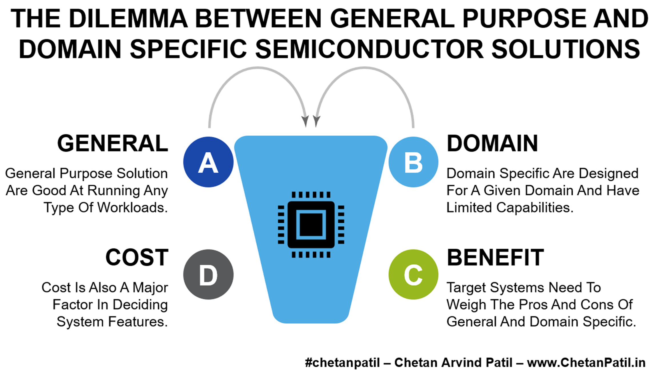
The semiconductor market seesaw raises questions about whether a focused market approach is good or bad. Mainly for those semiconductor companies that are only catering to a specific market.
One better way to manage the impact of the market is to diversify the products. Such a strategy enables companies to be more resilient, which benefits the industry during the phases when the market demand is not as expected.

In the coming years, the semiconductor industry will need to develop trillion more silicon devices. It requires robust planning that balances the design and manufacturing capacity.
For such targets, the market seesaw movement also plays a crucial role. Thus, raising the need to capture the upward/downward trend before it occurs, as it can allow more proactive planning than reactive.
Future: More Robust Future Planning Is Required.
Trend: Seesaw Trend Is Expected To Continue Forever.
The trend and the future of the semiconductor market will always keep changing. Thus, making it difficult to capture the ripple effect. It presents a unique challenge and opportunity for companies to develop predictive tools that can capture the future trend and then alert in advance on how to manage operational activities.
Market impact on the semiconductor or any other industry will be a deciding factor in driving the future course of action. What is crucial is to capture the such trend and then divert resources to mitigate any ripple effect. More so when the impact is on a high-tech industry like a semiconductor.