Photo by Louis Reed on Unsplash
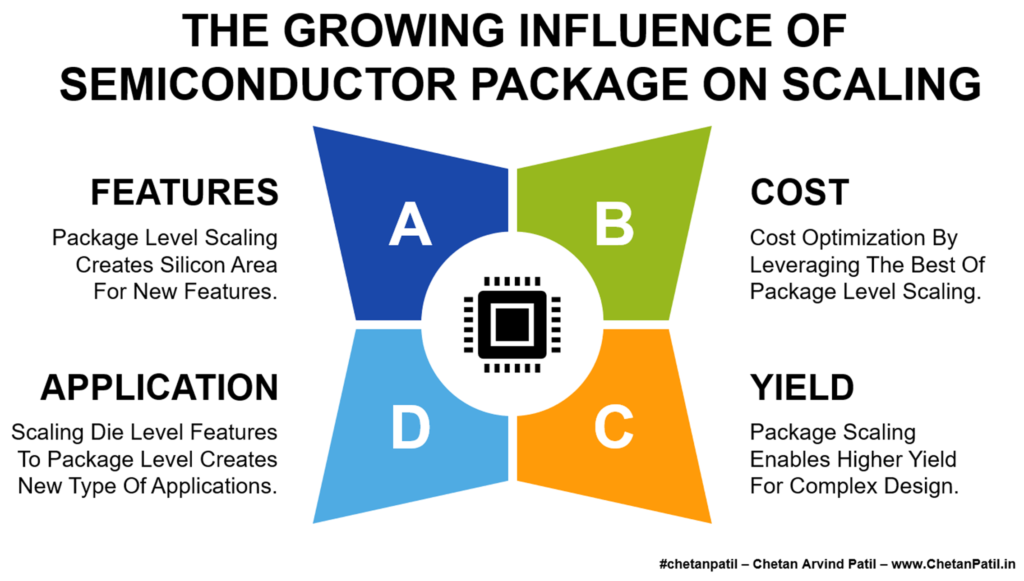
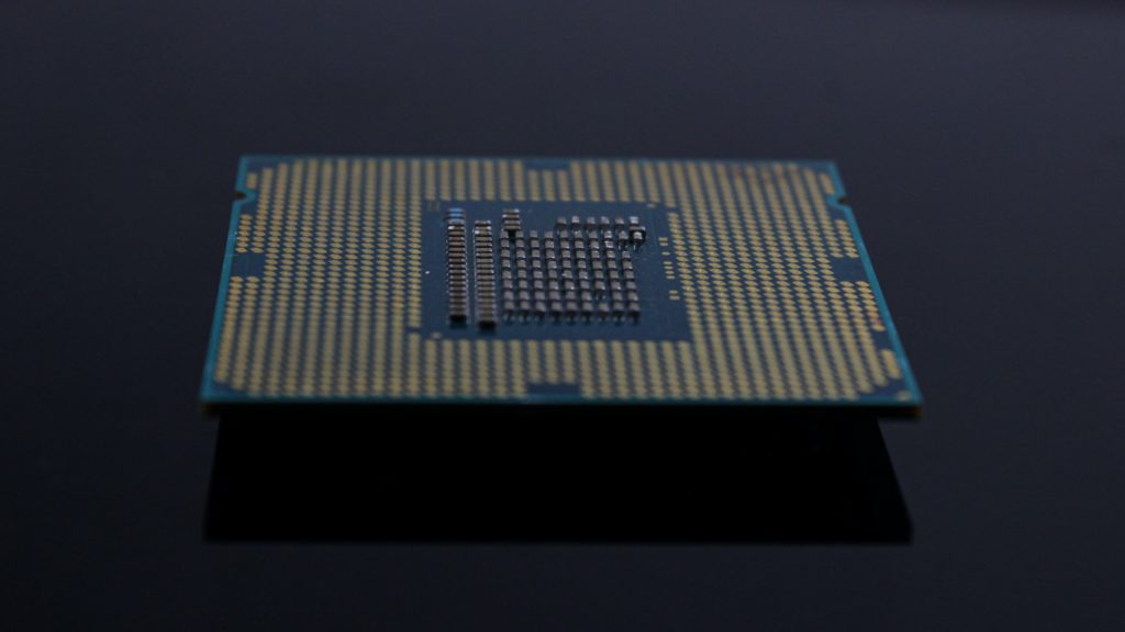
Chiplets are changing the way complex products like XPUs getting designed and manufactured. Its impact is how modular the new XPU solutions are becoming. This modularity is paving the way for new-age IP-driven XPU design and manufacturing and opening up features that were not easy to deploy due to the need for the aggregated approach.
As with any new semiconductor process and technology, the vital factor is the long-term impact of such new solutions. In the case of chiplets, it has already started to impact design and manufacturing methods.
The positive long-term impact of chiplets is providing the ability for XPU developers to enable solutions in the angstrom era by leveraging the disaggregated approach. It is also opening up a new design approach that allows chip architects to leverage different types of IP blocks and also provides the ability to enhance block-level processing capability due to the disaggregated manufacturing.
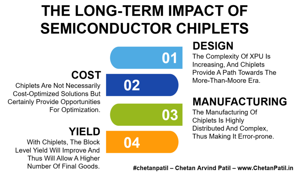
Design: The complexity of XPU is increasing, and chiplets provide a path towards the More-Than-Moore era.
Cost: Chiplets are not necessarily cost-optimized solutions but certainly provide opportunities for optimization.
From the cost point of view, chiplets may be costly to manufacture due to the die level disaggregation that will require multiple silicon wafers and capacity. The manufacturing flow will also become more complex. Until the chiplet adoption speeds up, the early adopters will have to spend more capital.
However, as the adoption increases, the manufacturing processes are bound to become optimized. It will then drive better cost-optimized manufacturing of chiplets-driven XPUs.
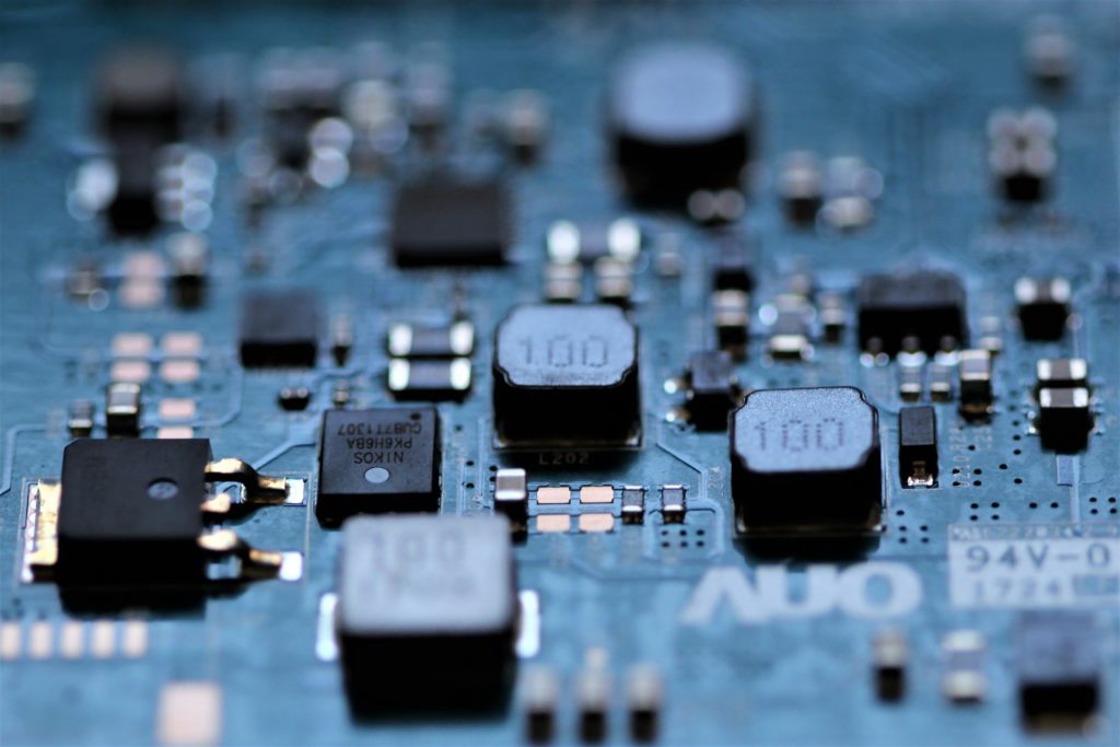
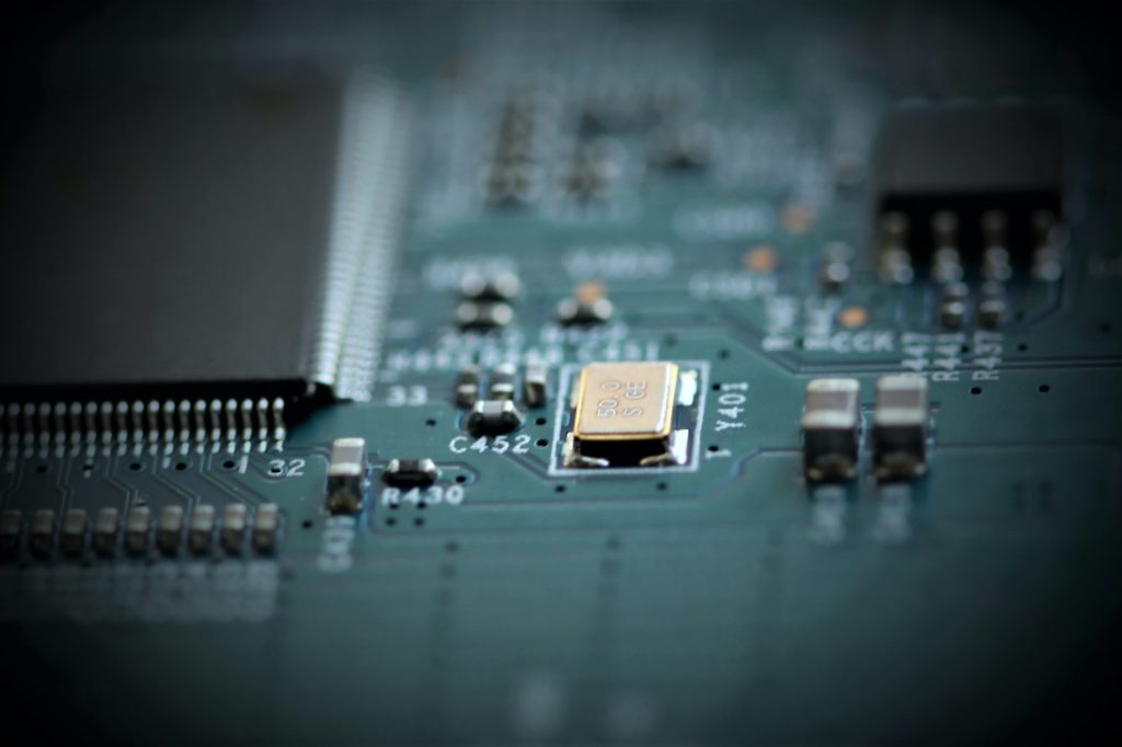
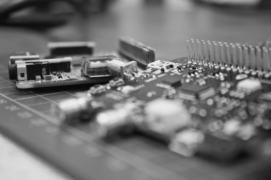
Distributed processing of chiplets at the manufacturing side brings new challenges. More so when the packaging of chiplets becomes a critical process. The complex manufacturing flow on the packaging side can drive a higher error rate if the process is not validated correctly before mass production.
There are processes available to ensure the new manufacturing process (chiplets) leads to positive results. However, until the chiplets-inspired chips are mass-produced, there will always be a possibility of errors and such errors will impact yield and cost.
Manufacturing: The manufacturing of chiplets is highly distributed and complex, thus making it error-prone.
Yield: With chiplets, the block level yield will improve and thus will allow a higher number of final goods.
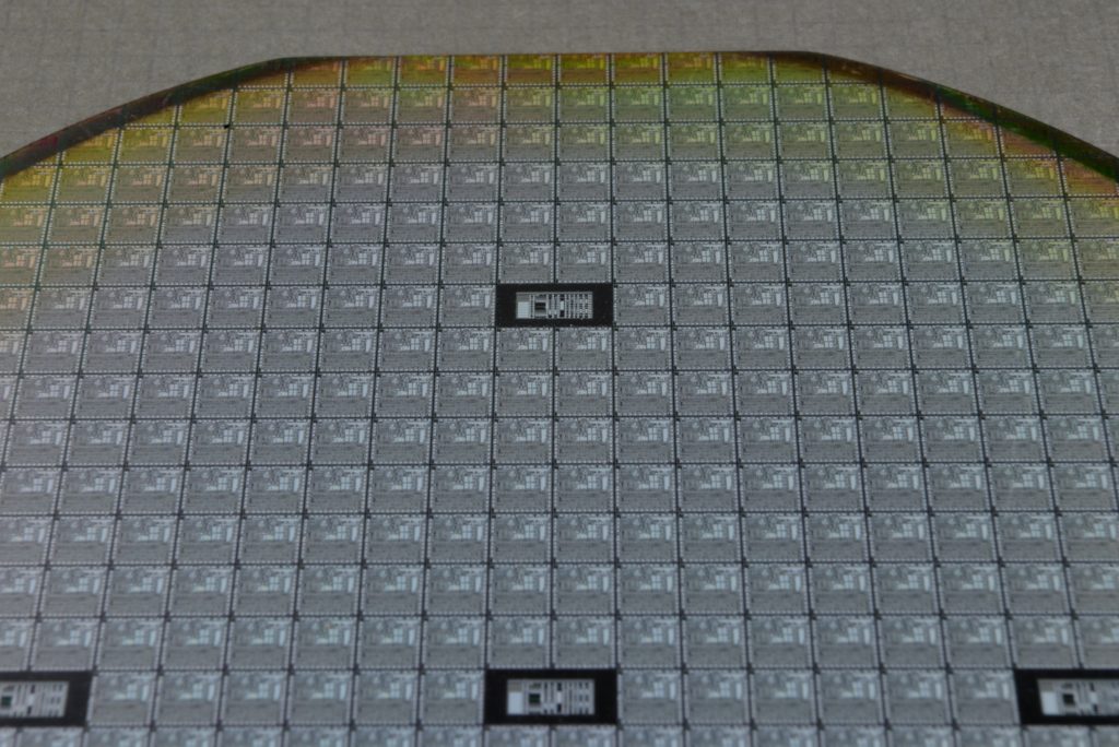
The aggregated approach of XPU design and manufacturing does not often lead to higher yields. Disaggregated manufacturing of chiplets enables higher yield. Mainly due to the ability to take the complex critical blocks as separated die.
Chiplets design and manufacturing methods are still in the early days. As adoption and usage grow, the positive and negative long-term impacts will be more visible. Meanwhile, today, chiplets are indeed the most promising More-Than-Moore era solutions.