Image Generated Using Nano Banana
The Shifting Foundations Of Semiconductor Productivity
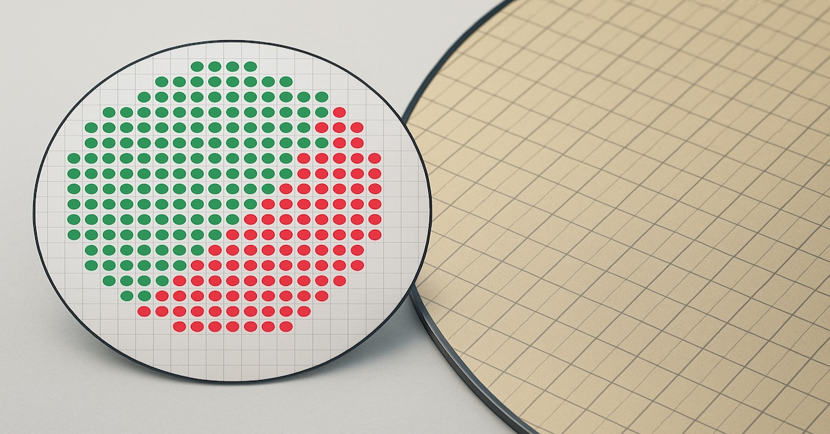
Productivity in semiconductors was once anchored in a predictable formula in which each new node delivered higher transistor density, better performance per watt, and stable cost per transistor. That engine is weakening.
Design complexity has surged, stretching development cycles from roughly 6-12 months to 12-24 months or more for leading-edge SoCs, driven by more than 1.5 billion verification cycles and verification workloads that account for 55 percent of total effort.
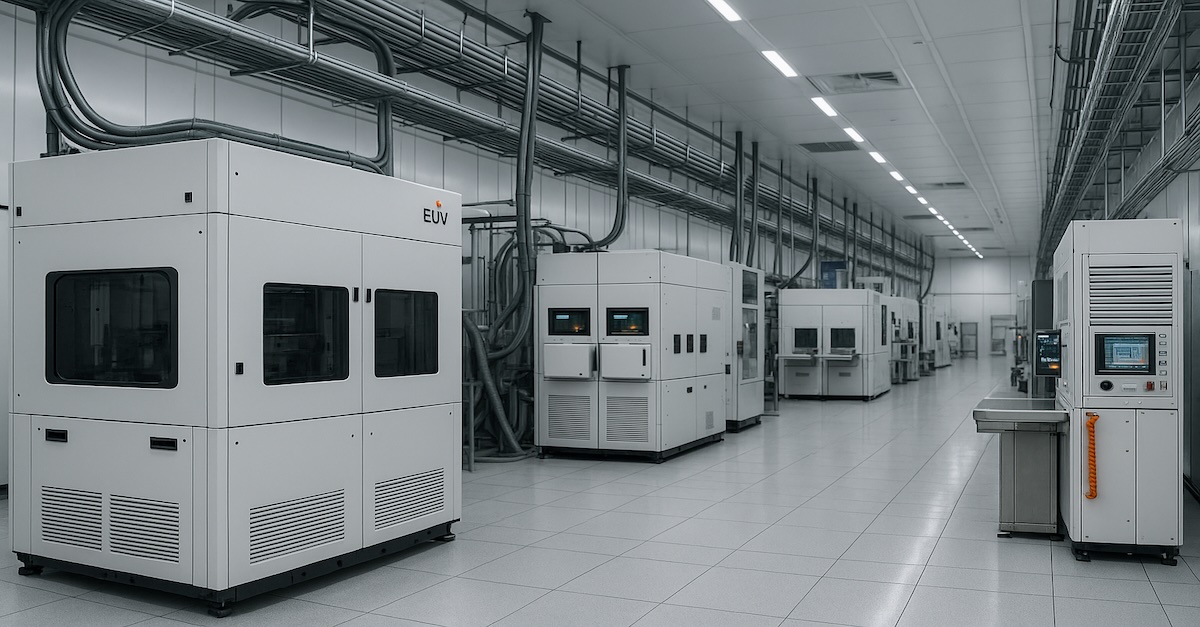
Manufacturing is under similar strain, as EUV tools consume nearly 1 megawatt per scanner, require over 50% uptime for economic breakeven, and demand more than planned service interventions per year. Costs per reticle, mask, and process layer continue to rise, breaking the traditional assumption that fabs scale efficiently through capital expansion.
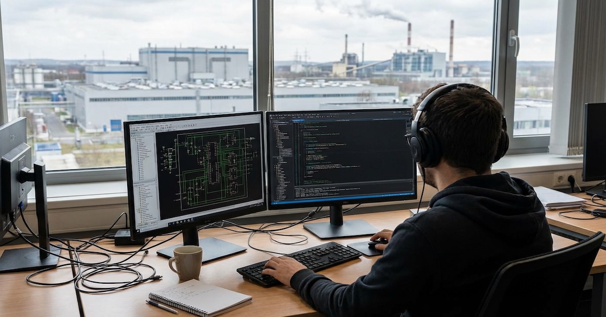
Talent constraints further intensify the challenge. Deloitte’s Semiconductor Workforce Study forecasts a shortage of more than 1 million skilled workers by 2030, with acute gaps in RF, physical, lithography, and packaging. Many of these jobs require 3 to 5 years of training before reaching full productivity, meaning that new fabs deliver immediate capital capacity but delayed human-capacity scaling.
As complexity, cost, and workforce requirements outpace traditional efficiency levers, the industry faces a widening productivity gap reflected in slower node adoption, rising unit costs, and delayed revenue realization. Closing this gap requires a fundamental rethinking of design automation, manufacturing operations, and the leverage of engineering.
Why The Productivity Gap Matters For The Global Semiconductor Business
The productivity gap has significant economic consequences across the semiconductor value chain. Time-to-market pressure is among the most critical. As semiconductor delivery timelines stretch, downstream industries slow correspondingly, creating friction across entire product ecosystems.
Capital efficiency is also under strain. A modern 5 nm fab requires more than $ 20 billion in investment, yet wafer starts per tool are growing more slowly than capital intensity. SEMI’s 2024 World Fab Forecast reports that leading-edge capacity grew only 6 percent in 2023 while capital intensity rose nearly 12 percent, meaning each incremental wafer requires disproportionately higher investment.
Combined with slowing node transitions and reduced cost-per-transistor improvements, the traditional economic benefits of scaling are diminishing. This puts pressure on business models that depend on rapid node migration, especially in high-volume mobile and compute markets.
These effects cascade across supply chains: delayed design inputs slow fab loading, manufacturing bottlenecks delay customer shipments, and product cycles across electronics, automotive, cloud, and AI sectors lose momentum.
The semiconductor productivity gap, therefore, acts as a drag on global innovation, competitiveness, and economic growth.
How AI And Automation Can Close The Semiconductor Productivity Gap
Artificial intelligence and automation are emerging as the most powerful tools to bridge the productivity divide. The goal is not only faster execution but also more thoughtful execution. AI has the potential to collapse design loops, optimize fab operations, and augment the limited engineering workforce.
In design, AI-driven EDA tools can accelerate RTL generation, automate physical design exploration, and reduce verification workloads. Google’s reinforcement learning floorplanner demonstrated a 10x reduction in layout search time in published results from Nature. AI-based verification triage systems can analyze failing regressions and automatically cluster root causes, reducing engineering debug by hours.
In manufacturing, AI-enabled process control can stabilize fabs with fewer interventions. Predictive maintenance models for etch and deposition tools can extend mean time between failures, and when fab equipment availability increases, overall fab productivity rises without proportional increases in labor or capital.
| Area | Possible AI Technique | Impact |
|---|---|---|
| RTL to GDS design | Generative RTL and automated floorplanning | Faster architecture exploration and reduced layout search time |
| Verification | Regression clustering and failure triage | Significant reduction in debug workload |
| Lithography | Dose and focus machine learning correction | Lower variation and fewer rework cycles |
| Fab equipment | Predictive maintenance using ML | Extended mean time between failures and higher uptime |
| Supply chain | AI-based demand and risk forecasting | Improved continuity and reduced inventory exposure |
The combined effect of these improvements is significant. Even moderate efficiency gains across thousands of design engineers or hundreds of fab tools produce measurable bottom-line impact. AI gives the industry new scaling levers at a time when traditional scaling is slowing.
Strategic Imperatives For A More Productive Semiconductor Future
The semiconductor productivity gap is real, expanding, and rooted in structural forces that will not correct on their own. Rapid growth in design complexity, mounting manufacturing challenges, and a global shortage of skilled engineers are stretching development cycles and reducing the economic leverage the industry once relied on.
These pressures slow innovation, raise costs, and weaken the longstanding assumption that each new node or product generation will automatically deliver meaningful productivity gains.
Addressing this gap requires coordinated action across technology, workforce, and capital strategy. AI and automation provide the most powerful levers, with the potential to create new productivity curves similar to the early years of EDA and factory automation.
Companies that embed AI-driven workflows throughout design and manufacturing will move faster, utilize capital more efficiently, and operate more resilient supply chains. By modernizing workflows and strengthening engineering leverage, the industry can rebuild the compounding productivity that once defined semiconductor progress and support the next decade of global technological growth.