Logic devices (FETs) are the building blocks of semiconductor products. Today’s silicon chip can easily have billions of these logic devices. It is also in line with Moore’s law, and today’s semiconductor technology allows the possibility of packing more logic devices without impacting the total silicon area.
Semiconductor equipment and other semiconductor technologies have also played a key role in achieving the goal of fabricating innovative logic devices. Apart from this, both academia and industry have consistently provided novel ways to design logic devices for the future requirements of semiconductor products.
The impact of these logic devices on the overall semiconductor product-driven system is high and ranges from the technical to the business aspect. It is the primary reason the semiconductor design and manufacturing houses are always coming up with techniques to improve the efficiency of logic devices.
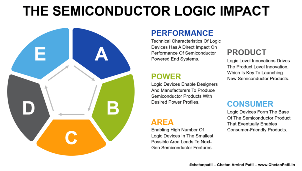
Performance: Logic devices directly impact the performance of the overall semiconductor products. The reason is the faster turn on/off time. To power performance-oriented silicon chips, underlying logic devices need to have the required characteristics that enable high performance. It is also the primary reason the industry is adopting next-gen FET devices.
Power:Several systems that do not require high-performing logic devices. Instead, they need a device that can work over different power profiles. It is usually the requirement of low-power semiconductor products. It is also where logic devices need to have smaller power footprints come into the picture and have been around for decades.
Area: The need to pack more logic devices will keep increasing due to the demand for faster processing. It is where logic devices play a crucial part and often have to evolve (technical features at the gate level) to cater to the next-gen processing demand while having minimal impact on the silicon area.
As the semiconductor industry moves towards the era where silicon chips might easily have trillions of logic devices, the need for next-gen logic devices that have minimal impact on the cost and time will grow too.
Logic devices also drive the business aspect of semiconductor products. It is in the form of products that get launched and what type of new features these products will have.
Product: New semiconductor products need to be at par with the predecessor products. It is only possible if the underlying semiconductor technology evolves as per the changing requirements. It requires advanced logic devices.
Customer:Consumer-friendly products require a good balance of internal architecture capabilities. It often ranges from response time to battery life. These two features are driven by the building blocks of the semiconductor products i.e. logic devices.
More than the semiconductor design, semiconductor manufacturing needs to invest more time and money to enable new logic devices. The majority of the investment eventually provides the next-gen solutions to the semiconductor industry at large. FinFET is one such example, which originated due to the cross-industry and academia efforts.
As the need to pack more transistors without affecting the time, area, and cost increases, the investment towards the research and development activities of the logic devices will have to increase too.
In the end, the semiconductor design and manufacturing companies will keep innovating to prepare themselves for the decades to come, and academia will also play a crucial role in promoting next-gen logic devices.
The computing industry relies on semiconductor products to enable faster processing. And, to drive real-time processing semiconductor industry has to keep innovating. This two-way hand-shake reliance has grown over the last decade (due to new software demand) and will only grow more in the decades to come.
For decades, the use case of computers (and the silicon chip inside it) has been to perform tasks that humans will take years to perform manually. However, year on year, this processing by generic systems (or XPU) has become repetitive and slow. Today, industries that rely on computational resources are looking for solutions that are adaptive, smarter, and efficient all at the same time.
Neuromorphic Computing Utilizes Semiconductors To Mimic Neuro-Biological Architectures To Drive Adaptive Computing.
Several adaptive solutions are already around. All of these rely on model-driven neural networks. However, the time and cost involved in developing such solutions are very high. To overcome these two drawbacks, both the software and the hardware industry have already embarked on the interdisciplinary process of bringing together the basic and applied science to empower the neuromorphic computing ecosystem.
Industry and academia have heavily focused on neuromorphic computing and have come up with brain-inspired silicon biological nervous systems that today can allow more accurate and real-time computation. Robotics already uses such and some other vision systems that demand a human way of processing data.
This rise of semiconductor-powered neuromorphic computing is eventually a sum of several benefits that it provides. These benefits are in line with the future requirements as required by several silicon-dependent industries.
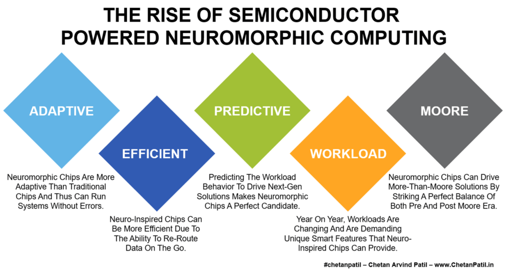
Adaptive: Real-time computation is heavily dependent on silicon chips, and over the last few decades, the silicon processing units have been rigid. Neuromorphic computing enables the development of neuro-inspired chips that can be more adaptive (and may drive error correction) and efficient than any other XPUs.
Efficient: High-performance silicon chips have to work non-stop, and that too without adding any bottlenecks. Neuro-inspired chips can provide a way to re-architect the routing protocols to make the system more efficient and bottleneck-free.
Predictive: Smart technologies are on the rise, and silicon chips need to do more than process the data as it is. On another side, traditional chips do not change after production. However, neuro-driven silicon chips provide a way to predict future workload requirements and then enable internal circuits accordingly.
There is always a question about how adaptive and predictive neuromorphic computing can be. And whether it is suited for a specific purpose only. An enterprise-grade data center with power-hungry servers might find a good fit for neuromorphic computing solutions rather than a laptop where the applications are still performing the basic operations.
Neuromorphic computing is a domain-specific solution today. As more innovative approaches come out, part of the silicon solution might get incorporated into the more generic semiconductor solutions.
Computation of any data (text, visual, audio, video, etc.) has always required two components to come together: Software and hardware. The software industry has already advanced a lot, and it is time for the hardware industry to play the catch-up game.
Brain-inspired chips can drive a new era of adaptive circuits, which today are more rigid. It may also provide a way to correct the errors on the go, instead of starting from the pre-silicon stage of re-launching the new version of the product.
Workload: As the use of data grows further, the type of workloads can change drastically. Next-gen workloads will require silicon architectures (XPU) that are efficient both for compute-intensive and memory-intensive tasks. The on-the-go learning capability for neuro-inspired chips can provide a perfect platform for such future workloads.
Moore: In the end, all solutions at the silicon level follow Moore’s law. The semiconductor industry is already on its way to hitting the node wall. Neuromorphic chips can provide a way forward by enabling more with the same node. However, such a solution will be limited to specific high-performance domains (servers, etc.).
One of the fundamental reasons the hardware/semiconductor industry has played (with software) the catch-up game is small to no room for errors. In semiconductors, it becomes difficult to correct any errors in the mass-produced chip. Neuromorphic computing-driven semiconductor chips might provide a way ahead for the semiconductor industry here, but only for specific silicon chips.
As both industry and academia speed up the research on brain-inspired silicon chips, the adoption of neuromorphic chips for next-gen computation will grow too. In the end, to enable successful innovations like neuromorphic, it will be crucial to provide long-term research funding. For such activities, government support is a must, and thus the countries providing continuous research incentives will eventually win the neuromorphic race.
The semiconductor industry in 2020 grew at the rate of ~11% and is on its way to almost doubling it to ~18% in 2021. This growth is mainly due to the increasing share of semiconductor products in day-to-day life. Several high-tech solutions are running on semiconductors, and year on year, the demand for such solutions is increasing.
Demand drivers are the area that the semiconductor industry extensively serves. These demand drivers ensure that the solutions provided by different semiconductor companies end up getting utilized to drive high-tech products. These demand drives are also the building blocks of numerous high-tech industries, and the application area ranges from consumer to industry.
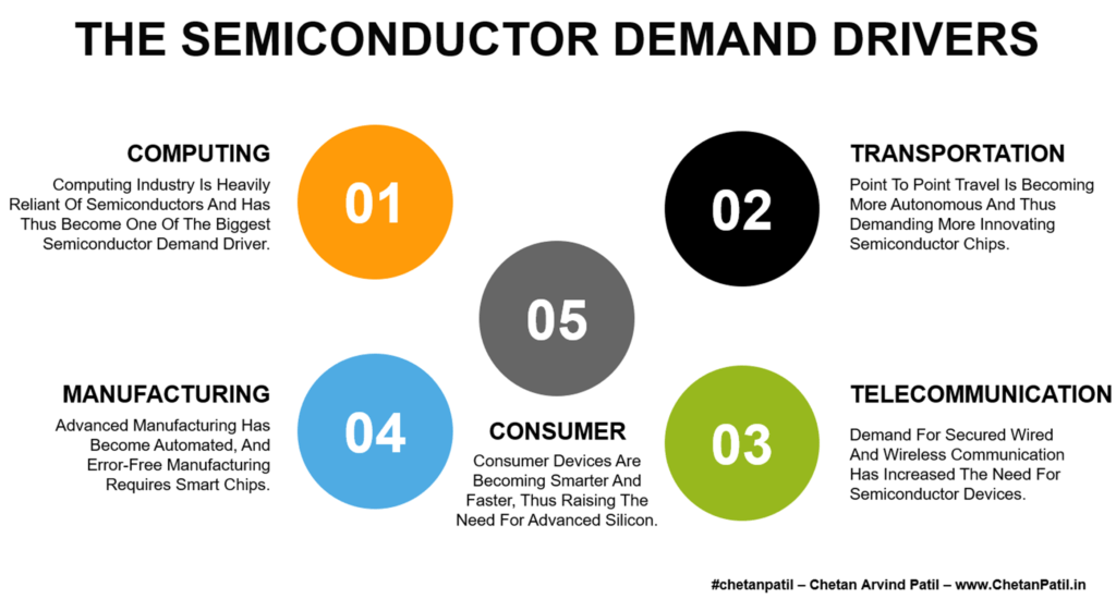
Computing: Computing industry is by far the most semiconductor demand generating domain. From laptops to servers, semiconductor products are powering all day-to-day life. As the data workload has become more complex, the need for advanced computer chips has increased. Hence, computing has become a critical demand driver for the semiconductor industry.
Transportation: From aircraft to trains to metros to automotive, everything is becoming more automated and advanced. These industries are demanding new features that can provide safety and entertainment at the same time. It is where efficient semiconductor chips are required and therefore have become a vital demand driver for semiconductors.
Telecommunication: Both wired and wireless solutions are heavily dependent on semiconductors. As the need for secured high-speed connectivity has increased, the demand for novel semiconductor solutions has increased further. It makes telecommunication another big demand driver for the semiconductor industry.
These demand drivers are creating a new market, which often demands new features. These new features eventually mean that new and advanced semiconductor solutions are available. For example, a new wireless solution (6G) will demand secure chips to drive high-speed voice and data traffic. Such a new feature market creates new opportunities for the semiconductor industry, and every year new landmark technology are launched. Thus, ending up enabling more demand for semiconductors.
As the world becomes more hyper-connected and remote, these demand drivers will keep creating the markets for new semiconductor solutions. And, it will be important that both the academia and industry keeps investing heavily in the research aspect of the semiconductor. As it will be key in enabling new semiconductor solutions ahead of time.
Manufacturing: The manufacturing industry relies on automated solutions from robots to equipment. All these solutions require advanced chips that need to work without introducing an error. Such market is driving the semiconductor industry revenue to new levels.
Consumer:Consumer products like smartphones, gaming consoles, security solutions, appliances, and so on are all heavily equipped with semiconductor chips. The consumption of such solutions is increasing year on year, and thus makes consumer solutions another demand driver for the semiconductor industry.
Investing more in the research aspect will ensure that the semiconductor industry at large is prepared for the next-gen needs of the demand drivers. It is important to do so as the key demand drivers have to be presented with the next innovative solution ahead of time, and this requires different semiconductor companies to provide a robust technology roadmap that can provide a high-level of confidence. As the semiconductor industry grapples with Moore’s law and the More-Than-Moore debate, it will be crucial to focus on how the demand drivers evolve.
In the long term, companies that can articulate and deliver the right product at the right time to the right market will win continue to win the semiconductor race.
Moore’s second law, or Rock’s law, states that the cost of a semiconductor manufacturing plant doubles every four years. It is in line with the increase in transistor density, which demands high-tech and advanced solutions which directly contribute to the cost of semiconductor manufacturing plant setup.
As more countries around the globe gear up to attract new semiconductor manufacturing capacity, the investment component becomes the more crucial one and much more than the semiconductor technology itself. High investment involves risks, and to de-risk any future unknown issues, government support is often required. It is where incentives come into the picture and help push private players into building new FABs and OSATs.
How much it costs to build a FAB/OSAT:
MIN-FAB: ~$1 Billion+
MEGA-FAB: ~$4 Billion+
GIGA-FAB: ~$12 Billion+
OSAT: ~$100 Million+
Semiconductor technology and also semiconductor equipment decide the investment of next-gen semiconductor manufacturing plants. These two components together can increase the cost of a new facility significantly. High investment is also the primary reason to opt for the semiconductor technology that drives a faster break-even point.
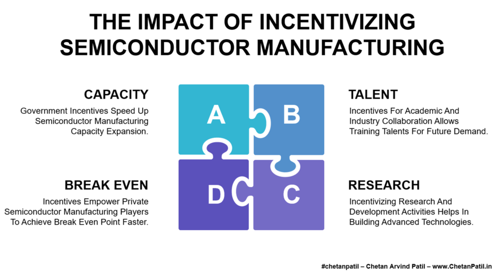
Capacity: Incentives at the central/federal and state-level helps the building of new (and/or upgrading old) semiconductor manufacturing. Private players can take advantage of the tax or other related benefits/incentives to drive other semiconductor manufacturing-related activities like expanding existing facilities to drive future demand or hiring more human resources.
Talent:Incentivizing semiconductor manufacturing empowers private players to hire more talents. In the long term, it also creates more job opportunities. Governments who provide an extensive incentive to universities for semiconductor research/education also encourage the training of high-tech talent. Countries like US and regions like Europe are two such examples apart from several Asian countries.
The race to set up new capacity at new/existing semiconductor ecosystem is heating up. The factor that attracts investment in a semiconductor manufacturing plant is the incentive. Over the last decade, governments of countries that have heavily incentivized semiconductor manufacturing have seen an exponential increase in semiconductor manufacturing capacity. Taiwan, South Korea, Japan, and China are a few such examples.
As more new semiconductor manufacturing regions come around the globe, governments must keep heavily incentivizing to drive next-gen semiconductor manufacturing infrastructure.
One of the most important long-term benefits of incentivizing semiconductor manufacturing is the long-term capacity building for the in-country requirement. Heavily depending on a high-tech solution like semiconductor is going to be a risk in the future.
By incentivizing semiconductor manufacturing, private players can foster the growth of building a semiconductor ecosystem. Doing so can make any given country self-reliant concerning the semiconductor supply chain.
Research: Incentives enable private players and universities to foster a research and development environment as companies/universities can divert the saved cost towards building the future advanced semiconductor logic to equipment.
Break Even:Incentives also reduce the CapEx, which helps in achieving the break even point faster. It also reduces the liability and mitigates the business-related risk.
The growing demand for semiconductor solutions in different day-to-day products is driving the need for new capacity. The only way to balance this capacity demand is by providing long-term incentives. To make the semiconductor FAB/OSAT a reality, a long-term strategic plan that balances the technical and business aspect is also required. It requires a handshake between the government and the private players.
Governments with attractive incentives will win the battle of building a new semiconductor manufacturing capacity. Doing so will also empower countries to take control of in-county semiconductor demand.
Countries all over the world are coming up with policies and incentives targeted towards semiconductor manufacturers. It is due to the dependence countries will have on semiconductors which are the backbone of the digital economy.
In the same line, India has also come up with several incentives to foster the semiconductor manufacturing ecosystem. However, incentives only help to a certain extent and beyond which laser-focused road map driven planning is required. The road map also empowers the potential investors and enables them to diversify investment as part of the long-term strategy.
When it comes to the semiconductor manufacturing road map, no one recipe fits all. India needs its India-specific road map for semiconductor manufacturing. India is already home to the majority of the top semiconductor design and research institutes. It makes the process of building semiconductor manufacturing slightly less complex but still requires a long-term strategy.
A road map can have several key components. However, if incorporated well, it can enable a steady and robust semiconductor manufacturing growth in India.
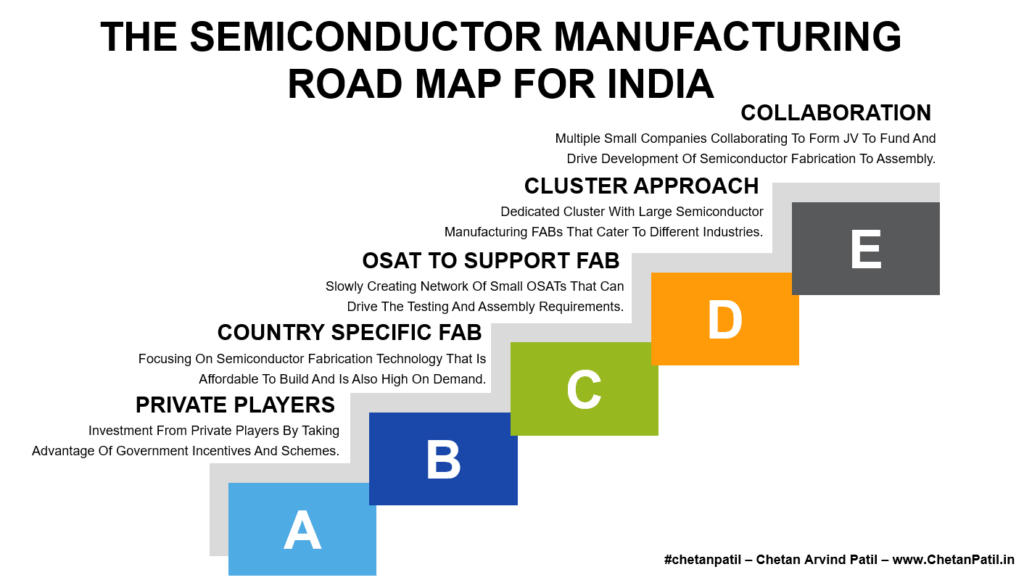
Private Players: Private players are critical in enabling semiconductor manufacturing. These private players often have to invest a large sum of money for a semiconductor manufacturing plant. There are already several incentives that the Indian government has launched. Now, India needs one top semiconductor manufacturer to take advantage of these schemes and thus slowly turn the plan into reality. Private entities should also actively engage with the government. It should provide a detailed overview of where the bottleneck lies and how government can help in filling these gaps.
Country Specific FAB:India has the market and demand for semiconductor products. Focusing on these requirements and then building the semiconductor FAB can enable India (private and government) to drive in-house requirements. It will also require the potential semiconductor manufacturers to focus on semiconductor technologies that fulfill the semiconductor demand for India. And, as a long-term strategy, it can also lay the foundation of future semiconductor technology for India and the world.
OSAT To Support FAB: Semiconductor FAB by itself does not make up the semiconductor manufacturing ecosystem. It requires a support system in the form of a supply chain, which also includes OSAT. OSAT is critical to enable packaged goods to the customer. India already has OSAT specific policies, and taking advantage of them to drive the support environment can bring an end-to-end semiconductor manufacturing ecosystem.
Cluster Approach: India is already home to top non-semiconductor manufacturing companies. These companies have been successfully catering to not only India’s demand but also exporting to different countries. Automotive is one such example. Over the decades, dedicated automotive regions have turned into giant clusters with end-to-end automotive-focused manufacturing needs. As India moves towards the next era of the wireless and digitally connected economy, similarly, semiconductor-focused cluster manufacturing is the need of the hour.
Collaboration:In the end, semiconductor manufacturing is all about long-term planning. Either with customers or with public bodies. All of the successful semiconductor manufacturing-focused clusters around the globe are actively collaborating and redefining their planning. They do so by actively engaging with the universities or with other private players. Such a long-term collaboration is key to driving next-gen innovation. India needs to have a collaborative environment to drive in-country semiconductor manufacturing. Several attempts have failed, and India certainly needs one such collaboration to kick off the semiconductor manufacturing story.
Successful and profitable semiconductor manufacturing region today started with one FAB or OSAT. Today, these regions are a big part of semiconductor manufacturing and are re-developing for the next century.
Without a medium to large-scale FAB/OSAT, India will stay dependent on its future semiconductor demands. It is about time that India embarks on the road map for the next decade. Otherwise, the gap between the semiconductor demand and semiconductor manufacturing in India will keep growing, and India will be more dependent than ever.
Year on year, for decades, Moore’s law has inspired semiconductor designers and manufacturers to pack more devices in the same silicon area. It has thus provided the computing world with different types of semiconductor products to process the data as per the power-performance goals.
One semiconductor product that has benefitted the most from Moore’s law is the XPU. XPU are of different types, and the widely known ones are CPU (Central Processing Units) and GPU (Graphical Processing Units). Apart from traditional XPUs, ASIC (Application Specific Integrated Circuits) have also enabled elegant computing solutions for decades.
ASICs are also of different types, and the most advanced ASIC is the FPGA (Field-Programmable Gate Array). FPGA is not new to the semiconductor market and has played a crucial role in industry and academia. One of the advantages of FPGA is the ability to get programmed/configured to prove-in different methods and that too after manufacturing. It has thus enabled several industrial applications from audio processing to wireless communication to rovers on Mars.
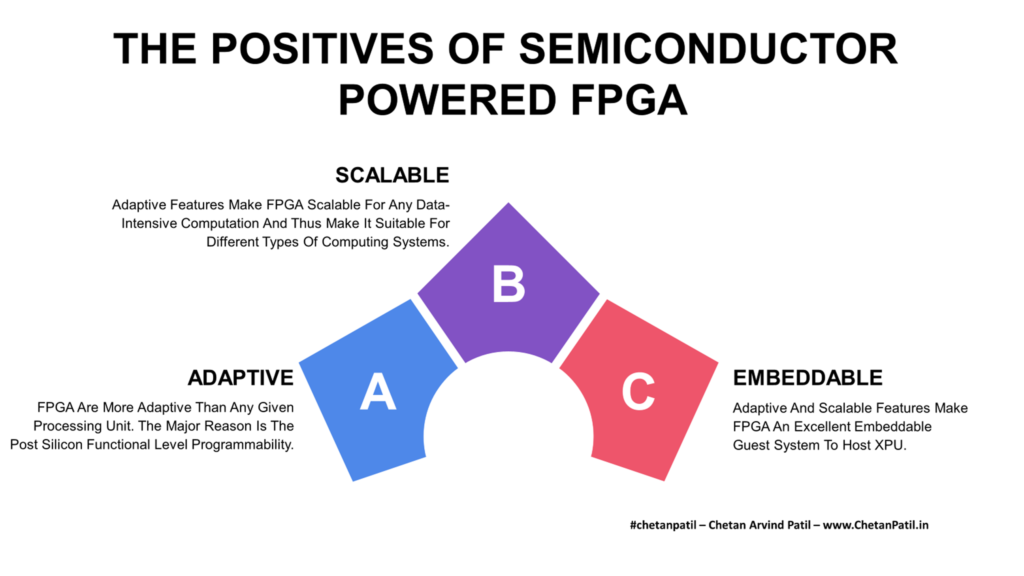
Adaptive: The design features of FPGA make it highly adaptive, and this provides the ability to deploy FPGA as per the target application requirements. It is possible due to the array of programmable blocks, which empowers developers to use (and also enhance) the FPGA as per the target application requirement.
Scalable: FPGA comes equipped with silicon features that enable them to be more scalable. Such features make them more adaptive than any traditional XPU. Such reconfigurability ability is possible due to the extensive libraries and IPs that the FPGA ecosystem has.
Embeddable:Several advanced computing systems often require dedicated ASIC that can take over the specialized task. This ASIC is often embeddable and comes equipped with the XPU system. In the same line, FPGAs are also embeddable and often carry out the specialized task on behave of the host system. FPGA being configurable are thus becoming a de-factor for the data learning world.
FPGA’s importance is growing further due to the adaptive/programming features that make it a perfect silicon for training a large amount of data on the go. ML/AI/DL is another area where FPGA has found a growing use. It is also one of the reasons why both Intel and AMD have invested billions of dollars to acquire FPGA-focused assets. These assets have enabled Intel and AMD to drive next-gen XPUs with embedded FPGA for specific post-manufacturing programmable requirements. Example applications can range from neuromorphic computing to inference-based processing to real-time metaverse.
Today, the FPGA market is approximately ten billion dollars. With the demand for real-time adaptive silicon increasing, the FPGA market will grow further and thus presents opportunities for both established and emerging XPU focused semiconductor companies.
The features of FPGA do not make it an alternative for traditional XPUs. One of the fundamental reasons for the fast growth of XPUs like CPU and GPU is the ease of use, and this is something that is not possible with FPGA due to the target application and the design/IP complexity.
However, in the last couple of years, the story has changed. Today, performance-oriented XPU comes equipped with FPGA (embeddable-FPGA or eFPGA). One important reason is to allow training/testing of learning algorithm on the device itself. Such silicon features are going to form the base for advanced X-Reality products.
Like any other computing system, FPGAs also have drawbacks. The majority of these drawbacks are not going to stop the growing FPGA market. However, overcoming these fundamental challenges can speed up the deployment of FPGA on critical infrastructure.
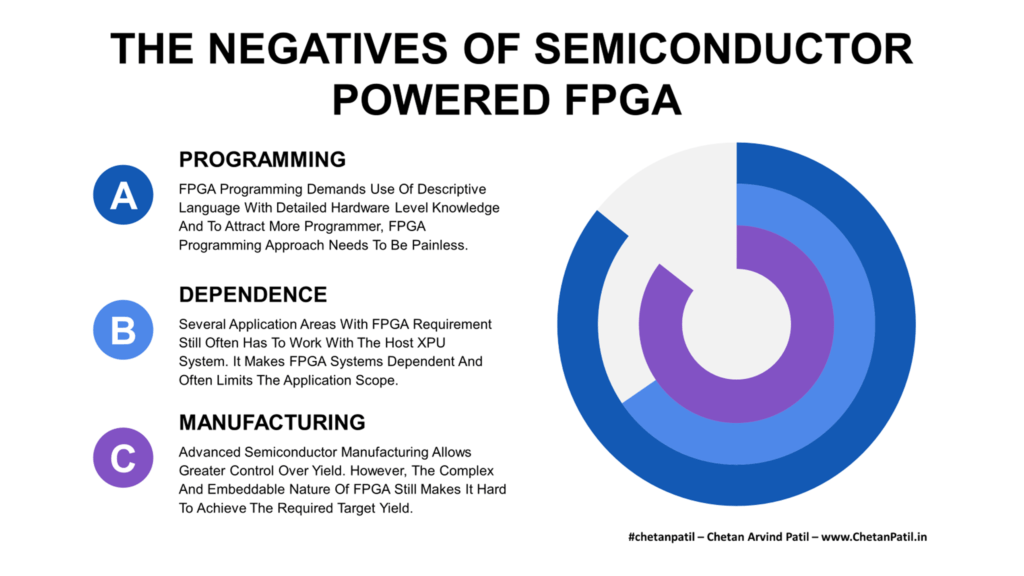
Programming: Programming FPGA is not easy and demands detailed in-architecture understanding. Companies developing FPGA often provide a set of software libraries and tools to make the programming experience easier. However, for the FPGA to become an attractive platform, the programming language needs to evolve. It might enable faster algorithm development to drive cost-effective solutions.
Dependence: There are several application areas where FPGA cannot get deployed without a host system. It makes them dependent on the host XPUs. FPGA developers have tackled this issue by utilizing low-power SoC, but the cost and complexity it comes with are high.
Manufacturing:FPGA is very complex, and embedding them with any other XPU makes the manufacturing process harder. Semiconductor manufacturing has advanced a lot, but driving high yield is still a big challenge for advanced nodes with highly complex designs like SoC FPGA. As FPGA becomes part of a more complex computing system, the manufacturing methodology will have to evolve too.
Neural Processing Units (NPU) are becoming a given feature for every new XPU. Intel, AMD, Apple, Microsoft, Qualcomm, NVIDIA, and several other companies are increasingly adapting their XPU to have NPU blocks. The building block of NPU is still FPGAs, and this makes it critical to overcome all the FPGA-related challenges to ensure the users can make the most of the FPGA ecosystem and are driving the adoption at a faster rate.
The semiconductor giants have already acquired long-term assets to make their XPUs FPGA friendly. These semiconductor companies are already delivering FPGA-inspired solutions and are pushing the computing industry to the next level. It showcases that FPGA will keep growing, and the semiconductor industry will keep coming up with advanced FPGA silicon.
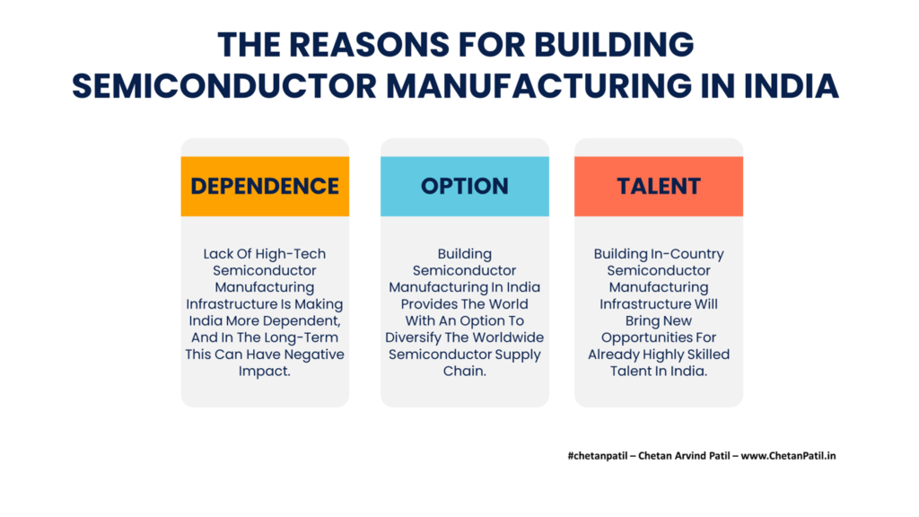
THE REASONS FOR BUILDING SEMICONDUCTOR MANUFACTURING IN INDIA
By 2025, India will be one of the top electronics markets with an expected market size of over $500 Billion. The foundation of this market will be laid by the building blocks of electronics products: the semiconductor chips. However, to cater to such a large market, it is critical to develop an in-country semiconductor manufacturing ecosystem, something India lacks.
India is already home to all the top semiconductor design houses, still does not have large-scale FAB or OSAT manufacturing facilities. For decades, there has been a push to attract investment to build a semiconductor manufacturing ecosystem in India. However, none of the efforts have materialized. On top of all this, year on year, the cost of building a semiconductor manufacturing facility is increasing, and further delay is only going to put the plans to bring large-scale FAB/OSAT in India a distant dream.
Dependence: Growing electronics market demands more semiconductor products, which makes semiconductor manufacturing a critical component. India has already lost out on manufacturing drive semiconductor business and has created a heavy dependence on facilities located outside of India. A supply chain crunch thus can have a massive negative impact not only on the consumer electronics market but also on the exploding digital economy of India. All this makes in-country semiconductor manufacturing a must-have ecosystem.
Option: Investing in India and building FAB/OSAT provides another avenue to the worldwide semiconductor industry. It will also diversify the semiconductor supply chain. Given the recent geopolitics around semiconductors, India’s open market certainly presents as an attractive destination. And, this can also take away the growing dependence on specific regions/countries.
Talent: India is home to millions of skilled talent. Several of these are already part of the semiconductor industry. On another side, the younger population is heavily contributing to semiconductor-driven research. A semiconductor manufacturing ecosystem will empower skilled talents and provide them a platform to explore the other side of semiconductor product development. In the long run, it will only benefit the semiconductor industry at large.
The government of India for years has come up with several incentives and measures to attract investment to build an end-to-end semiconductor ecosystem. Some of these incentives have worked, and several of these have not. The ones that have not worked out are the critical ones (semiconductor FAB/OSAT). Thus, demanding a new approach to attract top players to kickstart a FAB/OSAT ecosystem in India.
The lack of semiconductor (chip level) manufacturing in India will increase its dependency on other countries (for semiconductor component-level manufacturing). To power the future electronics market in India, it is vital to start semiconductor manufacturing facilities today. For sure, it is easier said than done, and a combination of a few critical factors have so far stopped India from being home to large-scale FAB/OSAT facilities.
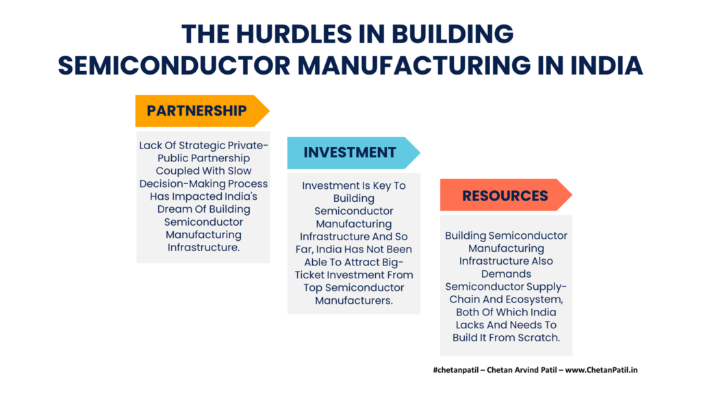
THE HURDLES IN BUILDING SEMICONDUCTOR MANUFACTURING IN INDIA
Semiconductor manufacturing is all about investment and technology. The technology part is easy to bring in as several of these processes are already available and often only require investment (facilities) to bring the product into reality. The critical part is the investment to build FAB/OSAT, and this is something India has not been successful in executing.
Attracting investment to build FAB/OSAT demands flawless planning and robust collaboration. India has several government-driven plans. However, execution at the ground level is still a distant dream due to the known and unknown hurdles.
Partnership: Semiconductor manufacturing is a sum game of two critical components: Investment and technology. Both of which require hand-holding from the government and also the private sector. All the successful (and underdevelopment) semiconductor clusters are based on a long-term private-public partnership. Such partnership has not happened in India (for semiconductor component manufacturing), and the lack of private-public venture is delaying the activities further.
Investment: In many cases, the government comes up with attractive incentives and policies (which India already has), and using them, private players start/grow their business. Even though there are several central/federal to state-level semiconductor manufacturing-focused inventive and policies, a step forward from the private sector has not happened. An investment push from the top semiconductor manufacturers can lay the foundation of semiconductor FAB/OSAT in India.
Resources: FAB/OSAT are big but not the only part of semiconductor manufacturing. There are several other support systems required to drive FAB/OSAT. It can range from raw materials to logistics to supply chain-related requirements. India has not focused on the end-to-end semiconductor supply chain yet and instead is focused more on the big players to set up FAB/OSAT. To ensure an end-to-end semiconductor manufacturing ecosystem develops in India, focusing on all (not a few) critical components is a must-have.
India has everything that a semiconductor manufacturing ecosystem demands: Talent, infrastructure, design companies, and research ecosystem. Still, business-oriented hurdles are stopping India from becoming the next big destination for semiconductor manufacturing. Thus, robust solutions around it are required (via public-private partnership).
The next few years will be critical in making a FAB/OSAT (thus building the semiconductor manufacturing ecosystem) a reality in India. If not executed correctly, it will put India’s growing electronics market heavily dependent on external factors.
The process of developing chiplets based silicon chips (mainly XPUs) demands new semiconductor design and manufacturing methods. These methods are not drastically different than what the semiconductor industry developed in the last few decades. Still, the product development steps have to adopt to ensure chiplets are a success in the long run.
These changes impact both the semiconductor design and manufacturing stages. Thus, both the design and manufacturing companies need to take a fresh look at how to approach chiplets inspired products so that all such products still meet industry standards without compromising on the quality,
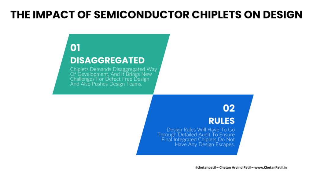
Disaggregated: Chiplets demand N number of chiplet to get designed individually, and during the post-manufacturing stage, this N chiplet needs to work together as a single system. It requires designers to simulate the chip at the die/chiplet level and then at the chiplets (as a single system) level. It is not a new process, but when it comes to complex chiplets inspired products (XPUs based on chiplets), there is a high risk of design escape.
Rules:At the individual die or chiplet level, design rules today are more robust than ever. Couple this with the designer’s experience, and the error rate goes to near-zero. However, chiplets will work if the integrated chiplet will. It makes the application of design rules at the chiplets level critical, and that too without any design rule escape. Simulation and verification certainly try to reduce such issues. In reality, there will be lessons learned when it comes to design rules escape at the chiplets level.
When it comes to semiconductor design, the fundamental approach that chiplets changes are the disaggregated way of designing the same chip that otherwise would have been a single design file. Another impact is the design rules that ensure there is never an escape, but that also requires a fresh outlook for chiplets way of designing.
Semiconductor design so far has been more about single-die design. With chiplets, the level of design complexity increases tenfold. However, the complexity and the impact of chiplets are not only limited to the semiconductor design. Semiconductor manufacturing also has to go through process-level changes to ensure that the manufacturing aspect of the chiplets does not become a show stopper in the long run.
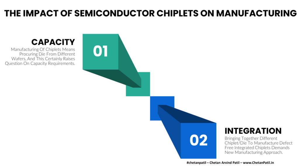
THE IMPACT OF SEMICONDUCTOR CHIPLETS ON MANUFACTURING
The impact of chiplets is also applicable to the semiconductor manufacturing aspect of semiconductor product development. The primary reason is again the disaggregated way of designing. In the end, chiplets are an integrated system, and making it work at the semiconductor manufacturing stage is more complex than it seems.
The two critical impacts of chiplets on semiconductor manufacturing are capacity handling and managing integration (assembly mostly). These two impacts also mean a new outlook towards supply chain management.
Capacity: Fabricating, assembling, and testing N number of chiplet to form a single chiplets does demand a new approach towards manufacturing capacity planning. The planners have to track and trace each and every chiplet that will become part of the chiplets. This may not have a very drastic impact on the capacity, but from the supply chain point of view, chiplets certainly bring a new level of complexity (and opportunity). Given the final part of the manufacturing occurs at the back end side (assembly/testing), error-free planning and traceability are required to capture any kind of manufacturing escapes.
Integration: Integrating several chiplet to create a single chiplets is not an easy task. On top, to ensure the manufactured chiplets meets industry standards, the semiconductor manufacturing companies have to create a new set of process that drives the fabrication and assembling of chiplets based products. As more semiconductor design companies opt for the chiplets process, the need for a new integrated manufacturing system will increase, and this demands semiconductor manufacturing companies to be ready ahead of time.
The race to provide solutions beyond Moore’s law demands new approaches. Chiplets is one such technology and requires a fresh outlook towards semiconductor design and manufacturing. As more semiconductor companies opt for chiplets and similar heterogeneous packaging solutions, the need to adapt the semiconductor design and manufacturing aspect will change.
In the end, chiplets will push the semiconductor industry towards a new era, and hopefully, the long-term impact is nothing but all positive.
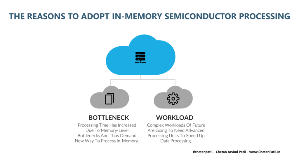
THE REASONS TO ADOPT IN-MEMORY SEMICONDUCTOR PROCESSING
Over the last decades, both industry and academia have spent numerous hours to enable different types of semiconductor design and manufacturing methodology to drive next-gen processing units. These processing units today power the computing world and often require billions of ever-shrinking structures.
As the data world moves towards more complex workloads coupled with the need for faster and real-time processing, the traditional processing units will not be enough for the computing task. To overcome challenges, the semiconductor industry (mainly companies focused on XPUs) is now adopting new semiconductor design and manufacturing methods for processing units. Chiplets is one such example.
In-Memory Processing Combines The Memory Units And Processing Units Into One Single Block And Thus Enabling Faster
However, the problem chiplets solves is the technology-node wall, and thus enable the future demand of a more efficient system without compromising the shrinking transistor size. In the long run, chiplets may not solve the memory bottleneck, as it occurs due to the need to bring the data from the lower level memory to memory closer to the processing units. All this leads to traffic and thus architecture-level bottlenecks.
Bottleneck: The time required to bring the data from lower-level memory to high-level memory (closer to the processing units) adds a time-related penalty and leads to a bottleneck when a given XPU has many processing units. Memory and compute level bottlenecks are thus demanding new processing solutions, and in-memory processing could be one such solution.
Workload: Workloads today demand video to audio to text to graphics-related processing. Traditional XPU design can handle these but again require different dedicated processing units for specific processing requests. NPU for neural, CPU for computing, DSP for digital, and so on. Specific purpose processing units add complexity. Thus, an in-memory processing unit solution can provide a foundation to minimize the block-level complexity and thus enable faster workload processing by bringing computing to the core of memory units.
Designing and fabricating different computing units can unlock new features that can speed up the computing world for future workloads. There are several challenges and hurdles in bringing this to reality. However, if done correctly, then the impact is only positive. In the long run and how the computing world is changing year on year, In-Memory processing is a path forward for data-heavy systems like server-grade XPUs.
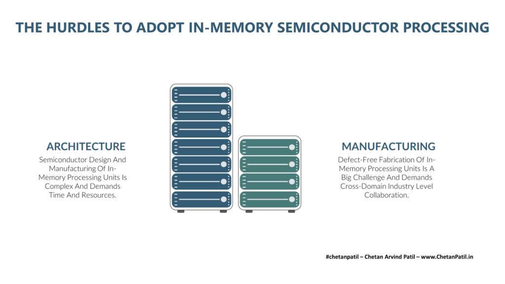
THE HURDLES TO ADOPT IN-MEMORY SEMICONDUCTOR PROCESSING
In-Memory processing units are a promising solution to tackle both the XPU bottleneck and the demand to handle complex workloads. Both academia and industry have proposed several solutions with many in-memory processing units ideas already tried and tested.
However, using in-memory processing units at the server level (where this solution finds the perfect fit) is still a far distant dream. The two critical hurdles stopping the large-scale adoption of in-memory processing units, and both of these go hand in hand.
Architecture: Combining processing units and memory units into a single unit (manufactured together) demands thorough research and design. It takes resources, cost, and time to do so before a viable product gets released. While it is not impossible to come up with a working mass-market in-memory processing unit solution, the time taken and risk involved is too high, something only a selected few companies in the market are capable of doing so.
Manufacturing:After semiconductor design, the semiconductor manufacturing stage is critical in fabricating two different units into one. In-Memory processing units demand combining two separate semiconductor manufacturing worlds. Doing so requires semiconductor design, semiconductor FAB, and also semiconductor equipment manufacturers to come together.
XPUs for the throughput-oriented requirement will keep evolving. Yesterday it was CPU and GPU, today ASIC/FPGA, and tomorrow it could be In-Memory processing units. In the end, as long as the solution is feasible from both the design and manufacturing point of view, the market will embrace it.
Several emerging companies are already coming up with new architectures to design next-gen XPUs. In-Memory processing units will also go similar traction, and it will be interesting to see how the market will behave.
THE COMPLEXITY OF SINGLE-TECHNOLOGY-NODE ARCHITECTURE
To ensure high-speed processing, one active component in a computer system – the Central Processing Unit (CPU) – has seen numerous technological advancements.
The CPU advancements have been distributed equally on the design and the manufacturing aspect of the semiconductor development process, both driven by Moore’s law.
Design: During the pre-internet era, the CPU used to get designed to handle basic input/output tasks. For such requirements, the data and memory handling were not complicated as it is today, and a single-core/unit of CPU could do the required task. As the world moved towards the digitization brought forward by the post-internet era, the multi-processing solution came to use. The next decade or two saw innovative CPU designs alongside the active components like GPU, Memory, Interconnect, ASIC, and FPGA.
Manufacturing: In 1990, the Intel P5 Pentium used an 800 nm technology-node, and in 2021, Intel is planning to move towards a third-generation of 10 nm with its Alder Lake series of microprocessors. Intel’s competitor AMD has already taken the lead with its 7 nm technology-node. Mobile and smart domains are already using a 5 nm technology-node and marching towards 3 nm.
The exploding data-intensive, compute-intensive and memory-intensive computation is now pushing the world from the general-purpose to specific-purpose computer architectures.
However, the foundation for a specific-purpose architecture was laid long back by System-On-A-Chip (SoC). SoC is an integrated chip that incorporates not only CPU but also other active components like the GPU, Wireless Chips (Cellular/Wi-Fi/Bluetooth/GPS/NFC), Memory, ASIC (Different types of XPU), and in some cases combined with FPGA to form SoC-FPGA.
SoC is vital for mobile devices and solutions where there is not much room to take advantage of the form factor. For a data center, there is the possibility to split out the GPU (and other XPU) as a co-processor (huge is size) with its power and cooling techniques. However, the same is not feasible for a mobile device like a smartphone or any IoT device.
Semiconductor Manufacturing Will Hit Technology-Node-Wall, Driving The Need For Multi-Technology-Node Architecture
On top of this, every block inside the SoC is fabricated using the same technology-node. This brings design and manufacturing complexity as the transistor size keeps shrinking. The design to fabrication to testing to packaging challenges added due to new technology-nodes eventually adds costs, apart from the cycle time required to prove the working of the new products with new generation of the technology-node.
To overcome cost and other technical challenges brought forward due to advanced technology-node, a new approach to design and fabricate the SoC’s internal blocks using different (new/lower and old/higher) technology-node needs to be explored. This design approach can be termed as Multi-Technology-Node Architecture.
What Is Multi-Technology-Node Architecture:
Design And Fabrication: Ability to design and fabricate active blocks inside the SoC with different technology-node. GPU can be at 14 nm while CPU is at 7 nm.
Technology-Node: The transistor size within each block follows a specific technology-node. Different blocks can use different technology-node.
Interface And interconnect: Packaging the blocks with different technology-node separately and sticking together with the help of a high-speed interface and interconnect.
Memory: Unified high-speed and high-bandwidth memory with its own technology-node to enable faster data flow.
Testing: Each block of SoC fabricated with a different technology-node can be tested separately before packaging.
Packaging: Follows System-In-Package (SiP) and other related heterogeneous packaging processes to stitch the all blocks of SoC fabricated using different technology-node.
The major advantage of Multi-Technology-Node Architecture will be the ability to balance the cost and cycle time.
The cost of fabricating some components as a separate die with high technology-node (more than 14 nm) and then packaging it to alongside blocks using advanced technology-node (7 nm or less) has the potential to lower the cost of fabrication and manufacturing. It also means the blocks of SoC can be fabricated at a different location and then packaged at the OSAT for validation, thus lowering the cycle time to market due to parallel fabrication.
Multi-Technology-Node Architecture will also drive IP based SoC block-level solutions that can bring more innovation in the SoC semiconductor space.
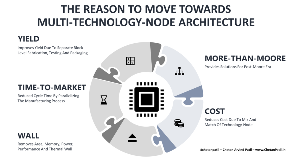
THE REASON TO MOVE TOWARDS MULTI-TECHOLOGY-NODE ARCHITECTURE
There are numerous reasons (and benefits) as to why computer architecture design and manufacturing should move towards multi-technology-node architecture:
Yield: Putting so many blocks together inside an SoC using a single-technology-node architecture design (Example: 7 nm technology-node) brings complexity. It puts constraints not only on the fabrication side but also on testing and packaging. The high-yield for every wafer fabricated with the SoC becomes a difficult task. The electrical testing itself needs to be detailed to ensure that the blocks are working as per the specifications. This complexity quadruples at advanced technology-node like 5 nm and lower. Using multi-technology-node architecture ensures that the different blocks are designed and fabricated with different technology-node. All the higher technology-node (more than 14 nm) are already proven in the market, and this speeds up the fabricating to testing processes. It also massively helps eliminate waste and improves the yield.
Time-To-Market: Proving out the solution at a specific advanced technology-node (using single-technology-node architecture) takes time with numerous SOC components that need to be carefully designed and fabricated in a single die. Any issue with the design or manufacturing eventually increases the time taken to launch the product in the market. Given how stiff the competition is in the semiconductor industry, any delay can cause loss and market position. With multi-technology-node architecture, only specific blocks using new technology-node needs to be more focused on to ensure correctness. The rest of the blocks can take advantage of higher technology-node that have been in use in the market for years and have proven semiconductor process/product.
Wall: The SoC is designed mainly for mobility. Even today, there is no way to provide unlimited direct power to the devices using the SoC in a mobile scenario. Eventually, one has to rely on battery technology to bring mobility. However, fabricating components with thousands of transistors consume power, and improving performance-per-watt (PPW) is becoming a challenge. The SoC design will soon run into area, memory, power, performance, and thermal wall with single-technology-node architecture. Multi-technology-node architecture can provide avenues to bring new ways to manage thermal constraints (using innovative IP from different semiconductor companies) apart from lowering power consumption due to the no area constraints/requirements and also the usage of different types of technology-nodes.
Cost: Shrinking transistor size means adding more manufacturing capacity. The Pure-Play Foundry and IDM have to keep investing in new equipment and process recipes to ensure that the next technology-node is available within two years for any new technology-node launch. All this puts a lot of CapEx pressure on the manufacturing aspect of the SoC using single-technology-node architecture. Apart from manufacturing, the design houses (FAB-LESS/IDM) also have to keep investing in new R&D activities to bring innovation in transistor/device design to enable advanced technology-node process development. With multi-technology-node architecture, existing manufacturing capacity can be used efficiently.
More-Than-Moore: The semiconductor industry is trying to grappling for More-Than-Moore solutions. While there have been many designs for manufacturing processes that are catering to more-than-Moore solutions, multi-technology-node architecture is another approach that takes away the pressure of using the same-technology-node for every block of the SoC. Thus, giving way for another More-Than-Moore solution.
Apart from the above benefits, multi-technology-node architecture brings challenges too. It will require end-to-end semiconductor process validation before being used on a large scale.
THE BOTTLENECKS FOR MULTI-TECHOLOGY-NODE ARCHITECTURE
Multi-Technology-Node Architecture is not in use today. Few years down, it might be a possibility, and to ensure such architecture technique can be fabricated with the blocks of SoC using different technology-node, the following are the two bottlenecks:
Research And Development: Understanding the technical constraints of fabricating blocks of SoC using different technology-node requires research and development efforts. This is to ensure that there is no escape in the architectural process that leads to bigger issues than relying on a single-technology-node architecture way of designing SoC. A close three-way collaboration between Academia, FAB-LESS/IDM, and Pure-Play/IDM is required. Such collaboration requires time to show results. Hence, the research and development activities for multi-technology-node architecture should start today, not tomorrow.
Investment: Initial investment required to prove out the multi-technology-node architecture solutions is high. It requires investing in new software and hardware tools, in order to ensure that the SoC blocks fabricated separately can work in harmony and there are no technical constraints about which technology-node a given blocks used. The semiconductor packaging solution to allow multi-technology-node architecture integration will also be costly due to low scale usage.
As the semiconductor design and manufacturing companies start looking into the possibility of a multi-technology-node architecture, there might be more technical to non-technical bottlenecks apart from the above two.
In any case, multi-technology-node architecture has the potential to provide Post-SoC era computer architectures.