Photo by Maxence Pira on Unsplash
THE IMPACT OF WAFER SIZE ON SEMICONDUCTOR INDUSTRY
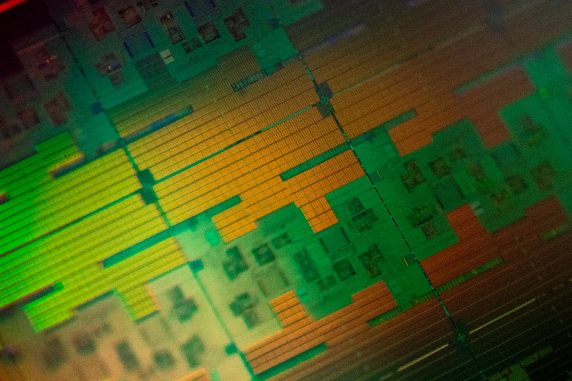
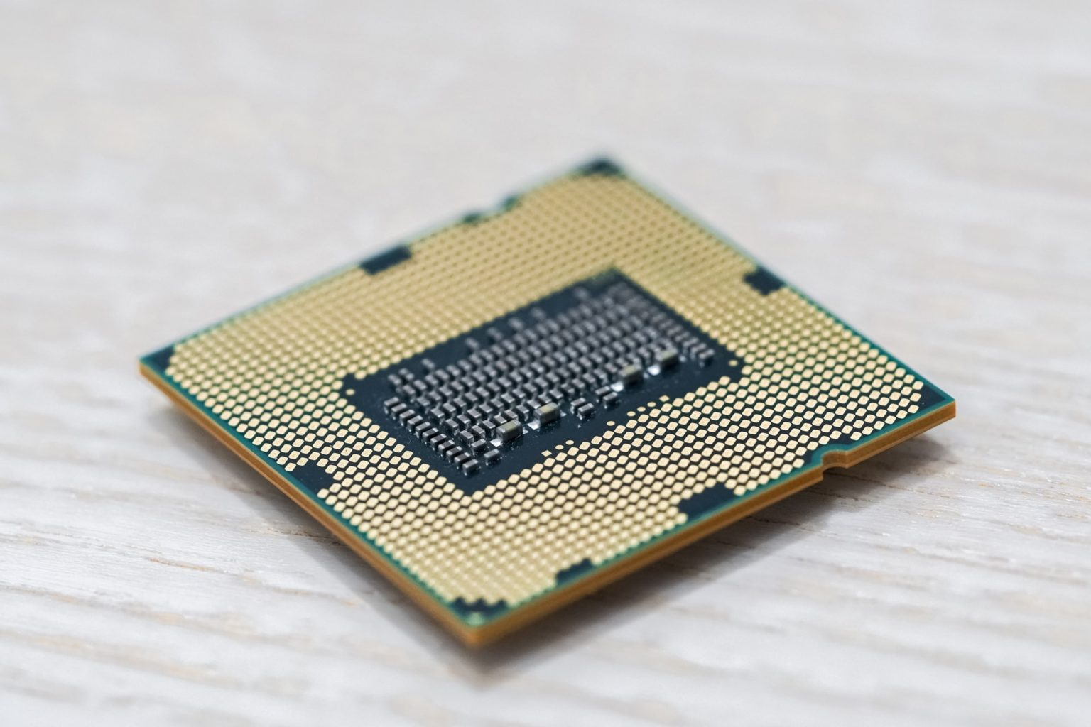
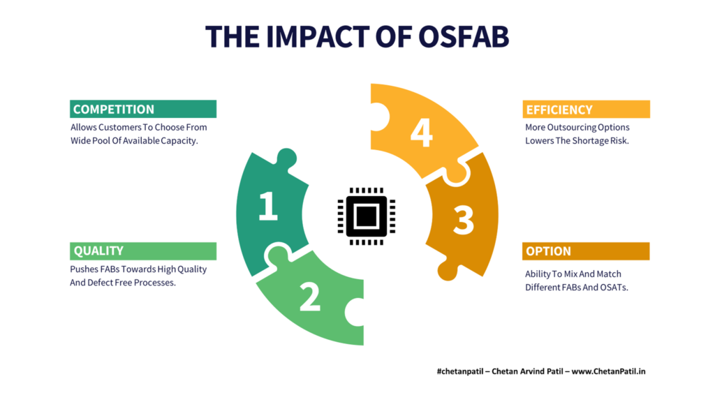
The semiconductor industry is built on the platform laid by silicon wafers that form the base of fabricating different types of advanced semiconductor products. The silicon wafers have gone through an incremental change in size/diameter over the last half-century. The growing need for advanced semiconductor products is now raising another round of discussion to move beyond wafer size in use today, mainly as a factor to improve the production rate of new semiconductor FABs and OSATs.
The semiconductor manufacturing facilities around the globe are categorized based on the wafer size they can handle. The majority of the FABs and OSATs today are focused on 200 mm (7.9/8 inch) wafers with a few focusing on 300 mm (11.8/12 inch). On other hand, only small FABs and OSATs cater to 150 mm (5.9/6 inch) wafers.
Wafer size plays a crucial role in deciding how the FABs and OSATs are built. The major reason is the equipment and tools that are required vary based on the wafer size and with the increase in wafer size the cost of setting up new FABs and OSATs increases too. This is why selecting the right wafer size a crucial.
Eventually, the choice of wafer size is more investment and strategically driven rather than technical. The reason for this is the impact of any change in wafer size on the full end-to-end semiconductor flow.
Wafer Size: Larger wafer size certainly provides more die per unit area. The extra area to fabricate more die eventually allows FABs and OSATs to fabricate and test/assemble more dies in a given time. This pushes the rate at which new products can be fabricated/assembled and to some extent increasing wafer size can also have a positive impact on the supply chain.
Die Per Wafer: Wafer size clearly defines how many die per wafer there will be. This allows the semiconductor design houses to gauge how much cost savings will be there. In the end, a smaller wafer for a high demanding product will lead to more wafer orders compared to a relatively larger size wafer. This balancing act is the major reason why companies often have to spend more time analyzing the pros and costs of selecting wafers from the business perspective.
Cost: Wafer size certainly dominates the cost of developing a semiconductor product. Apart from the cost of the wafer itself, there are FAB and OSAT costs that also need to be considered. Using a 200 mm (7.9/8 inch) wafer will certainly have a lower cost of fabricating and assembling semiconductor chips compared to a 300 mm (11.8/12 inch) wafer. In the end, it is all about creating the margin by selecting the right wafer size.
Yield: Historically, as the wafer size has increased the yield has come down. A product fabricated on a 300 mm (11.8/12 inch) wafer will have a lower yield compared to the same product on a 200 mm (7.9/8 inch) wafer. In the end, the final yield will be comparable, but the loss of yield as the wafer increases is mainly due to the time required to perfect the semiconductor process, which improves as more products use the same wafer size as the learnings can be captured and applied to improve overall product yield. Wafer handling also plays a crucial role in deciding the final yield and as the wafer size increases, it becomes difficult to lower the number of process steps due to a large number of die per given area.
Process: Wafer size is so crucial that semiconductor manufacturing facilities have to play a very long game and decide upfront the wafer size they will support over the next 5 to 10 years. The major factor is the cost associated with the process that is required to set up based on any upgrade in wafer size. To play safe, the majority of the semiconductor facilities have zeroed on to 200 mm (7.9/8 inch) wafer as they allow the balance of both the technical and business aspect. However, the need for 300 mm (11.8/12 inch) is putting pressure on FABs and OSATs to go for upgrades.
The above points clearly show the impact wafer size has on a different aspect of the semiconductor process. From cost to yield, there are several things to consider when the time comes to decide on which wafer size will be used to produce the next-gen product.
In the end, the decision is taken by the semiconductor houses who design and own the chip as the manufacturing facilities are only providing services.


THE STEPS TOWARDS NEW WAFER SIZE FOR SEMICONDUCTOR INDUSTRY
The current saga of semiconductor shortage is also raising the question of going a setup further and reigniting the discussion of going for the largest wafer size (300 mm (11.8/12 inch)) in production today.
This means pushing all the to-be-designed FABs/OSATs capacity to opt for 300 mm (11.8/12 inch) or even 450 mm (17.7/18 inch), which has not been used for full fledge production so far. The major argument is to increase the capacity per FAB/OSAT by equipping them with the process to churn more die per unit area. This will certainly require huge investment and not many FAB/OSAT will be willing to opt for anything more than a 200 mm (7.9/8 inch) wafer.
However, the semiconductor industry should also take a look at the wafer size from the growing dependency on semiconductor products. The most efficient way to eliminate any future demand that leads to the shortage is not only to build more FABs/OSATs but to also equip these facilities for future needs.
Even if the FABs/OSATs are initially designed and equipped with a 200 mm (7.9/8 inch) or 300 mm (11.8/12 inch) wafer, they should also start planning for 450 mm (17.7/18 inch) today. Following such a strategy will allow FABs/OSATs to be ready for the future demand that can certainly exceed the total capacity that will be available in the near term.
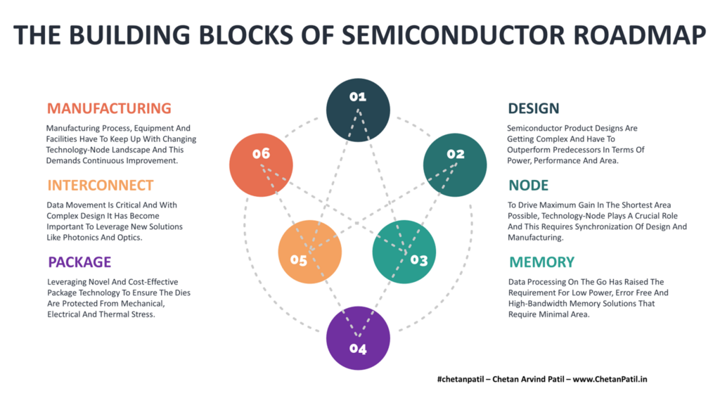
There are robust steps required to drive the adoption of a much larger (mainly 450 mm (17.7/18 inch)) wafer size than that is produced today, and the below roadmap provides a holistic view of why different steps should be taken towards larger wafer size.
Capacity: Today’s capacity is built on top of different wafer sizes and certainly it is not enough as per the semiconductor shortage. Building more FABs/OSATs will certainly provide higher capacity but not as much when the wafer size is increased. The semiconductor manufacturing houses need to take a long-term look at what is the loss of not upgrading to higher wafer size. It can start with 300 mm (11.8/12 inch) wafer FABs/OSATs and then move towards 450 mm (17.7/18 inch).
Collaboration: Setting up FABs/OSATs that can handle larger wafer sizes is costly. The only way to mitigate this cost is to bring different manufacturers together and invest in cluster-based facilities that cater to different customers. This will certainly invite IP and other confidentially issues but without a collaborative approach, it is not possible to increase capacity that is focused on larger wafer (300 mm (11.8/12 inch) or 450 mm (17.7/18 inch)) size.
FAB-LITE: Another approach towards handling wafer size can be to create a few niche semiconductor FABs and OSATs that only cater to future large wafer sizes. These can be facilities that are focused on 450 mm (17.7/18 inch) or 675 mm (26.6/27 inch) wafer FABs/OSATs. This strategy will make these new facilities the future R&D places that can drive the development of larger wafer size and as the technology progresses the lower cost of utilizing these larger wafer size will lead to mass production.
Target Node: Larger wafer size can also be used for specific technology-nodes. This way the cost of production can also be balanced along with the investment required. The best suitable nodes can be older nodes that have a more robust process than the future new technology-nodes. This can certainly help drive the adoption of higher wafer size too.
Efficiency: In the end, larger wafer sizes bring efficiency by shipping more parts in the same amount of time. The overall cost and investment will balance (as long as the production technology is affordable) out. This is another reason why the semiconductor industry should move towards a larger wafer size.
The steps if taken strategically can re-ignite the discussion of bringing 450 mm (17.7/18 inch) wafer into production and can certainly create a niche network of FABs and OSATs that can ramp up the production by providing more die per area (not just wafer but also facility area).
The semiconductor industry has to capture the cost of creating hundreds of FABs/OSATs versus a handful of high capacity FABs/OSATs that can handle much larger wafer sizes than today and thus providing a way to balance the cost and capacity for future demands.