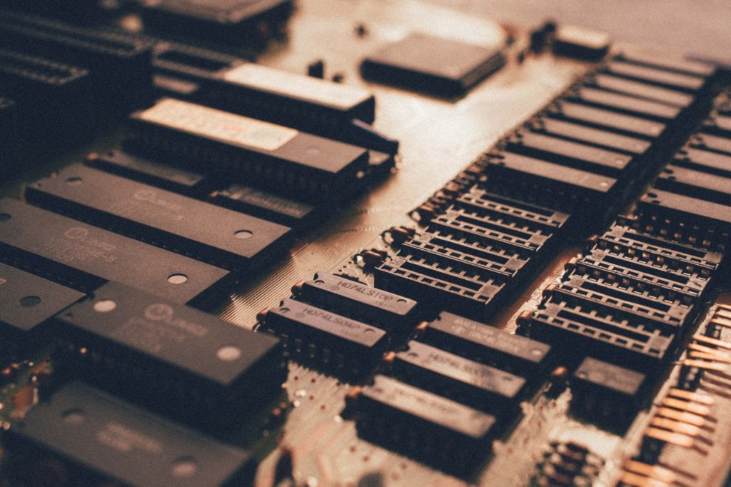
Photo by Mathew Schwartz on Unsplash
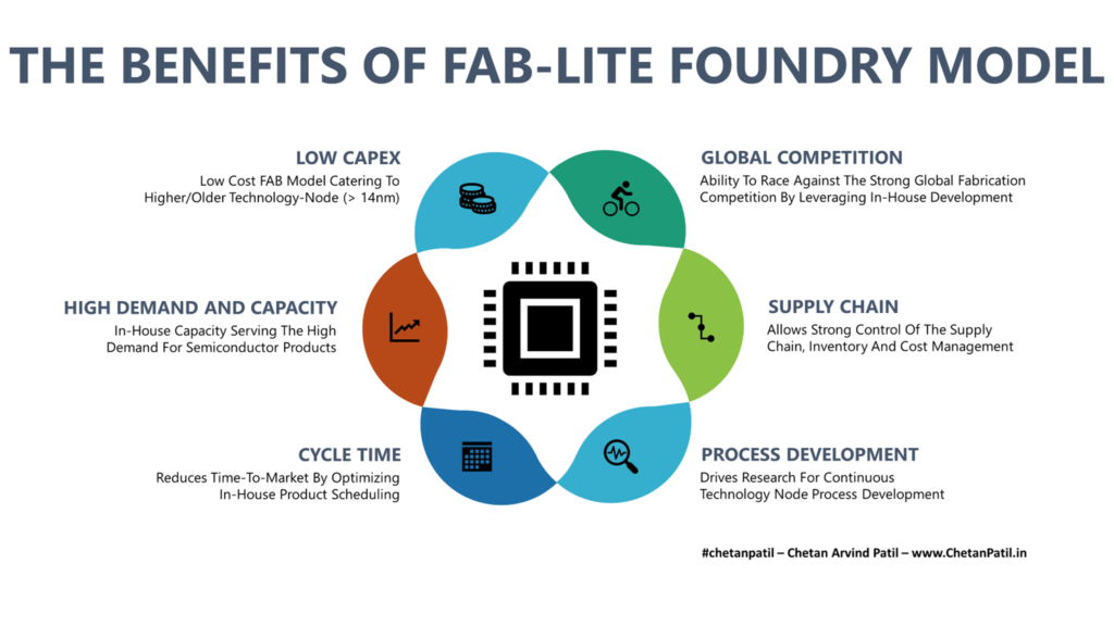
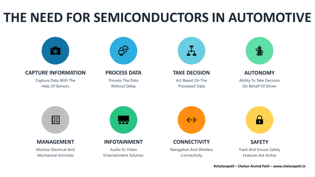
THE IMPACT OF SEMICONDUCTOR ROOT CAUSE ANALYSIS
Delivering high-grade products is the ultimate goal of every manufacturer. To do so, different industry-specific standards and processes are used. The same applies to the semiconductor manufacturing industry.
In semiconductors, as the technology-node shrinks, the cost to manufacture tiny silicon increases too. To ensure there is no waste of materials, time, and cost, several different strategies are deployed to screen the part before it moves ahead in the fabrication/manufacturing line.
One such strategy is root cause analysis. It so often happens, that the product being developed might encounter an issue during the qualification, testing, or packaging stage. Does not matter where the failure occurs, it is critical to understand the root cause. For an industry like semiconductor manufacturing, where every failing part can jeopardize not only the product quality itself but also the system to which it will eventually get glued in to. Such a scenario can certainly lead to millions of dollars in losses apart from a negative business reputation.
This is why holding on to every failing product and carrying out detailed root cause analysis is one of the major pillars of the semiconductor industry.
Over the last few decades, as the devices are getting tinier than ever, the importance of root cause analysis is growing due to the several impacts it has on the product:
Cost: Finding the root cause of why the product failed, empowers the team with data points to take necessary actions. It so often happens that the root cause analysis is more about setup or lab where the qualification or testing is being carried out and has nothing to do with the product itself. All root cause analysis and actions eventually can save cost by eliminating the need to re-do either the design or the qualification. Root cause analysis of failing products also ensures that the product will not fail in the field, thus saving years of investment.
TTM: Given the stiff competition in the semiconductor industry, the ultimate goal of every design and manufacturing house is to ensure that the product is launched within the planned time frame. In case of failures, root cause analysis provides a way to capture any severe design or process issue early on. This allows course correction to ensure the product still makes it to the market in time.
Quality: Qualification is an important process before the product gets released for production. Root cause analysis of any failing product during the development stage ensures that the product meets the high-quality industry standards. The standards increase as per the target domain and so does the importance of root cause analysis of the failing product/part.
DPPM/DPPB: Defective Parts Per Million/Billion is an industry-standard metric. The goal of semiconductor manufacturing is to lower DPPM/DPPB. In case of field failures, root cause analysis comes in handy, as it ensures the severe fails are captured to lower the DPPM/DPPB further. More so, when the product/part will be used for critical applications like automotive or wireless communications.
Root cause analysis has a major impact on semiconductor manufacturing. With new FETs and equipment launching every year, the role played by analyzing any smaller to big product-related failure is vital for both FAB and FAB-LESS companies.

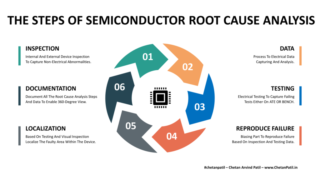
THE STEPS OF SEMICONDUCTOR ROOT CAUSE ANALYSIS
To capture the root cause that leads to the failure of a product, several steps are followed. Each of these steps plays a key role in providing data points to establish the root cause to drive defect-free manufacturing.
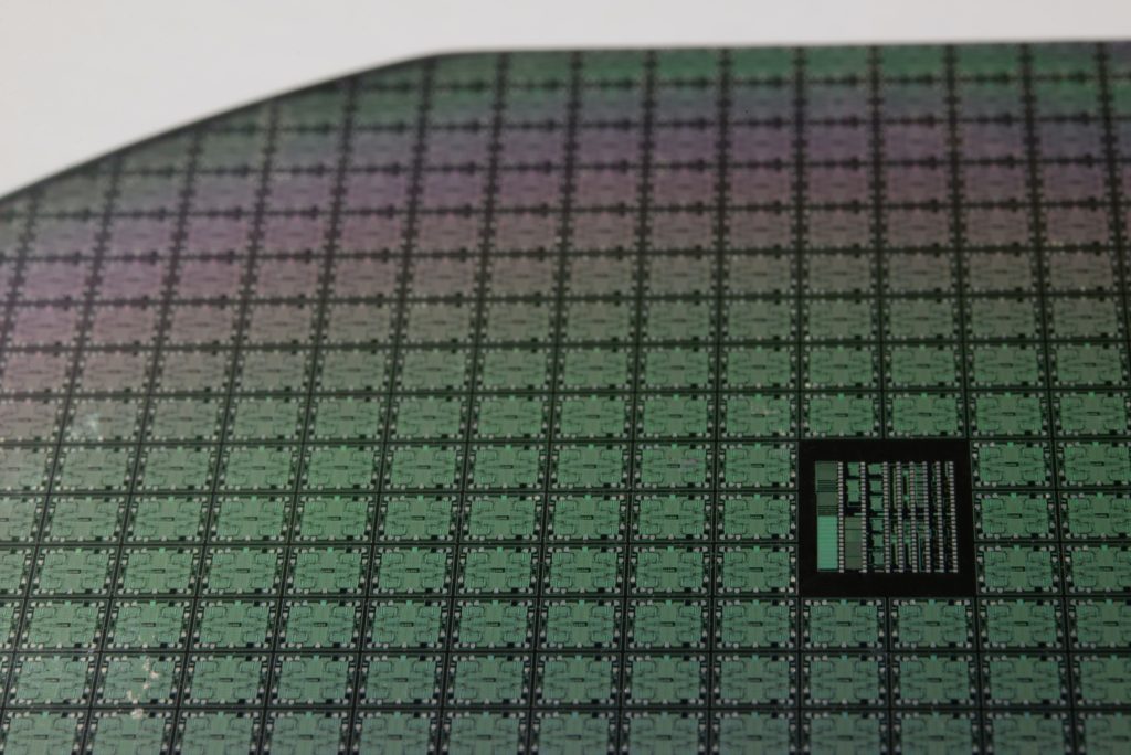
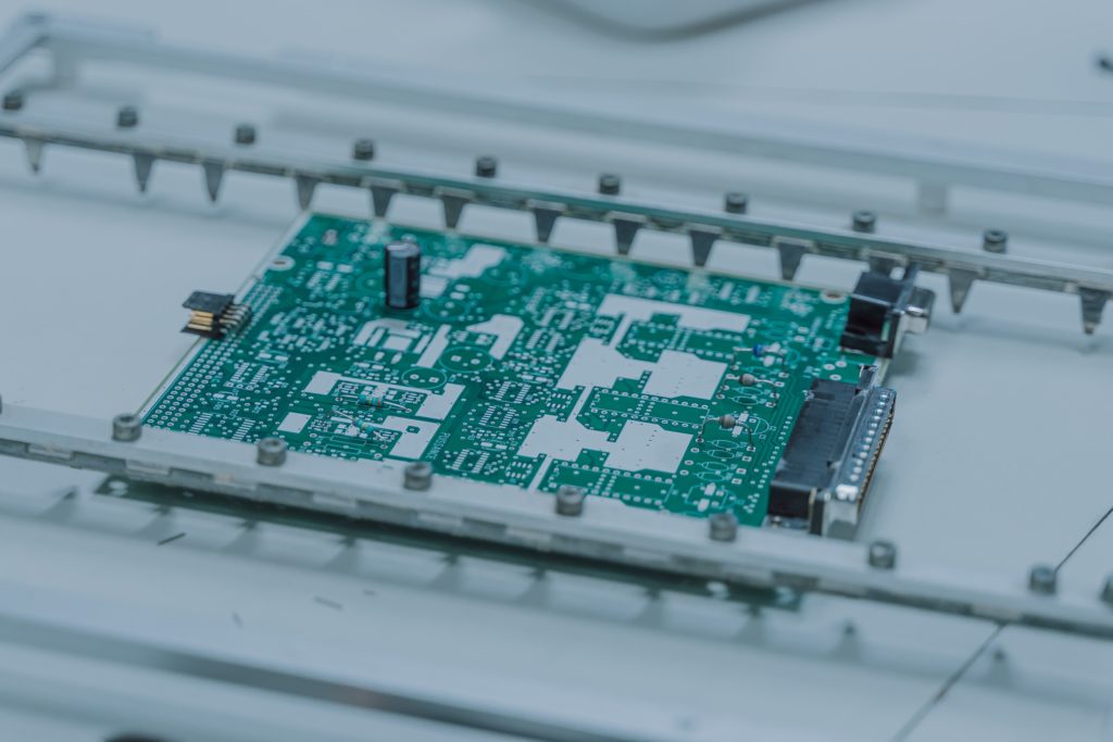
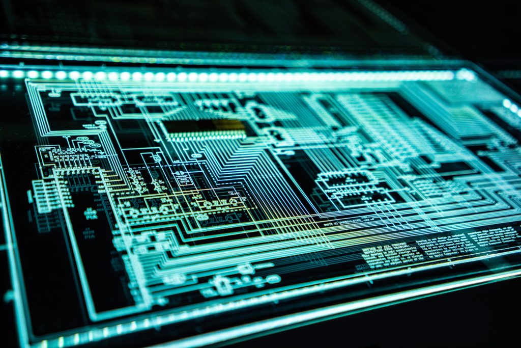
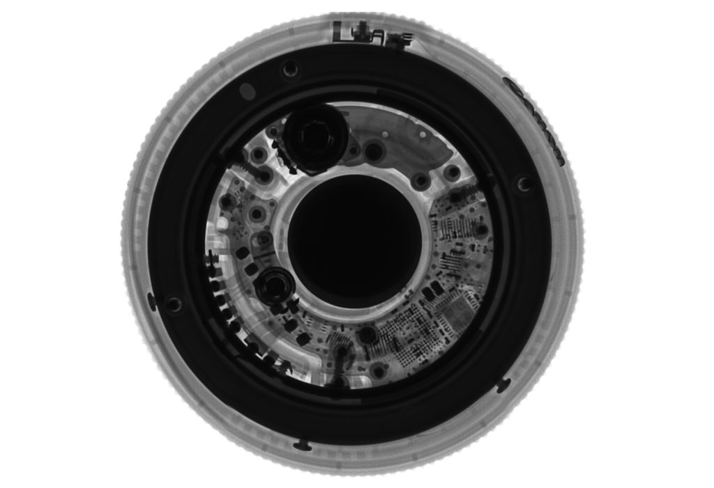
Inspection: Any given part/product that fails first and foremost has to go through a detailed inspection. Depending on the state of the product (whether in wafer or die or assembled packaged form), the inspection is performed. The images generated by these are then used to establish if any non-technical cause (handling, stress, recipe issue, etc.) leads to the failure of the product. X-Ray and SEM are widely used as these processes provide internal product details.
Data: The data points for the failing part/product come from different stages. All the parts have marking to trace their origin. As a starting point, the first data point is collected by testing the product without damaging it. Another data point can be inspection data that FAB and OSAT might have on the failing part/product. Apart from these two, several other data points like recipe error, handling issue, the material used and many more, are captured to establish whether the root cause can be determined based on the data itself.
Testing: Testing can be done performed on: ATE and BENCH. On ATE, the part/product is tested to capture failing tests. This provides an early hint about which blocks of the part/product are failing. In case, there is no firm conclusion, then BENCH validation allows a way to find if the part indeed failed or there was a setup error. In many cases, different testing scenarios are also used to capture testing-related data points.
Reproduce Failure: This is the basis of the root cause analysis. Once the failure mode is understood, then the setup is replicated with an exact error to understand if the part/product repeatedly fails or not. This often requires a good setup and good parts/product, with the only varying parameter being the setup to capture the failing scenario/setup.
Localization: Root cause analysis can also lead to the discovery of issues in the product itself. This often requires the team to perform the root cause analysis to establish the location at which there are design issues. This is achieved with the help of all the above steps and most importantly using the equipment to show that when the part/product is biased, then it fails due to a hotspot found on the specific location of the layout. Advanced equipment are used to capture such data.
Documentation: In the end, everything needs to be documented. Documentation is a major part of not only capturing the reasons for part/product failure but also enables cross-functional learning. In the future, the documentation can be used to minimize the efforts to establish root cause in cases where the failing trend is similar. 8D and other problem-solving methods are used to document detailed root cause analysis.
Finding the cause of failure is like finding a needle in the haystack. The complexity the products are bringing, (due to advanced technology-node) is making root cause analysis an important and also difficult task at the same time.
THE PILLARS OF SEMICONDUCTOR ROOT CAUSE ANALYSIS
Performing root cause analysis is certainly a team effort. Experienced people play a vital role in reducing the time it takes to establish the root cause.
However, there are two major pillars without which root cause analysis is not possible. These pillars also require massive investment to establish and often have a high operating cost.
Lab: A dedicated space is required where experienced engineers can take the failing part and establish the root cause by biasing the part in a controlled environment. This requires skill-based training and the ability to understand any failing product/part that comes into the lab.
Equipment: To run a root cause analysis lab, advanced equipment are also needed. These equipment can perform detailed inspection, apart from carrying out different setups/testing to reproduce the failure.
The majority of the semiconductor companies have an in-house dedicated lab to perform root cause analysis. Some companies prefer to outsource. Eventually, it is all about managing resources and lowering the cost without compromising on the DPPM/DPPB.
As the industry moves towards more complex products that will power everything everywhere, capturing the root cause of every failing product during development or the production stage, will become more vital than ever.