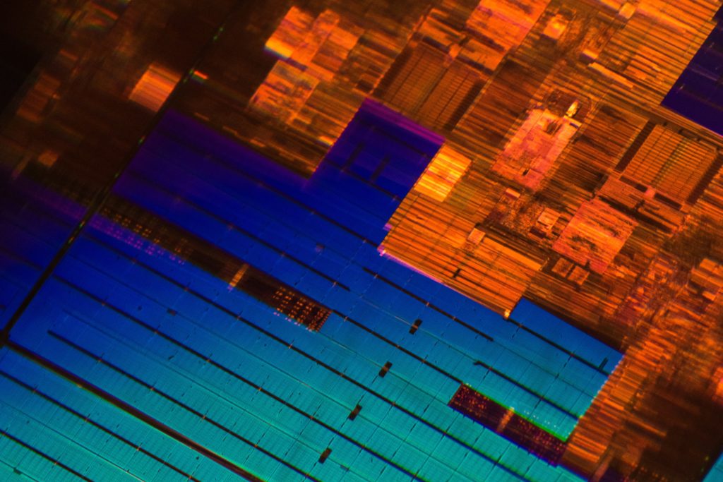
Photo by Mika Baumeister on Unsplash
THE GROWING NEED FOR HETEROGENEITY IN SEMICONDUCTOR
The computing world today is all about processing data in real-time. Developers expect their code to compile in milliseconds. Consumers expect applications to respond with zero-delay. All of this requires a seamless communication of different computing components is a must, mainly the software (code) and the hardware (chip) is required.
The computing world pitched against the human brain. The ultimate goal is to outperform the human brain’s ability to sense, think, and act. While computers are outpacing humans, the desire for the silicon brain is still ongoing. To eventually mimic the human brain’s capabilities (mainly – sense, think, and act) demands much more computational speed and optimization than available today.
To reduce the time to run the compiled code on the chip has pushed both the software and the hardware (semiconductor) industry.
The software industry has been consistently coming up with unique ways to handle the data to avoid thrashing. Efficient use of parallel programming to split the single process/task into threads has been one major factor. Software developers (mainly frameworks and programming ones) have also been pro-actively utilizing all the hardware features (SVMS – Scalar, Vector, Matrix, Spatial) to enable a rich user experience by processing the data faster.
To Reduce Time To Completion While Balancing Performance-Per-Watt Is Pushing The Need For Heterogeneous System Architecture
On another side, the hardware (semiconductor) industry is also innovating consistently (and trying to keep up with the software industry’s demand) to provide more performance-per-watt (PPW) that ensures the complex applications/workloads run efficiently. CPU/GPU/FPGA/ASIC design has seen not only architecture level innovations but also transistor-level. Shrinking transistor size made it possible to fabricate System-On-A-Chip (SoC) with billions/trillions of transistors in it. Transistor-level innovation has also allowed AI workloads to thrive. However, the SoC is hitting the design-wall and demands an innovative approach to cater to future workloads.
The SoC hitting the design-wall has pushed the semiconductor industry towards the Heterogeneous System Architecture (a.k.a. heterogeneous integration), which combines the best of the hardware capabilities to form a unique computing system. It allows the workloads to reduce time to completion while balancing the power-to-performance ratio.
Heterogeneous System Architecture requires unique semiconductor techniques that enable processing unit designs built using the best innovation out of the CPU, GPU, FPGA, and ASIC designs. It also drives the manufacturing process towards advanced technology nodes, packaging technology, and novel equipment.

THE SEMICONDUCTOR INNOVATION TO ENABLE HETEROGENEITY
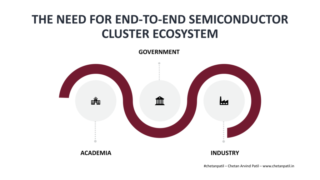
Academia and the industry has been putting forward ways to design and manufacture architectures that can fit the demand for heterogeneous system architecture.
The heterogeneous system architecture can be classified into three categories:
Synchronous: Synchronous heterogeneous system architecture uses a single voltage, frequency, clock, and power domain for all of its processing units/cores. Multiple clusters with cores can exist, with each cluster designed using a unique data pipeline technique such that clusters are capable of operating at different speeds/frequencies. However, the processing units/cores within a cluster, always run under the same voltage to the power scheme. Apart from the CPU, the GPU (running on separate voltage to power domain) is the only other type of processing unit that is part of the synchronous heterogeneous architecture system. ARM big.LITTLE is one such example.
Asynchronous: Asynchronous heterogeneous system architecture borrows everything from the synchronous one, but it may also allow processing units/cores level voltage, frequency, clock, and power scaling. The helps in fusing cores/units on the same SoC that improves PPW. Qualcomm’s Snapdragon is one such example. However, the data pipeline of all the cores in the Snapdragon is the same. In reality, an asynchronous heterogeneous system architecture is not yet available as it demands innovative transistor-level techniques to drive per core level power domain apart from different core designs. There are thermal challenges too. Asynchronous heterogeneous system architecture often has another type of processing units/cores (FPGA, ASIC, GPU) apart from the CPU.
Fusion: In many architectures that form heterogeneous system architecture, per-core/unit level power management is not available. Instead, a fusion heterogeneous system architecture technique of combining different types (CPU, GPU, FPGA, ASIC, NPU, XPU, and so on) of processing units/cores are used. Each of these processing units may have separate power management. AMD’s Accelerated Processing Unit is an example of fusion without per processing unit/core power management. Fusion-based heterogeneous system architecture demand advanced technology nodes, packaging technology, and novel equipment
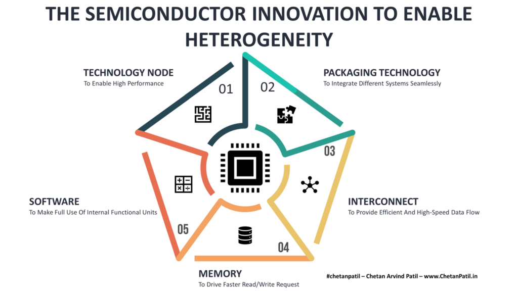
Whether one is designing synchronous or asynchronous or fusion heterogeneous system architecture, below are the five pillars of heterogeneous system architecture:
Technology Node: Integrating different processing cores/units to create a heterogeneous system architecture requires advanced technology nodes. The dies or the cores/units that get fused often have to get fabricated with the smallest possible transistor size. A true heterogeneous system architecture is supposed to make use of different technology nodes for the same integrated system. Example: A CPU inside a heterogeneous system architecture maybe 5nm, and the GPU might note be 5nm, and this pushes fabrication semiconductor companies to keep innovating on the transistor size and also on the device/transistor design/type (Planner FET, FinFET, GAAFET, MBCFET, etc.) Investing in Process Design Kit (PDK) and Electronic Design Automation (EDA) tools that can aid defect-free design is also required apart from developing fabrication facilities that can turn designs into silicon chips. All this puts pressure on the fabrication part of the semiconductor manufacturing process.
Packaging Technology: Heterogeneous architecture systems also require new ways to package dies/cores/units in a single platform. Multi-Die Multi-Chip Module based on chiplets based System-In-A-Package (SiP) is becoming a de-facto packaging standard for heterogeneous integration. Intel also has come up with many new solutions around heterogeneous integration. DARPA also has been pushing for Common Heterogeneous Integration and IP Reuse Strategies (CHIP) by collaborating with academia and the industry. To keep up with heterogeneous integration demand, the package technology roadmap has to be continuously revisited and aligned with the fabrication process.
Interconnect: Faster data movement is key to enabling optimization on heterogeneous system architecture. Whether it is within the processing core/unit or in-between two or more, high-speed bandwidth is vital. Many are proposing silicon photonics-based interconnection that provides a high-speed interface. There are still open questions about the power requirements for silicon photonics-based solutions. It might be possible to make use of a photonics-based solution with electrical interconnects. Researchers have also proposed several solutions for heterogeneous silicon photonic interconnects. Eventually, continuous research and development is a must, as tomorrow’s heterogeneous system architecture will be highly complex than today’s.
Memory: Like the high-speed interconnect, high-bandwidth memory is also vital for heterogeneous integration to enable faster read/write for processing core-to-core (unit-to-unit). It may also act as a memory side cache. Intel’s MCDRAM is one such example. AMD also has hUMA that provides Heterogeneous Uniform Memory Access (hUMA) for fusion-based heterogeneous system architecture. Recently, Micron launched 176-Layer NAND, which delivers high performance and density. Similar techniques are required to enable faster input/output in heterogeneous system architecture.
Software: Efficiently scheduling tasks on a heterogeneous platform needs APIs, as it allows developers to map software on the target heterogeneous system architecture efficiently that allows access to internal functional units and drivers. Intel’s oneAPI provides exactly such an interface for its heterogeneous platform. Another approach is utilizing the Heterogeneous System Architecture Intermediate Language (HSAIL) which acts as an ISA for parallel compute routines. Software developers need to also make use of all the internal hardware features to drive the fastest time to completion.
Irrespective of the type of heterogeneous system architecture used – synchronous, asynchronous, or fusion – the above five components are crucial to take full advantage of the heterogeneous system architecture and its capabilities.
THE IMPACT OF HETEROGENEOUS SYSTEM ARCHITECTURE AND INTEGRATION
The impact of deploying heterogeneous system architecture is largely on the semiconductor manufacturing process due to the highly complex nature of fabrication, testing, and assembling the different types of sub-units using heterogeneous integration technology.
FAB: Semiconductor FABs have to always keep innovating new types of transistor devices, interconnects (TSV Interposers, etc.), and most importantly the advanced technology nodes. The demand and pressure to produce zero-defect products while the transistor size decreases is a challenge in itself. FABs like TSMC and Samsung have already started work on 3nm well before large scale production of 5nm, which is a challenging task. Lower technology nodes will enable highly complex silicon that is most likely be part of the heterogeneous system architecture. Fabricating 7/5/3 nm and beyond not only requires massive investment (upward of $10+ Billion) but demands continuous research and development too in close collaboration with academia. Heterogeneous integration is a vital market and is pushing the FABs to get into the packaging domain. TSMC already has a TSMC-SoIC solution for heterogeneous chiplets integration. Soon Samsung and others follow the suit.
OSAT: OSATs are preparing by upgrading their packaging solution to align with the heterogeneous system architecture need. Fan-Out and SiP alike advanced packaging techniques require near-perfect materials and assembly recipes. ASE Global already has a roadmap to cater to the heterogeneous market. Other top OSATs like (Amkor, JCET, and SPIL) are also working on heterogeneous integration strategies. Amkor recently delivered the industry’s first package Assembly Design Kit to speed up accurate design and verification of heterogeneous integration package. Likewise, JCET and SPIL have also ramped up efforts for heterogeneous integration. Intel already has many in-house solutions for heterogeneous integration. Intel recently also won the State-of-the-Art Heterogeneous Integration Prototype (SHIP) project from the U.S. Department of Defence.
Heterogeneous System Architecture Is Pushing Semiconductor Manufacturing To Innovate
EQUIPMENT: The equipment required to not only enable accurate testing but also assembling (Chiplets, Multi-Chip Multi-Die Modules, and SiP) without compromising on the specification puts pressure on the suppliers. The majority of the OSATs providing heterogeneous solutions will have to either upgrade their infrastructure or invest in new facilities. It is directly pushing semiconductor equipment providers to come up with new solutions.
COST: Eventually, aligning FAB to OSAT to equipment for heterogeneous integration requires CapEx. The added cost to design, fabricate, test, and assemble will increase the cost of development. It might directly affect the cost of goods sold, and semiconductor companies will have to come up with new techniques for viable product development to breakeven.
YIELD: All of the above factors eventually impacts the yield. The more complex the product is, the difficult it is to keep the yield high. Maintaining a high yield becomes a challenge due to the new way to test the system. This challenge is due to the complex fabrication and assembly process brings due to the integrated approach. It also means investing in new test hardware, probe cards, and automated test machines to handle heterogeneous testing.
The heterogeneous system architecture is pushing the manufacturing and the design semiconductor industry to new possibilities. It will be crucial to see how both the FAB and OSAT innovate and work in close collaboration with EDA and FAB-LESS/IDM houses to drive the era of heterogeneous integration.