Image Generated Using 4o
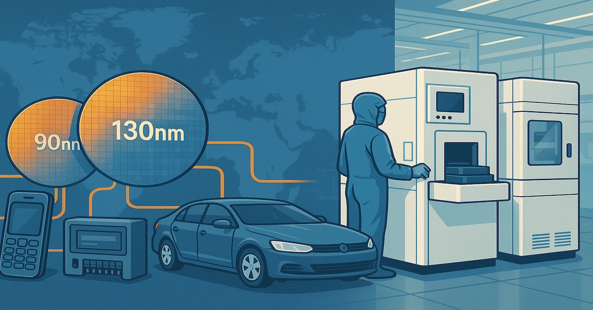
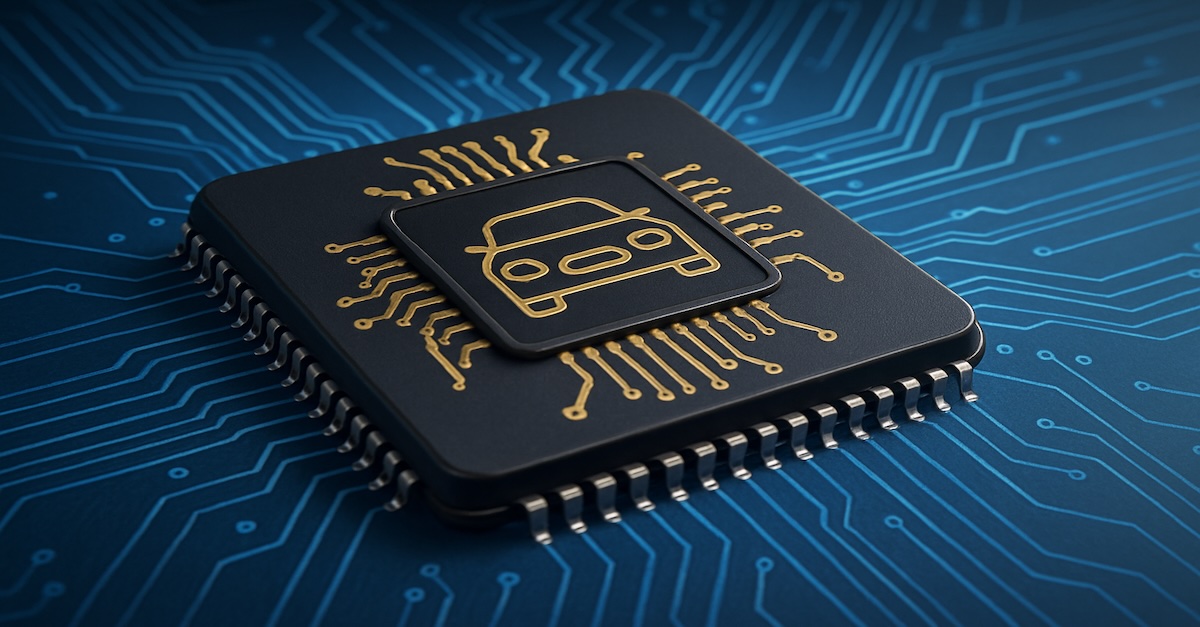
Automotive Semiconductor
Over the last two decades, the global automotive industry has undergone a fundamental transformation. A new class of automakers, established in the context of accelerating electrification, autonomy, and software-defined mobility, has emerged to challenge long-standing paradigms in vehicle design, manufacturing, and systems integration.
Unlike their legacy counterparts rooted in internal combustion and mechanical engineering, these companies were founded when semiconductors had become central to the vehicle’s core functionality.
From powertrain electrification and real-time sensor fusion to functional safety systems and edge computing for autonomous decision-making, modern cars have evolved into highly integrated, compute-intensive platforms.
This shift places semiconductors at the center of vehicle architecture, governing performance, user experience, system reliability, and over-the-air serviceability. In this new automotive landscape, chip architectures, embedded software, and electronic subsystems are now as critical to competitive differentiation as the engine or chassis once were.
Why Focus On New-Age Automakers?
Traditional carmakers are adapting to EVs and autonomy, but newer players are born-native to software, electric powertrains, and platform thinking. Many of these companies began with the core assumption that:
- Cars will be electric (or will use alternate fuel)
- Driving will be assisted or autonomous
- User experience will be digitally driven
- Supply chains will increasingly revolve around silicon
Their clean-sheet approach often puts them ahead on integration, over-the-air (OTA) updates, and leveraging high-performance chips. All while increasing the user experience.
New-Age Automakers Since 2005
In the past two decades, numerous new automotive manufacturers have emerged worldwide. Below is a comprehensive summary of these “new-age” automakers founded in 2005, covering passenger cars, commercial vehicles, and niche manufacturers. Each entry lists the company’s name, founding year, country of origin, market size (latest production volumes or valuation), target market segment, and vehicle type (EV, hybrid, etc.).
North America (United States And Canada)
The North American automotive sector has seen a wave of new companies born into the era of electrification, autonomy, and software-defined vehicles. These firms are redefining vehicle architecture and accelerating semiconductor integration across segments from luxury EVs to commercial platforms.
| Name | Founded | Country | Market Size (Latest Production / Valuation) | Target Market | Vehicle Type |
|---|---|---|---|---|---|
| Lucid Motors | 2007 (as Atieva) | USA | ~8,428 vehicles produced in 2023; ~6,000 delivered in 2023, market cap ≈ $7.7 B. | Luxury sedans (Lucid Air); upcoming SUV (Gravity). | EV (Battery Electric) |
| Rivian | 2009 | USA | 57,000 EVs produced / 50,000+ delivered in 2023; market cap ~$12 B. | Pickup trucks (R1T), SUVs (R1S), and delivery vans. | EV (Battery Electric) |
| Fisker Inc. | 2016 | USA | ~65,000 reservations; production began in 2023. Magna plant capacity ~120k/yr. | Premium SUVs (Ocean), compact EV (PEAR). | EV (Battery Electric) |
| Nikola Motor | 2014 | USA | 209 electric trucks delivered by end of 2023; market cap <$1 B. | Heavy-duty trucks (Tre semi tractor). | Hydrogen Fuel-Cell & Battery EV |
| Canoo | 2017 | USA | No mass production yet; Walmart ~4,500 vans ordered. Market cap ~$0.3 B. | Delivery vans, lifestyle vans, pickup trucks. | EV (Battery Electric) |
| Faraday Future | 2014 | USA | FF 91 deliveries began in 2023. Valuation declined from $3.4 B via SPAC. | Ultra-luxury SUVs (FF 91); future FF 81, FF 71. | EV (Battery Electric) |
| Bollinger Motors | 2014 | USA | Pre-production stage; acquired by Mullen Automotive in 2022. | Off-road trucks and commercial truck chassis. | EV (Battery Electric) |
| Aptera Motors | 2006 (revived 2019) | USA | Thousands of reservations for solar EV; no products delivered yet. | Solar-powered three-wheeler commuter vehicle. | EV (Battery Electric + Solar) |
| Workhorse Group | 2007 (as AMP) | USA | Delivered electric vans by 2020; low-scale operations ongoing. | Delivery vans and utility drones. | EV (Battery Electric) |
| Lion Electric | 2008 | Canada | ~550+ electric buses/trucks as of 2022; listed with ~$1.4 B valuation (2021). | Electric school buses and medium-duty trucks. | EV (Battery Electric) |
| Karma Automotive | 2014 | USA | Estimated revenue of $213.3M as of 2025. | Ultra-luxury sedans, coupes, and touring vehicles. | EREV & EV (Battery Electric) |
Sources: Information was compiled from a range of credible industry and news outlets, including Electrek, Lucid Motors Investor Relations, Companies Market Cap, Wikipedia, Electric Drives, Rivian Stories, Futurride, Reuters, Magna, CleanTechnica, Bloomberg, PR Newswire, Enterprise League, Driving Vision News, Faraday Future’s Medium blog, Techpoint Africa, TechCrunch, and Medium.
Europe
Europe has emerged as a hub for next-generation automotive startups, with companies targeting electric hypercars, solar mobility, and urban transport. These firms are advancing new powertrain architectures, modular manufacturing, and software-driven design across diverse market segments.
| Name | Founded | Country | Market Size (Latest Production / Valuation) | Target Market | Vehicle Type |
| Rimac Automobili | 2009 | Croatia | ~150 Nevera hypercars; valuation ~$2B post Porsche investment (2022). | Hypercars; EV powertrains for OEMs. | EV (Battery Electric) |
| Arrival | 2015 | UK | IPO valuation ~$13B (2021), dropped to <$10M (2023); assets sold to Canoo. | Urban vans and buses via modular microfactories. | EV (Battery Electric) |
| Polestar | 2017 | Sweden / China | ~51,500 EVs delivered in 2022; ~$6–10 B market cap (SPAC 2022). | Premium sedans, SUVs. | EV (Battery Electric, PHEV) |
| Automobili Pininfarina | 2018 | Italy | ~150 Battista hypercars planned; backed by Mahindra & Mahindra. | Luxury electric hypercars. | EV (Battery Electric) |
| Lightyear | 2016 | Netherlands | Built Lightyear 0 prototype; insolvency in 2023; rebooting Lightyear 2. | Solar-assisted long-range sedans. | EV (Battery Electric + Solar) |
| Sono Motors | 2016 | Germany | Developed Sion solar EV; project canceled in 2023, pivoted to retrofits. | Compact solar family cars (discontinued). | EV (Battery Electric) |
| Volta Trucks | 2019 | UK / Sweden | Pre-production of 16-ton electric trucks; funding and production hurdles. | Medium-duty logistics trucks. | EV (Battery Electric) |
| Microlino (Micro) | 2015 | Switzerland | ~150+ units delivered (2022–23); small-scale production in Italy. | City microcars (2-seater bubble cars). | EV (Battery Electric) |
Sources: Data compiled from Just Auto, Volvo Cars, Electronomous, TechCrunch, TechXplore, and MarkLines.
Asia – China
China has rapidly become a global epicenter for electric vehicle innovation, driven by a wave of startups founded in the last decade. These companies prioritize smart features, autonomous driving capabilities, and localized supply chains. Several have already reached significant production scale and are expanding globally, positioning China as a leader in next generation mobility.
| Name | Founded | Country | Market Size (Production / Valuation) | Target Market | Vehicle Type |
|---|---|---|---|---|---|
| NIO Inc. | 2014 | China | 160,000 EVs delivered in 2023; ~450k total by end of 2023. | Premium SUVs and sedans; focus on tech and battery swapping. | EV (Battery Electric) |
| Xpeng Motors | 2014 | China | 120,757 EVs in 2022; ~66k in 2023 (dip); rebound expected in 2024. | Smart sedans and SUVs; focus on in-house ADAS (XPILOT). | EV (Battery Electric) |
| Li Auto | 2015 | China | 376,000 vehicles delivered in 2023; fastest-growing Chinese EV startup. | Extended-range electric SUVs (EREV); family focused. | EREV (Extended-Range EV) |
| Weltmeister (WM) | 2015 | China | ~100k total units by 2022; entered bankruptcy in 2023. | Affordable crossovers and sedans for mass market. | EV (Battery Electric) |
| Leapmotor | 2015 | China | ~111,000 EVs in 2022; entering European markets in 2023. | Budget EVs including city cars, coupes, and mid-size sedans. | EV (Battery Electric) |
| Hozon Auto (Nezha) | 2014 | China | ~152,000 units in 2022; continued growth in ASEAN region. | Entry-level and mid-range EVs with good value proposition. | EV (Battery Electric) |
| Human Horizons | 2017 | China | Thousands of HiPhi X units sold since 2020; priced ~$100k+. | Tech-heavy luxury EVs; competing with premium global brands. | EV (Battery Electric) |
| Byton (defunct) | 2016 | China | Raised ~$1.2B; never launched. Ceased operations in 2021. | Smart luxury SUVs and sedans; failed to commercialize. | EV (Battery Electric) |
| BYD Auto | 2003 | China | Over 3 million vehicles sold in 2023; market cap > $80B. | Full spectrum: passenger cars, luxury, buses, commercial. | EV (Battery Electric), PHEV |
| MG Motor (SAIC) | 2007 (SAIC acquisition) | China | Over 800,000 vehicles sold in 2023 globally. | Affordable EVs and hybrids for global markets. | EV (Battery Electric), Hybrid |
| Aion (GAC Group) | 2017 | China | 480,000+ vehicles sold in 2023. | Mid-range and premium EVs (Aion Y, Aion LX, Hyper GT). | EV (Battery Electric) |
| Zeekr (Geely Group) | 2021 | China | Over 160,000 vehicles sold in 2023. | Premium performance EVs (Zeekr 001, Zeekr X, 009 MPV). | EV (Battery Electric) |
| Avatr (Changan + CATL + Huawei) | 2021 | China | Early stage; deliveries ramping in 2023. | High-end smart EVs with Huawei tech integration. | EV (Battery Electric) |
| IM Motors (SAIC + Alibaba) | 2020 | China | Low volume; deliveries began in 2022. | Tech-driven luxury EVs (IM L7, LS7). | EV (Battery Electric) |
| Rising Auto (SAIC) | 2021 | China | Rebranded from SAIC’s Roewe line; early growth phase. | Smart electric sedans and crossovers. | EV (Battery Electric) |
| Seres (AITO, Huawei JV) | 2016 | China | Partnered with Huawei; launched M5 and M7 models. | Hybrid and EV SUVs integrated with Huawei ecosystem. | EV (Battery Electric), EREV |
Sources: Data from CNEVPost, CarNewsChina, Technode, Reuters, TechCrunch, XPeng, and company investor portals.
Asia – Other Regions (India, Southeast Asia, Middle East, Africa)
Across India, Southeast Asia, the Middle East, and Africa, new automotive companies have emerged, addressing local market needs with electric mobility, affordability, and regional manufacturing. These companies range from high-volume e-scooter producers and electric bus makers to ultra-luxury and government-backed initiatives. Together, they represent a critical extension of the global shift toward sustainable and localized automotive innovation.
| Name | Founded | Country | Market Size (Production / Valuation) | Target Market | Vehicle Type |
|---|---|---|---|---|---|
| VinFast | 2017 | Vietnam | ~35,000 vehicles sold in 2023; market cap dropped from $85B to ~$6B. | Mass-market EVs (VF8, VF9); global expansion plans. | EV (Battery Electric) |
| Togg | 2018 | Turkey | 28,000 orders in first sales day (2023); scaling to 100k/year by 2025. | Electric SUVs and upcoming sedan/hatchback models. | EV (Battery Electric) |
| Ola Electric | 2017 | India | ~150,000 e-scooters sold (2022–23); electric car in pipeline. | Two-wheelers and future budget EV hatch for India. | EV (Battery Electric) |
| Pravaig Dynamics | 2011 | India | Prototype sedan launched; SUV under development for 2024. | Luxury EVs for Indian market; premium focus. | EV (Battery Electric) |
| Mobius Motors | 2010 | Kenya | Dozens of Mobius II SUVs built since 2015; halted in 2023. | Low-cost rugged SUVs for African roads. | Gasoline (ICE) |
| Kiira Motors | 2014 | Uganda | Building electric buses; scaling to 1,000+ units/year. | City buses and hybrids for East Africa. | EV & Hybrid |
| Innoson Vehicle Mfg | 2007 | Nigeria | Assembles a few thousand vehicles yearly; Nigerian govt support. | Low-cost cars, buses, pickups for West Africa. | Gasoline (ICE) |
| Ceer | 2022 | Saudi Arabia | First EVs expected in 2025; JV with Foxconn; BMW platform licensed. | EV sedans and SUVs for GCC and Middle East. | EV (Battery Electric) |
| W Motors | 2012 | UAE/Lebanon | Limited-run hypercars; expanding into electric/autonomous prototypes. | Ultra-luxury sports cars; now exploring EV-based law enforcement vehicles. | Gasoline (ICE), EV planned |
Sources: Data from Just Auto, Reuters, Techxplore, Medium, MarkLines, Dailysabah, Tribune PK, Wikipedia, and official company releases.
What This New-Age Automakers Mean For The Automotive Semiconductor Industry
This new generation of automakers is not merely a business disruption. A structural shift intensifies the demand for semiconductors across the automotive stack. A modern vehicle today, integrates more than 100 different types of silicon solutions, and this number is set to grow as autonomy, connectivity, and software-defined features expand.
What matters is not just chip volume but compute density and architectural dependency. ADAS, infotainment, and battery systems now rely on advanced SoCs and specialized silicon with performance levels approaching data centers.
Key implications for the semiconductor industry:
- Co-development is becoming standard as automakers involve chipmakers early in the design process
- Domain-specific architectures are evolving faster by leveraging innovations from AI, mobile, and high-performance computing
- Power electronics, safety systems, and battery management require integrated, real-time, capable solutions
- Regional supply chains and custom silicon initiatives are gaining momentum in strategic market
As new automakers scale, semiconductor companies must align closely with their timelines, architectures, and localized production strategies. Success will depend on delivering optimized computing and resilient system design.
Thus, semiconductors are no longer peripheral to vehicles. They are now the foundation of performance, safety, and product differentiation.