Image Generated Using DALL-E
What Is Semiconductor Product Development?
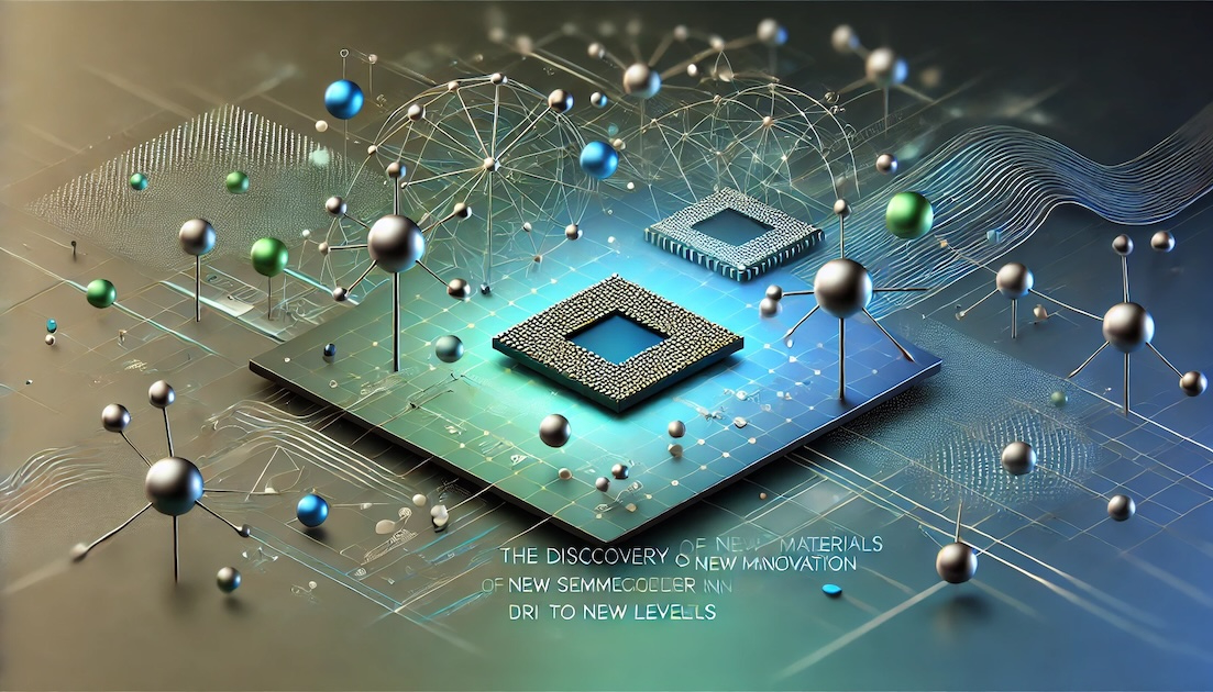
Semiconductor product development is the intricate process of transforming innovative semiconductor designs into fully functional, market-ready products. It bridges the gap between conceptual ideas and real-world applications by integrating critical disciplines such as design, testing, validation, manufacturing, and packaging.
This multifaceted process requires precision, meticulous planning, and seamless coordination across diverse teams, including silicon design, manufacturing, and beyond. Each stage is vital, as even minor errors can result in significant delays, increased costs, or product failures.
More than just technical execution, semiconductor product development drives technological progress. It is the foundation for advancements in consumer electronics, artificial intelligence, autonomous vehicles, and renewable energy.
Why Develop Skills For Semiconductor Product Development?
The importance of semiconductor product development skills cannot be overstated, as they are essential for driving innovation, meeting market and customer needs, ensuring reliability, achieving cost efficiency, maintaining future relevance, and aligning with market projections.
Product development skills empower professionals to anticipate and fulfill customer requirements, ensuring alignment with market needs and application-specific challenges. In aerospace, healthcare, and automotive industries, where reliability is paramount, these skills help ensure semiconductor products meet stringent quality and performance standards, fostering customer trust.
Additionally, efficient product development reduces time-to-market and production costs, enabling companies to stay competitive by optimizing yield and minimizing resource wastage. The dynamic nature of the semiconductor industry necessitates continuous skill development to remain relevant and address emerging trends such as AI-driven optimization, quantum computing, and sustainable manufacturing practices.
With the industry projected to grow significantly in the coming years, a strong skill set allows professionals to contribute effectively to product strategies, meeting current and future market needs.
Talent Demand
The demand for skilled professionals in semiconductor product development has reached unprecedented levels, fueled by the growing reliance on semiconductors across industries and the rapid pace of technological innovation.
Despite the industry’s growth, a significant skill gap persists. Many companies face challenges in finding industry-ready professionals capable of managing the intricate processes involved in semiconductor product development, from design to manufacturing.
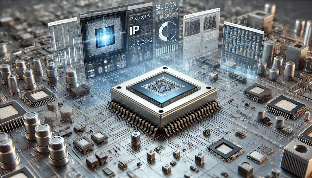
The complexity of modern semiconductor products requires expertise across several key areas, including:
- Product Design and Validation: Ensuring chips meet functional and performance requirements
- Yield Improvement and Reliability Engineering: Enhancing production efficiency and product dependability
- Advanced Packaging Techniques: Innovations like chiplet integration and 3D stacking which push the boundaries of performance and miniaturization
Talent demand is also surging in semiconductor hubs such as the U.S., Taiwan, South Korea, and India. These regions are home to leading global companies and a rising wave of startups, creating abundant career opportunities and making them epicenters for semiconductor innovation. This confluence of market growth, specialized demand, and regional activity underscores the urgent need for skilled professionals to shape the future of semiconductor technology.
Product Development And Market Correlation
As these advancements unfold, the demand for professionals with expertise in testing, quality assurance, and yield improvement will rise. Companies will increasingly seek individuals with technical and interdisciplinary skills to navigate this evolving landscape. The rewards are immense for those who invest in developing these competencies, ranging from lucrative career and growth opportunities.
In conclusion, semiconductor product development skills are the foundation of semiconductor product innovation. They ensure reliability, cost efficiency, and the creation of groundbreaking products. As the industry grows and evolves further, mastering these skills is not just an advantage but a necessity for thriving in this competitive and dynamic field.