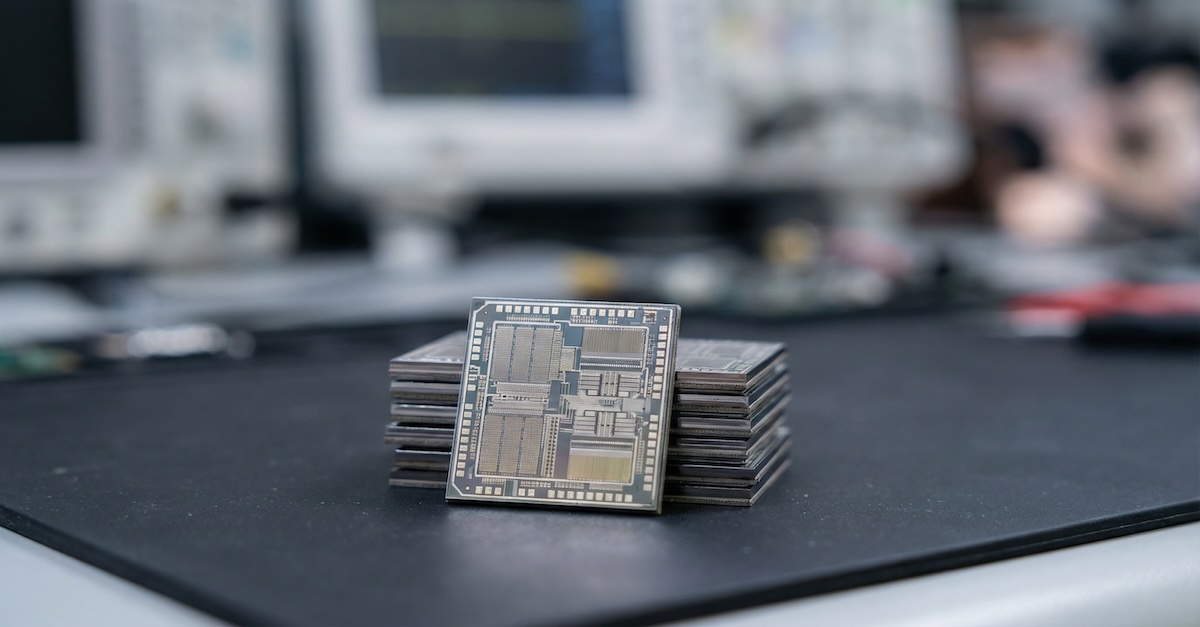
AI SoC development is now a board-level strategic choice, not just a technical decision. The question is no longer if AI acceleration is needed, but who should own the silicon. As AI workloads grow and diversify, companies must decide whether to build custom silicon in-house or outsource it. This decision affects performance, organization, capital, and long-term competitive standing.
On top, this crossroads marks a more profound shift in how value is created in semiconductors. AI models, data pipelines, software stacks, and silicon architectures are tightly coupled. When this coupling is strong, silicon becomes strategic. Where workloads are fluid or experimental, flexibility matters more than ownership. Companies must understand where they fall on this spectrum before choosing a path.
To make the right choice, companies must first gain clarity on their own priorities, capabilities, and competitive context. Only then can they decide whether to pursue custom silicon or leverage vendor solutions for AI.
In-House Control
Developing AI SoCs in-house offers a level of architectural and system control that is difficult to replicate through outsourcing. Companies can tailor compute, memory hierarchy, interconnects, and power management directly to their dominant workloads.
Over time, this alignment compounds into meaningful advantages in performance per watt, latency predictability, and system efficiency, especially for large, recurring AI workloads.
In-house development also establishes a direct feedback loop between silicon performance and deployment data. Real-world data informs ongoing design refinement and model optimization, which is critical as AI usage continually evolves.
This level of control, however, comes at a high cost. In-house AI SoC initiatives require long-term investment, cross-disciplinary talent, and internal management of risks such as yield, packaging, software, and supply chains. For organizations lacking scale or extended product timelines, these demands may outweigh the advantages.
Outsourcing Tradeoffs
Outsourcing AI SoC development, whether through merchant silicon or semi-custom partnerships, prioritizes speed, flexibility, and risk reduction. It allows companies to deploy AI capabilities rapidly. Organizations can adapt to evolving model architectures. They can also leverage mature software ecosystems without bearing the full cost of silicon ownership. For many organizations, this is not a compromise but a rational optimization.
Merchant platforms also benefit from aggregated learning across multiple customers. Yield improvements, reliability insights, and software tooling mature faster when spread across a broad user base. This shared progress can be hard for a single in-house program to match and is particularly true in the early stages of AI adoption.
Dimension
In-House AI SoC
Outsourced AI SoC
Architecture control
Full, workload-specific
Limited to vendor roadmap
Time to deployment
Multi-year cycles
Rapid, months-scale
Upfront investment
Very high
Lower, predictable
Long-term cost curve
Optimizable at scale
Vendor-dependent
Software–hardware co-design
Deep, iterative
Constrained, abstracted
Supply-chain exposure
Direct ownership
Shared with vendor
Differentiation potential
High
Moderate to low
That said, outsourcing inevitably limits differentiation at the silicon layer. Roadmap, dependency, supply constraints, and pricing dynamics are externalized risks. As AI becomes central to product identity or cost structure, these dependencies can become strategic bottlenecks. Convenience can turn into constraint.
Hybrid Direction
In practice, the industry is converging towards hybrid strategies rather than absolute positions. Many companies train AI models on merchant platforms but deploy custom silicon for inference. Others start with outsourced solutions to validate workloads. They internalize silicon once scale and stability justify the investment. This phased approach reduces risk and preserves future optionality.
What matters most is intentionality. In-house development should be driven by clear workload economics and platform strategy, not prestige. Outsourcing should be a strategic choice, not a default from organizational inertia.
The hybrid path works best when companies know which layers of the stack truly differentiate them. They should also know which layers are better left to ecosystem partners.
At this strategic crossroads, AI SoC decisions are about ownership of learning, not just ownership of transistors. Companies that align silicon strategy with data, software, and long-term business intent will navigate this transition successfully.
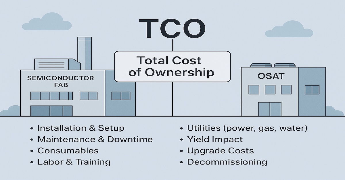
In the semiconductor industry, the cost of a tool, IP block, or software license is rarely limited to what appears on the purchase order. That figure is only the beginning of the financial story.
Total Cost of Ownership, or TCO, is a structured approach that enables companies to assess the full economic impact of acquiring, operating, and maintaining a product or service across its entire working life.
It encompasses the following:
Initial Purchase Cost: The upfront investment required to acquire the asset. This is often the most visible, yet frequently the smallest portion of the overall cost
Operational Costs: This includes recurring expenditures such as power, cleanroom real estate, workforce, license renewals, and consumables. These are day-to-day costs that quietly accumulate
Maintenance And Support: Over time, service contracts, spare parts, calibration routines, software patches, and staff training become essential to sustained performance
Downtime And Productivity Losses: Every hour of tool unavailability or design team obstruction, often caused by bugs, delays, or compatibility issues, translates directly into lost revenue and time-to-market pressure
End-of-Life Costs: When a system is retired, further investment may be required for decommissioning, migrating to newer technologies, or adapting legacy workflows
As the semiconductor business is continuously operated at the intersection of capital intensity and precision, a decision that reduces cost by a few percentage points can easily result in millions in hidden losses if it compromises reliability, throughput, or product quality.
Consider this:
A lower-cost tester that lacks precise thermal control may undermine test integrity, leading to field reliability issues and customer dissatisfaction
A less expensive IP block may have limited support or outdated documentation, resulting in costly silicon re-spin and substantial schedule delays
TCO encourages a shift in thinking from a short-term view focused on cost minimization to a longer-term view centered on operational value
In the end, TCO is not just a financial metric. It is a discipline that helps teams make more efficient.
TCO In Different Parts Of The Semiconductor Business
Every segment of the semiconductor value chain, whether in fabrication, testing, design, or packaging, carries its own distinct Total Cost of Ownership profile. Each function introduces a unique set of variables that influence long-term cost. Understanding how TCO manifests across these areas is not just a matter of accounting accuracy.
Let us break it down by function:
Segment
Initial Cost
Operational Cost
Support & Maintenance
Downtime/Hidden Cost
FAB Equipment
Capital investment in tools like lithography, etch, deposition
Utilities, cleanroom usage, consumables like gas and chemicals
Production disruptions, scalability limits during expansion
It is essential to avoid costly surprises, manage operational risk, and make informed, future-focused investment decisions. Over time, this perspective often separates companies that scale efficiently from those that struggle to contain hidden losses.
Hypothetical Examples And Mistakes To Avoid
Let us consider few hypothetical examples to explain TCO.
Example 1: To reduce capital expenses, a semiconductor firm selected a low-cost test handler for high-volume automotive lines. However, the handler underperformed thermally in production, leading to a 4 to 6 percent yield drop and multiple customer quality issues. The recovery costs far outweighed the initial savings, highlighting that long-term reliability matters more than price.
Example 2: Another company reused an older IP block to avoid new licensing fees. The IP was incompatible with the current process node and poorly documented. Integration issues went undetected, resulting in a post-silicon bug and a costly response. The delay stretched timelines and added over three million dollars in rework.
Decision
Goal
Unseen Cost
Low-cost test handler
Save CapEx
Yield loss, quality issues
IP reuse
Avoid licensing fee
Silicon respin, delays
Budget EDA tool
Reduce license cost
Engineering inefficiency
Used fab tool
Save equipment cost
Increased downtime
Example 3: A design team switched to a cheaper simulation tool to cut license costs. However, the tool was unstable, with slow runtimes and limited support. Engineers lost valuable time managing tool issues, leading to delays and lowered team efficiency. The short-term savings came at the cost of long-term productivity.
Example 4: A fabrication facility bought a used etch tool to reduce capital investment. While initially functional, it lacked software updates and required frequent maintenance. Uptime suffered, disrupting wafer cycle times and impacting line stability. The operational drag soon eclipsed the upfront benefit.
These cases show that decisions to save money upfront can introduce hidden costs in quality, time, and yield. TCO helps teams evaluate the full financial impact beyond the purchase price.
Integrate TCO Thinking Into Engineering And Business Decisions
TCO is more than a finance metric. It is a way of planning that must be built into engineering, procurement, and operational decisions. For engineers, this means looking beyond technical specs and considering long-term impacts such as debug effort, uptime, integration complexity, and reusability. Asking what might go wrong after deployment often reveals the fundamental cost drivers.
Procurement teams should work closely with engineering to move beyond basic quotes. They must evaluate uptime history, support terms, maintenance cycles, and parts availability. Eventually, two tools with similar specs can vary widely in lifetime cost due to serviceability and consumable usage.
Who
Action For TCO Thinking
Engineers
Consider long-term debug, yield, and integration risks
Procurement
Evaluate beyond price: uptime, service, and lifecycle support
Business leaders
Use 3–5 year TCO models in planning and ROI analysis
Cross-functional teams
Share lessons learned and maintain internal TCO benchmarks
Business leaders can use three to five-year TCO models to improve cost forecasting and ROI decisions. For example, a lower-cost tester may reduce CapEx but limit throughput, while a higher-end tool may improve unit economics in volume production. Planning with this view leads to more resilient product execution.
Finally, TCO thinking must be shared across functions. Engineering, finance, quality, and operations should jointly define benchmarks and track performance over time. Reviewing past decisions helps organizations avoid repeating costly oversights.
Yield in semiconductor manufacturing is a complex concept that measures the efficiency and effectiveness of the production process. It is usually expressed as the ratio of the number of good dies (functional chips) to the total number of dies made on a wafer.
As the industry moves towards smaller nodes and more complex architectures, yield becomes increasingly essential. It affects the economic viability of a fabrication facility and plays a pivotal role in determining its competitive advantage in a market that values efficiency and innovation.
Let us explore the technical aspects of yield in semiconductor manufacturing and its crucial role in ensuring the competitiveness of new fabrication facilities.
Why Yield Is Vital For New FABs
Yield is vital for new semiconductor fabrication plants (FABs) because it fundamentally determines their economic success and competitive position in the market. High yield – the proportion of functional devices produced from the total manufactured – directly reduces the cost per functional die, enabling new FABs to offer competitive pricing while maintaining profitability.
This cost efficiency is crucial given the substantial capital investment required to establish a new FAB. Moreover, achieving high yield early in operations accelerates capital recovery and signals process maturity and reliability to potential customers and partners. It also enhances time-to-market for new technologies, providing a competitive edge in an industry where rapid innovation is critical. High yield also ensures product quality and reliability, strengthening the FAB’s reputation and fostering customer trust.
In essence, yield impacts every aspect of a new FAB’s success, from financial viability and market competitiveness to technological leadership and brand reputation. Further, below is a table summarizing why yield is vital for new FABs:
Aspect
Importance
Explanation
Economic Viability
Cost Efficiency
High yield reduces the cost per functional die, which is crucial for profitability in an industry with tight margins. Lower costs per die improve the overall economic efficiency of the FAB.
Capital Recovery
Maximizing yield accelerates the return on the substantial capital investments required for new FABs by increasing the output of sellable products, thus improving cash flow and financial health.
Competitive Advantage
Time-to-Market
High initial yields enable new FABs to bring products to market faster, providing a competitive edge in rapidly evolving technology sectors where delays can result in lost market opportunities.
Customer Acquisition
Demonstrating high yield reflects process maturity and reliability, making the FAB more attractive to potential customers and partners who are seeking dependable manufacturing services.
Market Positioning
Superior yield can differentiate a FAB in competitive bids, as clients prefer manufacturers capable of delivering high-quality products consistently, enhancing the FAB’s position in the market.
Technological Leadership
Process Innovation
Achieving high yield signifies successful implementation of advanced manufacturing techniques and technologies, establishing the FAB as a leader in process innovation and capability.
Scaling Advanced Nodes
Maintaining high yield at smaller process nodes (e.g., 7nm, 5nm) is challenging; success in this area demonstrates technical prowess and leadership in cutting-edge semiconductor fabrication.
Quality Assurance
Product Reliability
High yields generally indicate fewer defects, leading to more reliable and durable products, which is essential for customer satisfaction and long-term success.
Brand Reputation
Consistently high product quality enhances the FAB’s reputation, fostering trust and loyalty among clients and end-users, and can lead to increased business through positive references and word-of-mouth recommendations.
A new FAB must invest in cutting-edge technology like advanced lithography and metrology tools to ensure precision and minimize defects. Real-time process control systems, such as Advanced Process Control (APC) and Statistical Process Control (SPC), help monitor and adjust manufacturing parameters to maintain optimal conditions.
Cleanroom management and stringent contamination protocols are equally essential, as even minor particulate contamination can significantly reduce yield. Furthermore, strong partnerships with suppliers ensure high-quality materials and components, while Design for Manufacturability (DFM) practices help optimize chip designs for production efficiency. However, it’s important to remember that a well-trained workforce is not just a part of the process but a critical element in managing complex tools, troubleshooting yield-impacting issues, and contributing to continuous improvement efforts.
Yield optimization relies heavily on data analytics and AI, which can detect subtle correlations in process data, predict failures, and suggest real-time process adjustments. By focusing on these areas and fostering a culture of continuous improvement and employee engagement, new FABs not only enhance their yield performance and recover capital investments faster but also have the potential to establish a reputation for reliability and quality in the semiconductor market.
Ultimately, achieving high yield is a multifaceted challenge that requires commitment at all levels, from leadership down to operators on the production floor. With the right strategies in place, new FABs can not only achieve their yield goals but also secure a competitive edge in the fast-paced semiconductor industry, inspiring a sense of ambition and drive in the audience.
The ultimate goal of any yield improvement initiative is to drive higher ROI by balancing upfront investments with long-term financial benefits. Yield effectiveness is not just about technical excellence but about aligning process optimization, equipment investments, and workforce expertise to produce maximum value. For new FABs, high-yield effectiveness accelerates capital recovery, improves profitability, and positions the FAB as a cost leader in a highly competitive industry, bringing significant financial benefits and a promising future.
As a direct indicator of operational efficiency, product quality, and market readiness, yield is the most critical lever a new FAB has for ensuring sustained financial success and achieving the highest possible ROI. It is not just a technical metric but the key to unlocking the economic power of the FAB and reassuring stakeholders about the FAB’s performance.
Achieving high-yield effectiveness in a new FAB is fundamentally about optimizing Return on Investment (ROI). Yield directly influences an FAB’s ability to produce more functional chips per wafer, reducing the cost per die while maximizing output from a given set of resources. In semiconductor manufacturing, where even a 1% improvement in yield can lead to millions of dollars in cost savings, the relationship between yield and ROI becomes crystal clear.
The capital-intensive nature of new FABs, with billions of dollars spent on cutting-edge equipment, infrastructure, and personnel, demands that every dollar invested in improving yield leads to measurable financial returns. High yield ensures that the FAB operates most efficiently, turning a significant proportion of raw materials into marketable products and minimizing waste, downtime, and rework.
A semiconductor FAB is a production plant where devices such as integrated circuits are manufactured. These facilities are equipped with clean rooms and sophisticated equipment to precisely control environmental conditions, ensuring the high quality and purity required for semiconductor manufacturing.
Outsourced Semiconductor Assembly and Test (OSAT) companies take over post-fabrication. They cut the manufactured wafers into individual chips, package them, and conduct rigorous testing (in many cases before cut/dicing) to ensure they meet the required specifications. OSATs allow semiconductor companies to focus on the highly specialized chip design process (and fabrication) without bearing the brunt of assembly and testing processes.
The Need To Invest In Semiconductor FAB And OSAT
Investing in semiconductor FABs and OSAT facilities is a strategic move for many countries and corporations aiming to bolster their technological infrastructure, economic resilience, and strategic autonomy.
As global demand for electronics continues to surge, the need for more integrated circuits rises, thus enhancing the strategic importance of having in-house semiconductor manufacturing and assembly capabilities.
Investing in semiconductor FABs and OSAT facilities is not just a financial decision but a strategic one that can significantly influence a nation’s or corporation’s technological and economic landscape.
The positives of such an investment revolve around enhancing economic activity through job creation and infrastructure development, boosting technological innovation, securing supply chains, and ensuring strategic independence. These benefits are crucial in positioning a country at the forefront of the global technological race.
Aspect
Description
Economic Growth
Establishing FABs and OSATs involves significant capital expenditure, leading to job creation and infrastructure development, stimulating local economies.
Technological Leadership
Local FABs and OSATs foster innovation in semiconductor technologies, propelling advancements and maintaining a competitive edge in global markets.
Supply Chain Security
Having domestic FABs and OSATs reduces reliance on international suppliers, securing critical technology supply chains against global disruptions.
Strategic Independence
Domestic manufacturing of semiconductors ensures a steady supply of crucial components, vital for national security and technological sovereignty.
Establishing FABs and OSATs can catalyze sustained economic growth and technological leadership. By fostering a self-sufficient and innovative environment, a country can significantly reduce its dependencies, enhance global competitiveness, and ensure a more secure future.
Moreover, the local development of semiconductor technologies can drive advancements in various high-tech sectors, cementing a country’s position as a technological leader.
The Negatives Of Semiconductor FABs And OSATs
Despite their significant advantages, establishing and operating semiconductor FABs and OSATs come with considerable challenges. The high costs of setup and maintenance, coupled with the environmental impact and the cyclic nature of the semiconductor market, pose potential risks.
Additionally, the geopolitical sensitivities associated with semiconductor supply can lead to vulnerabilities in international relations and trade.
Aspect
Description
High Initial Costs
The cost of setting up and maintaining semiconductor manufacturing facilities can be prohibitively high, with risks of obsolescence due to rapid technological advances.
Environmental Impact
Semiconductor production is resource-intensive and generates significant hazardous waste, posing challenges for sustainable operations.
Economic Volatility
The semiconductor market is notoriously cyclical, which can lead to financial instability for regions heavily invested in these sectors.
Geopolitical Sensitivity
Being a critical component in numerous applications, semiconductor supply can be disrupted by international tensions and trade policies.
While the negatives present formidable challenges, they necessitate robust planning and mitigation strategies to manage effectively. The high initial investments should be weighed against long-term economic returns, and environmental impacts require sustainable practices and technologies to operate.
Furthermore, navigating the cyclical economic patterns and geopolitical landscapes demands adaptive strategies that ensure stability and profitability in the volatile semiconductor market. These considerations are essential for countries and corporations aiming to capitalize on the benefits while minimizing the risks associated with semiconductor manufacturing.
What The Future Holds
The decision to establish new semiconductor FABs and OSAT facilities involves weighing significant positives against formidable negatives. At the same time, they promise economic growth, technological advancement, and many other benefits. Conversely, environmental impact, financial volatility, and geopolitical entanglements should also be considered.
As the global landscape evolves, the strategic calculation for investing in such infrastructure will continue to change, reflecting the dynamic nature of the semiconductor industry. Each country or corporation must carefully assess its capabilities and needs to make informed decisions that align with its long-term strategic goals.
By embracing innovation, prioritizing sustainability, enhancing supply chain resilience, and adapting to geopolitical and market dynamics, the semiconductor industry can expect robust growth and continued relevance in the global economy.
In conclusion, the future of semiconductor FABs and OSATs is promising but requires adaptation to a rapidly changing technological landscape and global context.
The dominance of semiconductor giants like NVIDIA, with a market capitalization exceeding $3 trillion, and TSMC, valued at nearly $700 billion, among the top 10 largest companies globally, underscores the seismic shift towards a semiconductor-driven economy.
These (and many other) firms, pivotal in the semiconductor industry, highlight the sector’s critical role in underpinning most of today’s technological landscape. With semiconductors at the heart of an array of technologies – from artificial intelligence and data centers to consumer electronics and automotive systems – this industry’s influence mirrors the transformative power of oil in the previous century.
The stark representation of semiconductor firms among the elite global corporations (by market cap) illustrates their economic significance. It signals the dawn of an era where technological innovation, powered by semiconductors, is the new currency of global dominance.
This transition spotlights the undeniable fact that semiconductors have become the ‘new oil,’ essential for fueling the future of global technology and economy.
The rise of semiconductors can be traced back to the mid-20th century, marking a revolution in technology and engineering. Initially, the industry was focused on simple diodes and transistors. Still, by the 1960s, the invention of the integrated circuit paved the way for the microprocessors that would eventually power personal computers, mobile phones, and many other devices.
By the 1980s and 1990s, advancements in semiconductor technology allowed for exponential increases in computational power, adhering to Moore’s Law, which predicted a doubling of transistors on a chip approximately every two years. This growth has continued into the 21st century, with the semiconductor market size reaching over $425 billion in revenue by the early 2020s, underlining the critical role of semiconductors in global technological progress.
The semiconductor industry, projected to reach a $1 trillion market by 2030, plays a pivotal role in the global economy, contributing to approximately $3 trillion in GDP from 1995 to 2015 and an additional $11 trillion in indirect impact. This industry’s significance is further highlighted by its accelerating growth, doubling its importance relative to global GDP over the last three decades. Moreover, the U.S. semiconductor sector’s investment in R&D, totaling $58.8 billion in 2022, underscores its commitment to innovation, with R&D expenditure surpassing 15 percent of sales for over two decades.
The semiconductors’ trajectory has been remarkable, evolving from essential components to the backbone of advanced computing systems and consumer electronics. This surge reflects the expanding demand for electronic devices, cloud computing, and data centers, driven by digital transformation across industries. The semiconductor’s role in technology’s future is underscored by substantial investments in research and development, aiming to push the boundaries of what these tiny yet powerful chips can achieve.
In today’s rapidly evolving world, semiconductors are the cornerstone of modern technology, quietly powering the digital age from behind the scenes.
They are not just components; they are the architects of our digital reality, enabling the seamless operation of networks, processing vast amounts of data, and developing cutting-edge technology. As the world ventures into an era defined by artificial intelligence (AI), the significance of semiconductors becomes even more apparent, cementing their status as indispensable drivers of global progress and innovation.
Without these microscopic marvels, the technological advancements that define our current lifestyle and promise an even more interconnected and intelligent future would not be possible.
The semiconductor industry is not just a part of the future economy. It is poised to be a cornerstone, driving innovation and growth across multiple sectors. Here are several statistics-based arguments that illustrate this trend:
ASPECT
STATS
Market Growth
The global semiconductor market was valued at around USD 425 billion in 2020 and is expected to grow at a CAGR of approximately 6.8% from 2021 to 2028, driven by demand in automotive, consumer electronics, and industrial applications.
Innovation And RnD Investment
The industry allocates 15-20% of sales revenue to RnD, surpassing many other sectors, underscoring a commitment to innovation and future growth.
Impact On Other Industries
Semiconductors underpin modern technology and are vital for AI, 5G, and IoT advancements. For example, 5G deployment relies on advanced semiconductor technology.
Economic Multiplier Effect
Each job in the semiconductor sector generates approximately 4.89 additional jobs in other economic sectors, demonstrating the high value-add of semiconductor products and their extensive supply chain.
Global Supply Chain And Trade
The semiconductor industry is a worldwide trade powerhouse with international sales and supply chains, supporting economic growth and fostering international technological exchange.
Sustainability And Energy Efficiency
Semiconductors enable energy-efficient solutions like electric vehicles and smart grids, contributing to reduced energy consumption and alignment with global sustainability goals.
Semiconductor Everywhere
Governments worldwide are rapidly awakening to the critical importance of semiconductors, recognizing them as the backbone of modern technology and a crucial element of national security and economic prosperity. In an era where technology underpins every aspect of daily life, from communication and entertainment to transportation and defense, the role of semiconductors has become increasingly central.
This realization is prompting nations to reassess their strategic priorities, leading to a surge in investments, policy reforms, and international collaborations to secure semiconductor supply chains and boost domestic production capabilities.
By acknowledging the semiconductor industry’s pivotal role in advancing technological innovation, ensuring military readiness, and driving economic growth, governments are now placing semiconductor strategy at the forefront of national agendas, marking a significant shift towards securing technological sovereignty in a rapidly evolving global landscape.
Here are eight ways in which countries are investing in semiconductors:
ASPECT
DETAILS
Funding And Tax Incentives
Countries provide grants for new factories, R&D subsidies, and tax breaks to attract semiconductor companies, supporting manufacturing and research.
Building Semiconductor Ecosystems
Efforts are made to create comprehensive semiconductor ecosystems, including manufacturing, design, RnD, and support for startups, universities, and research institutions.
Strategic Partnerships And Alliances
Forming strategic partnerships and alliances with nations, companies, and research institutions to secure supplies and advance technological capabilities.
Education And Workforce Development
Investing in education and training programs to develop a skilled workforce, including specialized university programs and technical training.
Research And Development Investments
Making significant investments in RnD to advance semiconductor technology, focusing on next-generation materials, chip design, and manufacturing processes.
Supply Chain Resilience
Taking measures to ensure the resilience of semiconductor supply chains, including diversifying sources and investing in domestic manufacturing capabilities.
Attracting Foreign Investment
Working to attract foreign semiconductor companies through incentives, regulatory support, and infrastructure development, integrating more deeply into the global supply chain.
National Security Measures
Implementing measures to protect semiconductor industries for national security, including restrictions on foreign investments and securing intellectual property rights.
Take Away
In the contemporary landscape, where semiconductors play a pivotal role in driving technological advancement and economic growth, understanding the multifaceted impact of this industry is essential for a diverse array of stakeholders.
For students, the ascendance of semiconductors underscores the critical importance of engaging with STEM disciplines, highlighting the opportunity to be at the forefront of technological advancements. Professionals, particularly those within the realms of technology and manufacturing, are reminded of the necessity to perpetually enhance their skill sets in alignment with the industry’s dynamic nature. For the industry at large, the pivotal role of semiconductors emphasizes the imperative of fostering innovation, facilitating international collaborations, and prioritizing research and development to maintain competitiveness on the global stage. Governments are called upon to recognize the strategic importance of the semiconductor sector, advocating for policies that bolster industry support, ensure the resilience of supply chains, and promote technological progress. Collectively, these insights articulate the transformative influence of semiconductors and their indispensable position in steering the direction of our digital future.
The semiconductor industry’s influence extends far beyond the confines of technology firms, touching upon education, professional development, industrial strategy, and governmental policy. As the world delves into the implications of semiconductors’ ubiquitous presence in our digital era, examining the takeaways for critical groups such as students, professionals, the broader industry, and government entities is imperative.
This perspective highlights the critical importance of semiconductors and sheds light on the collective and individual roles in embracing and advancing this dynamic field of semiconductors.
Over the last few years, coopetition has increased around the semiconductor industry. It shows how semiconductor-dependent companies align their business to what works best for the market.
Some of the examples of coopetition are from the semiconductor industry:
TSMC, Bosch, Infineon, And NXP Jointly Invest In European Semiconductor Manufacturing Company (ESMC).
Bosch, Infineon, Nordic, NXP, And Qualcomm Jointly Invest In A Company Aimed At Advancing The Adoption Of RISC-V Globally By Enabling Next-Generation Hardware Development.
Mediatek Partners With NVIDIA To Provide Full-Scale Product Roadmap To The Automotive Industry.
NVIDIA, ASML, TSMC, And Synopsys Set Foundation For Next-Generation Chip Manufacturing.
Apple Announces Multibillion-Dollar Deal With Broadcom For Components Made In The USA.
Qualcomm Announces Multi-Year Collaboration With Sony To Deliver Next Generation Smartphones.
Qualcomm Collaborates With Hyundai Motor Group On Purpose-Built Vehicle Infotainment.
Intel, Ericsson Expand Collaboration To Advance Next-Gen Optimized 5G Infrastructure.
Synopsys And Samsung Foundry Deepen Collaboration To Accelerate Multi-Die System Design For Advanced Samsung Processes.
Synopsys And Arm Strengthen Collaboration For Faster Bring-Up Of Next-Generation Mobile SoC Designs On The Most Advanced Nodes.
Synopsys And Samsung Collaborate To Deliver Broad IP Portfolio Across All Advanced Samsung Foundry Processes.
Cadence Extends Collaboration With TSMC And Microsoft To Advance Giga-Scale Physical Verification In The Cloud.
Intel And ASML Strengthen Their Collaboration To Drive High-NA Into Manufacturing In 2025.
Imec And ASML Sign Memorandum Of Understanding (MoU) To Support Semiconductor Research And Sustainable Innovation In Europe.
AMD And Qualcomm Collaborate To Optimize Fast Connect Connectivity Solutions For AMD Ryzen Processors.
And, The List Goes On….
However, coopetition can also be challenging, requiring companies to balance their competitive and cooperative interests. It is essential for companies to carefully consider the risks and benefits of coopetition before entering into a coopetition arrangement.
Nevertheless, as the semiconductor industry evolves around the AI and More Than Moore strategy, one can expect to see even more coopetition arrangements.
The semiconductor manufacturing industry is highly complex, requiring a well-planned and managed resource allocation, product flow, and supply chain.
Effective management of the factories and other resources is also essential to ensure high-quality semiconductor goods. It includes carefully considering capacity, material planning, logistics, and other aspects of the production process.
Planning: Semiconductor Manufacturing Is Highly Complex, Requiring A Well-Planned And Managed Resource Allocation.
Manufacturing: Effective Management Of The Factories And Other Resources Is Also Essential.
With the right tools and strategies in place, companies can ensure that their semiconductor manufacturing operations smoothly are running while meeting customer demand.
More so when the capacity and complexity of the wafer production process constantly increase and will become more crucial in the chiplets and More-Than-Moore era.
Additionally, it is vital to have a reliable forecasting system for resource planning and allocation. Moreover, the material flow should adhere to industry standards. With such measures, semiconductor manufacturing can support the end customers far better.
Along the path to achieving the high-quality management of semiconductor manufacturing, issues like – downtime, cost, and process optimization to resource allocation, people management, logistics, capacity planning, and inventory management – all play an essential factor.
Quality: High-Quality Management Requires A Detailed Process.
Cost And Time: Cost And Time Are Factors That Can Impact The Production Process.
In addition to these operational issues, semiconductor manufacturers must also navigate the ever-changing market landscape and gain insight into customer needs to remain competitive.
Additionally, cost and time are factors that can impact the production process. Thus, navigating these various hurdles is a critical part of semiconductor manufacturing management as it will ensure optimal production of semiconductors.
Industries and companies worldwide are focused on creating value, without which it is not possible to survive the customer-driven market. The semiconductor industry is no different and has consistently added value over the last four decades.
The value created by the semiconductor industry has enabled different other connected industries. It is evident based on the fact that semiconductor-focused solutions have become critical pillars for businesses that need innovative semiconductor-powered products.
Value Flow: Solutions and products that take the semiconductor and other connected industries forward.
To generate value consistently requires executing flawless strategy, which the semiconductor industry (mainly companies focused on product development) has carried out for decades. This value generation ranges from technology node, equipment, process development, package technology, raw material improvement, etc. There have been examples where such plans have failed, but the number of successful value creation-focused is considerably high.
Segment: Creating segments that add value to the industry is the first step toward developing vital semiconductor value flow.
Planning: Planning focuses on ensuring the development of segments leads to high-value creation, which demands consistent innovation.
Creating value that drives the industry forward demands long terms focus and planning. It starts with focusing on segments that can add value. It can be new equipment, FABs to OSATs capacity building, new semiconductor devices, and several other sub semiconductor chain-focused segments. Along with a clear segment definition, robust planning is a must-have.
Creating segments and planning a long-term roadmap is a must-have for value flow. The other two parts of value flow creation are investment and learning.
The investment focuses on building the capital and human resource to drive the segments that will bring the needed value to the semiconductor industry. And learning focuses on course correction required to ensure the value flow of new or existing domains does not go off track.
Investment: Focuses on enabling required resources and teams that can constantly innovate the value flow.
Learning: Capturing errors and failures to make necessary course correction is vital to creating a robust value flow.
Value flow has become an integral part of the semiconductor industry. Mainly due to the growing dependency on semiconductor products. Such a dependency demands highly focused value flow management. If not done correctly, it can often lead to situations similar to semiconductor shortages.
The semiconductor industry is bound to grow in the coming decades. It is valid both from market size and numerous products that will get manufactured. Value flow needs to be more robust to achieve these goals, and the semiconductor industry thus will have to keep finding new avenues to make the new and existing value flow more resilient and innovative.
There are several parts to semiconductor product development, and without cross-industry collaboration and standardization, it is impossible to move forward (next-gen solutions).
Collaboration and standardization have triggered several innovative solutions that have only taken the semiconductor industry forward. These strategic approaches come in different forms. Some are between two or more semiconductor-focused companies, many driven by consortiums of several companies (semiconductor and non-semiconductor). Irrespective of the approach, the focus is to bring new semiconductor technologies.
Collaboration Benefits: It fosters the environment where one or more companies can share the knowledge to enable next-gen devices that can create future markets while expanding the current one. Examples of such collaboration are many. Collaboration between XPU developers and non-XPU developers is one. The reason one relies on the other and has to follow a collaborative approach to ensure the end products (desktops, laptops, smartphones, etc.) work flawlessly.
Standardization Benefits: One of the impacts of standardization is that it allows product development knowledge sharing irrespective of the resources and capital any given company has. An example of this can be all USB or Wi-Fi-driven silicon solutions as it follows a standard protocol and empowers companies to build on top of it. Recently announced Universal Chiplet Interconnected Express is also one such example.
The two positive impacts of collaboration and standardization are knowledge sharing and learning. Given how high-tech the semiconductor industry is, the knowledge transfer and learning approach enables a thriving business and expands the reach of semiconductor products.
Knowledge: Sharing technical knowledge that helps the industry move forward is only possible via active collaboration.
Learning:Capturing learnings based on old solutions allows the development of new solutions for the emerging market, which also requires standardization and continuous collaboration.
The semiconductor industry-wide standards from the past decades have already shown the world several innovative solutions. Majority of which came out of active collaboration. It is also true that no given semiconductor company can thrive without active cross-industry partnerships. More so when the devices today require multiple and different types of solutions.
In the end, the goal of collaboration and standardization in the semiconductor industry is to drive a new age of innovation, something the global semiconductor ecosystem has done very well for the last four to five decades.
Apart from the technical benefits, the two other vital impacts of collaboration and standardization are the expansion of business via existing or near markets along with the ability to launch next-gen devices. It is evident from the fact that today’s smart devices that were only possible due to the active collaboration of different types of semiconductor companies.
Several of these strategic collaborations are proprietary. Which is also required to ensure the different businesses can create a niche market for themselves. On another side, there have been several open collaborations. All of which have moved the industry forward and have allowed design and manufacturing companies to come up with solutions to power next-gen solutions.
Business: Different types of semiconductor businesses benefit from standardization as it creates a level playing field on the top of which companies can develop new solutions.
Next-Gen: Emerging solutions (chiplets and photonics as an example) are only possible via industry-wide standardization. Otherwise, the speed of adoption will be slow.
Active collaboration is also key to bringing new solutions forward. Semiconductor lithography solution is one such example. It has been able to leap forward only due to the long-term strategic planning and focus. Some of which have also been with academia.
As the need to push for More-Then-Moore solutions grows further, the importance of semiconductor collaboration and standardization will grow too and make the semiconductor ecosystem more advanced than ever before.
There is not a single industry that does not rely on strategic partnerships. The semiconductor industry is no different, and semiconductor companies have to rely on a strategic partnership to achieve the goal of a successful product launch.
The semiconductor industry has several different segments. While the two major segments are design and manufacturing, several other critical segments are needed to empower the design to manufacturing solutions. These solutions originate from companies located in different countries, and the solutions developed powers billions of tiny silicon devices.
It will not be wrong to say that the semiconductor industry is one of the most distributed. A single semiconductor chip with billions of transistors takes more than ten to twenty different companies to work together. In many cases, companies are global. In such scenarios, any disruption on one location or shortage (in the case of manufacturing) can impact the end-to-end supply chain.
Connected: Semiconductor industry is one of the most connected industries out in the market, and different companies have to work together to get the product launched.
Dependent:Semiconductor companies are dependent on each other, and this is also the primary reason why not a single region or country fully dominates in the semiconductor chain. It is always global collaboration that leads to innovative silicon chips.
While countries without a stronghold on semiconductor design and manufacturing are focused on building in-country capabilities, the reality is that it not only requires several years (or decades) but is also impossible to create an end-to-end in-country semiconductor ecosystem. There will always be areas (not one, two, but several) for which every country will have to rely on others. It is where the technology-focused long-term partnership is required, without which it is impossible to keep the semiconductor chain intact.
The semiconductor industry is a global one. Any given semiconductor company is strategically involved with different semiconductor and non-semiconductor companies. Imagine disrupting this global connected and dependent semiconductor ecosystem and how it will impact day-to-day product development activities.
Over the last four decades, different regions across the globe have made their mark on specific solutions required by semiconductor-focused companies. Some regions are good at design, some at semiconductor manufacturing, a few at semiconductor equipment, and many on raw materials (including bare wafers). Eventually, all of the regions are powering each other.
Global: Semiconductor product development always follows a global approach and the primary reason is the resource and solution dependency.
Decentral:Decentralization is a key part of the semiconductor industry. Different regions have to work together, without which product development will halt.
This connected, dependent, global and decentralized approach is the primary reason why the semiconductor industry is growing double-digit year on year. This approach is never going to change, and this is why different countries need to work together to enable next-gen solutions for ever demanding and ever growing semiconductor market.