Category: CHIPLET

  • The Hurdles In Adopting Chiplets As Semiconductor More-Than-Moore Solution

    The Hurdles In Adopting Chiplets As Semiconductor More-Than-Moore Solution

    Photo by Laura Ockel on Unsplash


    Chiplet is undoubtedly the most suitable semiconductor design and manufacturing solution to scale complex chips reaching the reticle limit. Several silicon products have already adopted chiplet, mainly processors. These products have showcased that using multiple chiplet can significantly improve performance. All while not worrying about the reticle or device constraints.

    Several initiatives have come up to speed up the adoption rate of chiplet. Like, Universal Chiplet Interconnect Express (UCIe), which is an open specification for bridging different types of chiplets from the same or multiple vendors by standardizing the interconnectivity, quality, reliability, and several other aspects that are critical to a chip build using the disaggregated approach. Similarly, a few more industry and academia consortiums have emerged, focusing on several criteria to ramp up mass chiplet adoption.

    Even with all these steps, certain fundamental hurdles remain, and careful planning is needed before any company uses chiplets to develop silicon chips.

    Wafer management is one such hurdle. As the number of chiplets per silicon design increases, so will the number of wafers, adding cost to the already costly process.

    Wafer Management:

    – A chip designed using chiplets methodology will consist of multiple wafers, with each wafer focused on producing a specific silicon chiplet

    – As an example, an XPU with N chiplets will require N number of wafers, and thus, as many wafer management flows

    – Merging these N wafers into a single package via heterogeneous integration is going to be complex, time-sensitive, and prone to errors

    – Apart from this, the fabricating, testing, and assembly process of each of these wafers will add extra cost that may be more than the aggregated approach

    With each wafer comes the challenge of achieving the reference yield.

    Yield:

    – Chiplets with less complex designs (due to the splitting of larger die areas into multiple chiplets) will still have to go through the required yield check process

    – The more the number of chiplets, the more time intensive the yield check becomes (multiple data sources)

    – The hurdle here is also to manage the specifications

    – So far, the best possible way to mitigate this would be to consolidate the larger block into a single chiplet and repeat the same with other blocks of a larger silicon chip

    – Even then, the questions of managing and achieving the yield remain, and multiple-chiplet only adds to the already complicated flow


    Picture By Chetan Arvind Patil

    Efficient testing of chiplet is another hurdle.

    Test:

    – Every chiplet will have a unique wafer, and if multiple such wafers are consolidated to create an end silicon chip, testing is crucial and, by default, part of the process flow

    – With multiple flows, the amount of effort needed to test increases.

    – It leads to more resources and testing hardware

    – Eventually, adding to the testing cost

    – If this is more than the cost of testing an aggregated chip, the industry must develop a process to optimize it

    To turn multiple chiplets into working silicon chips is also about managing overall development costs. Today, the cost of chiplet will be higher than the aggregated approach due to increased resources required by the multiple chiplets.

    Cost:

    – Fabricating, testing, and assembly cost is increasing with the increase in the test complexities

    – When working with chiplets, managing the expense to prevent higher costs of working with multiple wafers (each wafer = chiplet) is crucial. Otherwise, it will not seen as a valid alternative aggregated flow

    – Chiplet should be seen as a More-Than-Moore solution but also as a cost-optimization solution

    – Eventually, the goal is also to manage the increased cost of designing chips as large as a reticle (26 mm by 33 mm)

    – Lastly, the human resources required for chiplet will be more than needed for an aggregated approach. Which will add to the cost too

    No doubt, chiplets have the potential to address several aggregated technical and business challenges. However, the chiplets will be limited to certain types of silicon chips, like XPUs.

    For chiplets to be disruptive, mentioned manufacturing flow-driven challenges should be resolved. Otherwise, the journey towards and beyond sub-1nm will be more aggregated than disaggregated.
  • The Hurdles For Semiconductor Chiplets

    Photo by Maxence Pira on Unsplash


    The semiconductor industry continually faces challenges as it shrinks transistor sizes to increase performance. One promising solution to achieve this goal is the use of chiplets. Chiplet is small; independent silicon dies that can be interconnected to create a larger, more powerful chip – chiplets.

    Chiplets can provide several advantages over traditional monolithic chips, are customizable to meet the specific needs of a particular application, and can also be fabricated using different types of silicon nodes, which can reduce costs and improve performance.

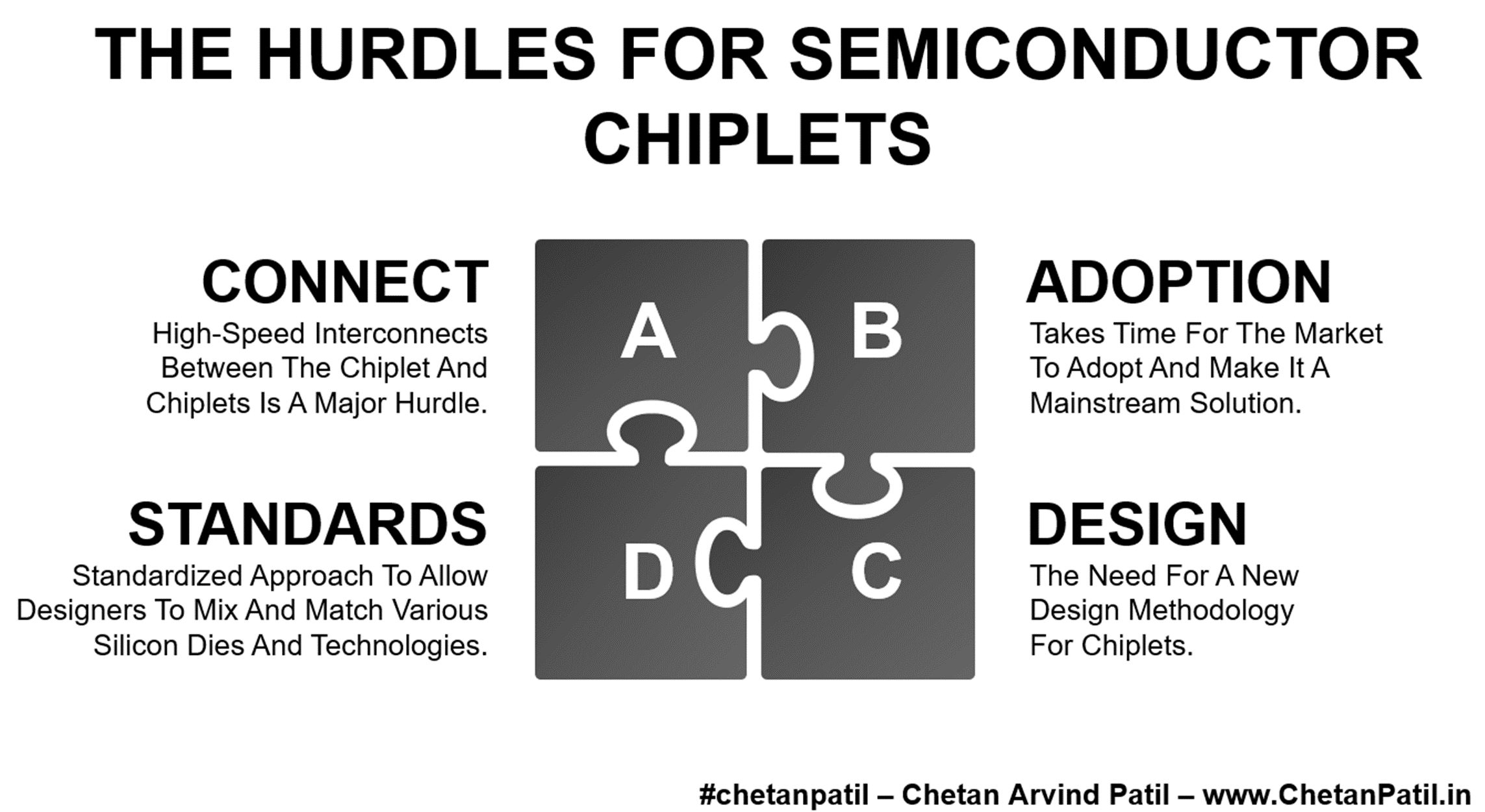
    Connect: High-Speed Interconnects Between The Chiplet And Chiplets Is A Major Hurdle.

    Adoption: Takes Time For The Market To Adopt And Make It A Mainstream Solution.

    However, there are also some critical hurdles that chiplets will need to overcome before they can become mainstream. One challenge is the need for high-speed interconnects between the chiplet and chiplets. These interconnect must handle the high data rates required by modern applications while being reliable and secure.

    Another challenge is the need for a new design methodology for chiplets. Traditional chip design methods must be better suited for chiplets. New techniques must adhere to the requirements of several semiconductor companies trying to adopt chiplets to develop a disaggregated approach.


    Picture By Chetan Arvind Patil

    Market adoption is also a hurdle for chiplets as new design and manufacturing technology. It will take time for the market to adopt and make it a mainstream solution.

    Despite these challenges, chiplets have the potential to revolutionize the semiconductor industry. They offer several advantages over traditional monolithic chips and could help address the industry’s challenges.

    Design: The Need For A New Design Methodology For Chiplets.

    Standards: Standardized Approach To Allow Designers To Mix And Match Various Silicon Dies And Technologies.

    Chiplets can go a long way in addressing existing challenges, such as the rising cost of producing monolithic chips, and thus open the door to new, innovative chip designs. Eventually, by allowing designers to mix and match various silicon dies and technologies, chiplets can be used to create custom chips tailored to specific applications.

    The future of chiplets is uncertain, but they have the potential to be a significant disruptive force in the semiconductor industry. Only time will tell if they can overcome their challenges and achieve widespread adoption.


  • The Semiconductor Road Towards Chiplets

    The Semiconductor Road Towards Chiplets

    Photo by Luan Gjokaj on Unsplash


    Semiconductor products are struggling to meet the demand to balance power, performance, and area requirements. The challenge to enable efficiency is increasing while there is also a need to meet new technological requirements without adding bottlenecks. Such challenges are slowly becoming impossible tasks whereby the innovation is hitting a technical wall and is now pushing semiconductor design and manufacturing towards a new era.

    To overcome these hurdles semiconductor industry is looking to increase the adoption rate of chiplets. Chiplet is also becoming a stepping stone toward the new era of silicon devices (mainly XPUs) that provide better power-performance management. Such a solution also allows more features while not worrying (for now) about bottlenecks.

    The fundamental reason for adopting semiconductor solutions like chiplets is to ensure that the process technology can be efficiently used by disaggregating the solution across multiple blocks, thus ensuring the critical blocks get the most advanced solutions.

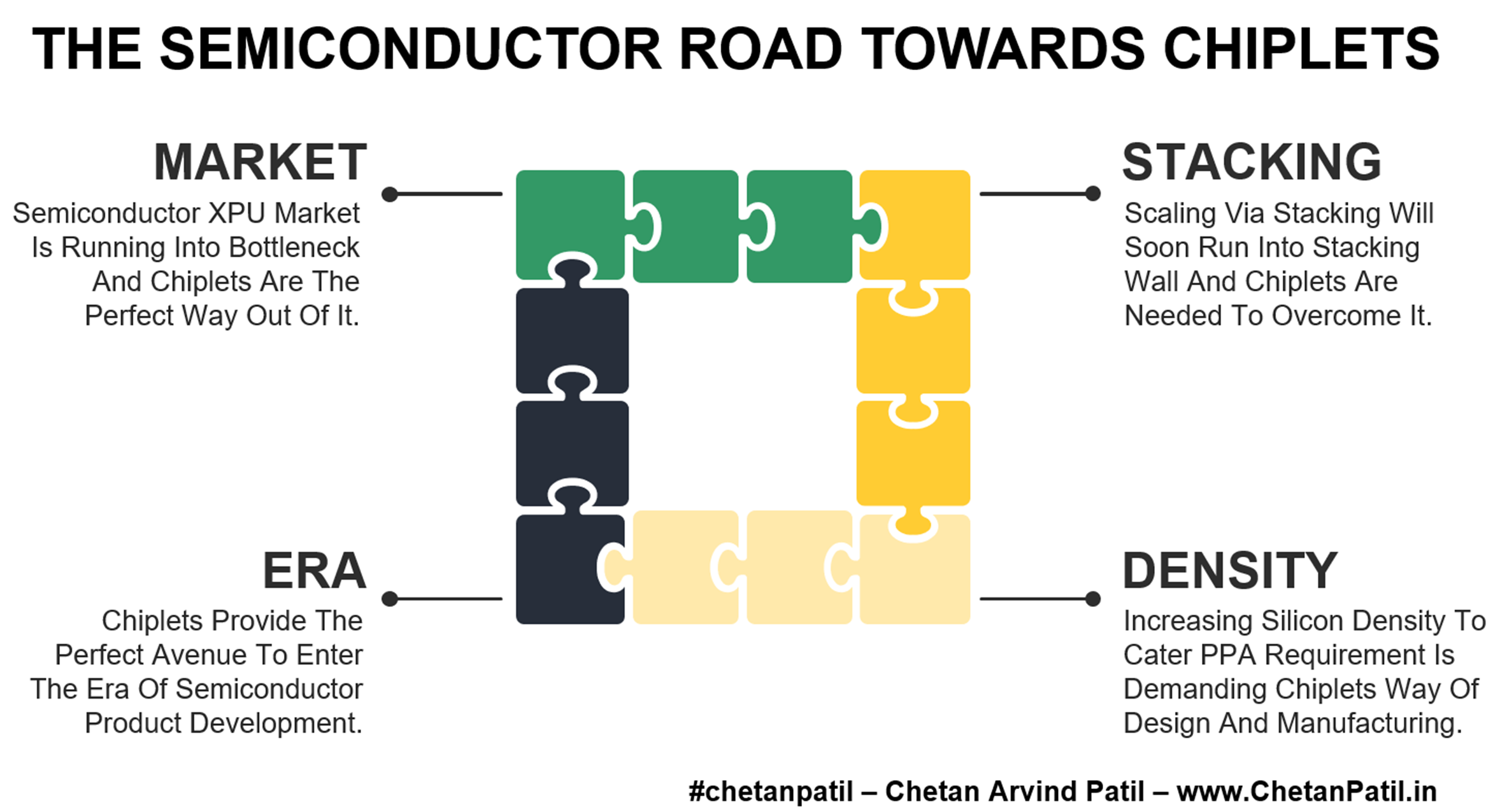
    Market: Semiconductor XPU Market Is Running Into Bottleneck And Chiplets Are The Perfect Way Out Of It.

    Stacking: Scaling Via Stacking Will Soon Run Into Stacking Wall And Chiplets Are Needed To Overcome It.

    However, the adoption of chiplets at a large scale requires a semiconductor road. The inception of the semiconductor road for chiplets is the market, which has been demanding near-bottleneck free features to cater to the world that is processing data.

    Adopting a chiplet solution is to overcome stacking-related thermal and mechanical issues. It has become a concern for XPU-type devices where the need to double the transistors is increasing faster than ever. It has also created new scaling-related hurdles. To solve the scaling bottleneck, chiplets provide a better avenue by allowing the more horizontal area to enable designers and manufacturers to bring new features.


    Picture By Chetan Arvind Patil

    The market requirement is for smaller but powerful silicon devices. It is a must-have for solutions that form the base of on-the-go computing systems like XPUs. However, slowly the ability the integrate more features without impacting the silicon area has become a bottleneck, mainly for the XPU designers. Such a bottleneck directly creates density issues which can potentially lower the performance metric of new solutions.

    Chiplets are by default the better-known solutions to the density-related problem as it allows scaling to be done with the help of packages. However, for chiplets, it is important to consider the cost and time to manufacture. Otherwise, the positive technical impact of chiplets can easily get void by the negative business impact.

    Density: Increasing Silicon Density To Cater PPA Requirement Is Demanding Chiplets Way Of Design And Manufacturing.

    Era: Chiplets Provide The Perfect Avenue To Enter The Era Of Semiconductor Product Development.

    The semiconductor industry is always looking for a solution that can enable a new type of semiconductor product. The ultimate goal of such solutions is to move the computing industry towards a new era. Chiplets do provide an avenue to do so and the semiconductor road taken by the industry has already started enabling a new type of chiplets-driven solutions that are also creating a new level of competition which is eventually going to benefit the industry at large.

    The semiconductor market focused on XPUs is already demanding more chiplets-driven architecture, which in turn is enabling the solution to mitigate near-future scaling and density solutions, and this technical semiconductor road has certainly started the new era for the semiconductor industry and will also enable new types of devices.


  • The Long-Term Impact Of Semiconductor Chiplets

    The Long-Term Impact Of Semiconductor Chiplets

    Photo by Louis Reed on Unsplash


    Chiplets are changing the way complex products like XPUs getting designed and manufactured. Its impact is how modular the new XPU solutions are becoming. This modularity is paving the way for new-age IP-driven XPU design and manufacturing and opening up features that were not easy to deploy due to the need for the aggregated approach.

    As with any new semiconductor process and technology, the vital factor is the long-term impact of such new solutions. In the case of chiplets, it has already started to impact design and manufacturing methods.

    The positive long-term impact of chiplets is providing the ability for XPU developers to enable solutions in the angstrom era by leveraging the disaggregated approach. It is also opening up a new design approach that allows chip architects to leverage different types of IP blocks and also provides the ability to enhance block-level processing capability due to the disaggregated manufacturing.

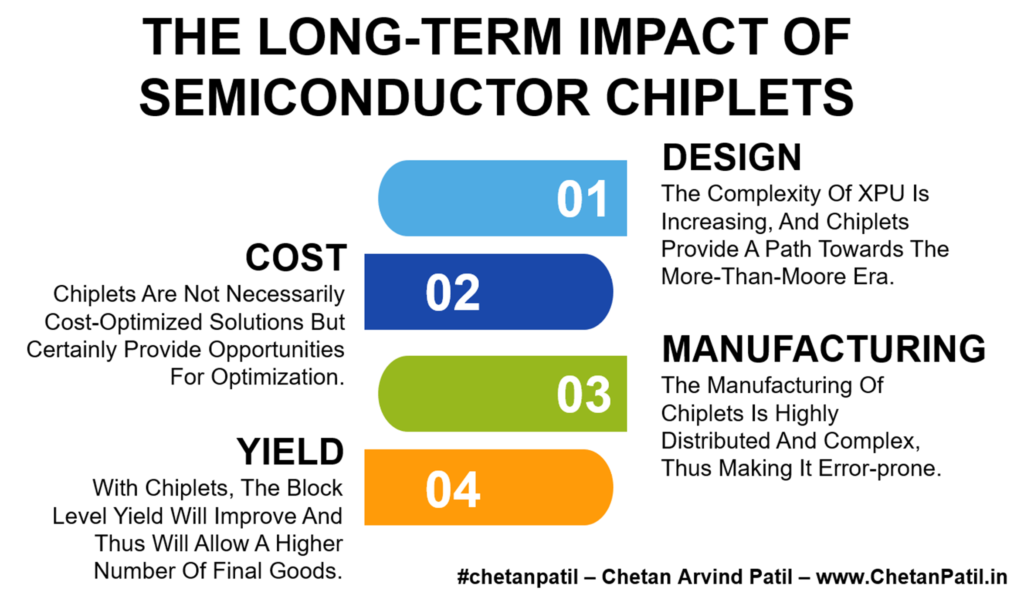
    Design: The complexity of XPU is increasing, and chiplets provide a path towards the More-Than-Moore era.

    Cost: Chiplets are not necessarily cost-optimized solutions but certainly provide opportunities for optimization.

    From the cost point of view, chiplets may be costly to manufacture due to the die level disaggregation that will require multiple silicon wafers and capacity. The manufacturing flow will also become more complex. Until the chiplet adoption speeds up, the early adopters will have to spend more capital.

    However, as the adoption increases, the manufacturing processes are bound to become optimized. It will then drive better cost-optimized manufacturing of chiplets-driven XPUs.


    Picture By Chetan Arvind Patil

    Distributed processing of chiplets at the manufacturing side brings new challenges. More so when the packaging of chiplets becomes a critical process. The complex manufacturing flow on the packaging side can drive a higher error rate if the process is not validated correctly before mass production.

    There are processes available to ensure the new manufacturing process (chiplets) leads to positive results. However, until the chiplets-inspired chips are mass-produced, there will always be a possibility of errors and such errors will impact yield and cost.

    Manufacturing: The manufacturing of chiplets is highly distributed and complex, thus making it error-prone.

    Yield: With chiplets, the block level yield will improve and thus will allow a higher number of final goods.

    The aggregated approach of XPU design and manufacturing does not often lead to higher yields. Disaggregated manufacturing of chiplets enables higher yield. Mainly due to the ability to take the complex critical blocks as separated die.

    Chiplets design and manufacturing methods are still in the early days. As adoption and usage grow, the positive and negative long-term impacts will be more visible. Meanwhile, today, chiplets are indeed the most promising More-Than-Moore era solutions.