For more than a decade, AI silicon has evolved along two independent trajectories. On one side sat throughput-optimized architectures built to train massive models across thousands of accelerators. These prioritize raw FLOPS, memory bandwidth, and scaling efficiency. On the other hand, latency-optimized designs were engineered to deliver fast, deterministic inference. They are used at the edge or in tightly constrained data center environments. Each solved a different bottleneck, served a different buyer, and spoke a different architectural language.
That division made sense when training and inference occurred separately. Training was infrequent and centralized in hyperscale data centers. Inference ran continuously, near users, under strict latency and power limits. Chip companies specialized: some in large-scale matrix math, others in microsecond responsiveness, real-time scheduling, and efficient small-batch execution.
The AI boom of the last few years has collapsed that neat divide. Large language models, multimodal systems, and agentic AI now blur the boundary between training and inference. Models are fine-tuned continuously and updated frequently. They are increasingly deployed in interactive settings. Here, response time directly shapes user experience. In this environment, solving only for throughput or only for latency is no longer sufficient.
As a result, a structural shift is underway in the semiconductor industry. Chip companies that historically dominated one side of the equation are responding. They are acquiring, partnering, or redesigning their architectures to address the other side. When latency-first and throughput-first philosophies converge under a single entity, the impact extends far beyond product roadmaps. This shift reshapes how AI computing is designed, deployed, and monetized across the entire ecosystem.
Latency Versus Throughput And Economic Tradeoffs
Latency-optimized and throughput-optimized chips differ in almost every major design choice, reflecting different workload, integration, and cost assumptions.
Latency-focused architectures emphasize minimizing response time for individual requests by optimizing for small batch sizes, predictable execution paths, and efficient handling of workloads with extensive control logic. These chips commonly serve inference for recommendation systems, conversational AI, and autonomous systems.
In contrast, throughput-focused architectures maximize processing of large, regular workloads through aggressive parallelism, making them suited for the prolonged training of massive neural networks.
The table below summarizes key architectural distinctions:
Dimension
Latency-Optimized Architectures
Throughput-Optimized Architectures
Primary Goal
Minimize response time
Maximize total compute per unit time
Typical Workload
Inference, real-time AI
Training, large-scale batch jobs
Batch Size
Small to single-request
Large, highly parallel batches
Memory Behavior
Low latency access, caching
High bandwidth, streaming
Interconnect
Limited or localized
High-speed, scale-out fabrics
Power Profile
Efficiency at low utilization
Efficiency at high utilization
Software Stack
Tight HW-SW co-design
Framework-driven optimization
As a result, this convergence exposes inefficiencies when architectures stay siloed. Throughput-optimized chips can struggle to deliver consistent, low-latency inference unless you overprovision. Latency-optimized chips often lack the scaling efficiency needed for large-scale model training. The economic consequence is fragmented infrastructure and a rising total cost of ownership.
What Happens When One Company Owns Both Sides Of The Equation
When a single chip company unites the industry’s best latency and throughput solutions, the impact transcends simple product expansion. This move redefines design philosophy, software stacks, and customer value propositions.
From an architecture standpoint, convergence enables more balanced designs. Unified companies can deliberately trade off between peak throughput and tail latency, rather than blindly optimizing for a single metric. We are already seeing accelerators that support flexible batching, adaptive precision, and mixed workloads, allowing the same silicon platform to serve training, fine-tuning, and inference with fewer compromises.
Software is where the impact becomes most visible. Historically, separate hardware platforms required separate toolchains, compilers, and optimization strategies. Under one entity, these layers can be harmonized. A single software stack that understands both training and inference enables smoother model transitions from development to deployment, reducing friction for customers and shortening time-to-value.
The table below highlights how unified ownership changes system-level outcomes:
Aspect
Fragmented Latency / Throughput Vendors
Unified Architecture Vendor
Hardware Portfolio
Specialized, siloed products
Co-designed, complementary products
Software Stack
Multiple toolchains
Unified compiler and runtime
Customer Workflow
Disjoint training and inference
Seamless model lifecycle
Infrastructure Utilization
Overprovisioned, inefficient
Higher utilization, shared resources
Innovation Pace
Incremental within silos
Cross-domain optimization
Strategic Control
Dependent on partners
End-to-end platform leverage
Strategically, this convergence decisively strengthens negotiating power with both hyperscalers and enterprise customers. Vendors delivering a coherent training-to-inference platform command stronger positions in long-term contracts and ecosystem partnerships.
Consequently, there is also a competitive implication. Unified vendors can shape standards and influence frameworks. They can guide developer behavior in ways fragmented players cannot. As AI computing shifts from a commodity to a strategic asset, control over both latency and throughput becomes industrial power.
New Center Of Gravity In AI Compute
The convergence of latency and throughput architectures marks a turning point for the AI semiconductor industry. A technical distinction is now a strategic divide. Some companies offer isolated solutions. Others provide integrated platforms.
As training and inference workloads merge, chip companies treating AI compute as a continuous lifecycle will win. This approach avoids viewing each step as a separate phase. Combining latency and throughput optimized solutions brings architectural balance. It enables software coherence and economic efficiency.
This shift marks a new center of gravity for the AI ecosystem, as compute is no longer just about speed or scale. Now, it is about adaptability and utilization.
It also supports changing AI needs without frequent infrastructure redesign.
Computer architecture defines a computing system’s structure, component interaction, and trade-offs for performance, efficiency, cost, and reliability at scale. Architecture balances instruction sets, microarchitecture, memory hierarchies, and system-level design to meet workload requirements. Instruction encoding, pipeline depth, and cache topology shape both the physical silicon and the chip’s performance.
Unlike computer organization or circuit implementation, architecture focuses on what the system does and how it exposes those capabilities to software. This includes the instruction set interface and the abstract execution model visible to compilers, operating systems, and applications.
In semiconductor-powered computing, these architectural choices shape how transistors, the fundamental semiconductor devices, coordinate to deliver throughput, latency, efficiency, and workload specialization.
Modern computing systems no longer rely on a single silicon engine for all performance demands. Instead, heterogeneous architectures combine general-purpose cores with specialized accelerators. This enables systems to efficiently handle workloads including sequential control logic, parallel processing, machine learning, graphics rendering, and signal processing.
This architectural shift is a key lever for innovation as transistor scaling slows and thermal constraints tighten. By tailoring structures to specific workloads, semiconductor-powered computing continues to advance. This occurs even as raw process scaling alone becomes less effective.
Architectural Paradigms And Workload Mapping
As computing workloads diversified, no single architectural paradigm could efficiently meet all performance, power, and scalability demands. Computer architecture therefore evolved along multiple paths, each optimized for how computation is expressed, how data moves, and how parallelism is exploited. These paradigms are direct responses to workload characteristics such as instruction complexity, data locality, concurrency, and latency sensitivity.
Modern systems now integrate multiple architectural paradigms within a single platform. Control-heavy functions run on general-purpose cores, while compute-dense kernels are offloaded to parallel or specialized engines. This workload-driven mapping shapes not only performance, but also silicon area allocation, power delivery, memory hierarchy, and interconnect design.
Architectural Paradigm
Architectural Focus
Strengths
Best-Suited Workloads
General-Purpose CPU Architecture
Low-latency execution, complex control flow, instruction-level parallelism
Flexibility, strong single-thread performance, fast context switching
Operating systems, application control logic, compilation, transaction processing
Massively Parallel Architecture
High throughput via many lightweight execution units
Excellent parallel efficiency, high arithmetic intensity
Graphics rendering, scientific simulation, AI training and inference
Vector and SIMD Architectures
Data-level parallelism with uniform operations
Efficient execution of repetitive numeric operations
Signal processing, media processing, numerical kernels
Eventually, the effectiveness of an architecture is ultimately determined by how well it matches the workload it is executing. Workloads with heavy branching and irregular memory access benefit from architectures optimized for low latency and sophisticated control logic. Highly parallel workloads with predictable data flow benefit from wide execution arrays and simplified control mechanisms. Data-intensive workloads increasingly demand architectures that minimize data movement rather than raw compute capability.
Research Frontiers And Product Impacts
Over the past two decades, computer architecture research has shifted from abstract performance models toward workload-driven, system-level innovation. As transistor scaling slowed and power density constraints tightened, the focus moved from peak compute capability to system interactions. Computation, memory, and data movement are now examined in real systems. Many architectural concepts shaping today’s semiconductor products started in academic research, later refined and scaled by industry.
Heterogeneous computing is a clear example of this transition. Early research showed that offloading well-defined kernels to specialized hardware could dramatically improve performance per watt. Today, this principle underpins modern system-on-chip designs. General-purpose CPUs are now combined with GPUs and domain-specific accelerators. Apple’s silicon platforms exemplify this approach. They use tightly coupled compute engines and unified memory architectures to reduce data movement and maximize throughput.
Energy efficiency has also emerged as a dominant architectural driver, particularly for data-centric workloads. Research highlighting the high energy cost of data movement has shifted architectural emphasis. Design now focuses on locality, reduced precision, and memory-centric approaches. These ideas appear in AI accelerators and data center processors. Such chips prioritize high-bandwidth memory and on-chip buffering over traditional instruction throughput.
At the edge, research into ultra-low-power and domain-specific architectures has shaped embedded processors. These chips now achieve real-time inference and signal processing within tight energy budgets. Across all markets, architectural innovation shapes how semiconductor advances become practical computing. This trend reinforces architecture’s central role in modern systems.
Architecture As The Linchpin Of Modern Computing
At its core, computer architecture is the discipline that transforms raw semiconductor capability into practical, scalable computing systems. While advances in process technology determine what is physically possible, architecture determines what is achievable in real workloads. It defines how transistors are organized, how data flows through the system, and how efficiently computation is delivered under power, cost, and thermal constraints.
As computing has expanded beyond a single dominant workload, architecture has become the critical mechanism for managing diversity. General-purpose processing, massive parallelism, and domain-specific acceleration now coexist within the same systems. Architecture governs how these elements are composed, how responsibilities are partitioned, and how bottlenecks are avoided. In doing so, it enables systems to adapt to evolving application demands without relying solely on continued transistor scaling.
Looking ahead, the future of computing will be shaped less by uniform scaling and more by intelligent architectural design.
Heterogeneous integration, chiplet-based systems, and workload-aware architectures will continue to define how semiconductor advances are harnessed. In this context, architecture stands as the linchpin of modern computing, holding together silicon capability, system design, and application needs into a coherent and effective whole.
For more than five decades, semiconductor innovation revolved around a single pursuit: shrinking transistors. Each new process node promised higher density, lower cost per function, and faster circuits. This node-centric model powered the industry through its golden era, making smaller equivalent to better. As the limits of atomic scale physics approach, that once predictable equation no longer holds.
Progress is now measured by workload alignment rather than by node advancement.
The key question for designers is not how small the transistors are but how well the silicon reflects the behavior of the workload it runs. This marks a fundamental transformation from process-driven evolution to purpose-driven design.
To understand how this transformation unfolds, it is essential to define what workload awareness means and why it changes the way semiconductors are built.
The Concept Of Workload Awareness
Workload awareness begins with the recognition that computation is not uniform. Each class of workload, such as neural network training, radar signal analysis, or camera data processing, shows distinct patterns of data flow, temporal locality, and parallelism. Recognizing these patterns allows designers to shape architectures that match computation to structure instead of forcing different workloads through one standard design.
Traditional architectures focused on generic performance through higher frequency, larger caches, or more cores. Such approaches often waste energy when the actual bottleneck lies in memory bandwidth, communication latency, or synchronization overhead. A workload-aware design begins with profiling. It identifies how data moves, where stalls occur, and how operations scale in time and energy.
Workload Type
Key Characteristics
Architectural Focus
Example Design Responses
AI Training
Dense linear algebra, large data reuse, high bandwidth demand
Compute density and memory throughput
Tensor cores, high bandwidth memory, tiled dataflow
AI Inference (Edge)
Low latency, sparsity, temporal reuse
Energy efficient compute and memory locality
On chip SRAM, pruning aware accelerators
Automotive
Real time, deterministic, mixed signal
Low latency interconnect, redundancy
Lockstep cores, time sensitive networks
Signal Processing
Streaming data, predictable compute patterns
Deterministic pipelines, throughput balance
DSP arrays, low latency buffers
Industrial Control
Small data sets, long lifetime, low cost
Reliability and integration
Mature nodes, embedded NVM
This awareness reshapes design philosophy. Instead of optimizing transistors alone, engineers now optimize data pathways, compute clusters, and memory placement based on the workload characteristics.
In practical terms, this means choosing architectural topologies such as mesh fabrics, matrix engines, or local scratchpads that mirror the natural behavior of the workload.
The move from node-centric to workload-centric design is transforming semiconductor architecture. Efficiency now depends on how well compute, memory, and packaging align with the behavior of each workload rather than how advanced the process node is.
This transformation spans the entire hierarchy. Every layer, from compute logic to system orchestration, must now reflect how data flows and where energy is spent.
Key Architectural Shifts
Compute: Transition from monolithic processors to heterogeneous clusters with domain-specific accelerators such as matrix engines, DSPs, and control cores.
Memory: Focus moves from capacity to proximity. Data is placed closer to the compute using high bandwidth memory, embedded DRAM, or stacked SRAM.
Packaging: The package becomes an architectural canvas. Two-and-a-half-dimensional and three-dimensional integration combine logic, memory, and analog dies from multiple nodes.
Interconnect: Movement from fixed buses to scalable low-latency fabrics using silicon bridges, interposers, and emerging optical links.
System Orchestration: Compilers and runtime software allocate resources dynamically, adapting to workload behavior in real time.
These shifts mark a deeper alignment between physical design and computational intent. Each layer now collaborates to express the workload rather than merely execute it.
When compute, memory, and packaging act as a unified system, hardware becomes adaptive by design. This forms the core of the workload-aware architecture and sets the stage for a new scaling model driven by purpose instead of geometry.
For many decades, semiconductor progress followed a simple path: smaller transistors meant faster, cheaper, and more efficient chips. That rule of geometric improvement, often described as Moore’s Law, guided every roadmap. As scaling reaches physical and economic limits, the performance gains once guaranteed by smaller nodes have diminished.
Today, most power is spent moving data rather than switching transistors, and actual efficiency depends on how well the architecture aligns with the workload itself.
Workload-based scaling redefines progress as performance per watt per workload. It evaluates how compute, memory, and interconnect cooperate to execute a specific data pattern with minimal energy. A well-tuned architecture at a mature node can outperform an advanced node if it matches the workload precisely.
This marks a transition from geometry to behavior, from transistor count to data awareness. Future leadership in semiconductors will belong to those who design not for smaller features, but for smarter alignment between computation and workload intent.
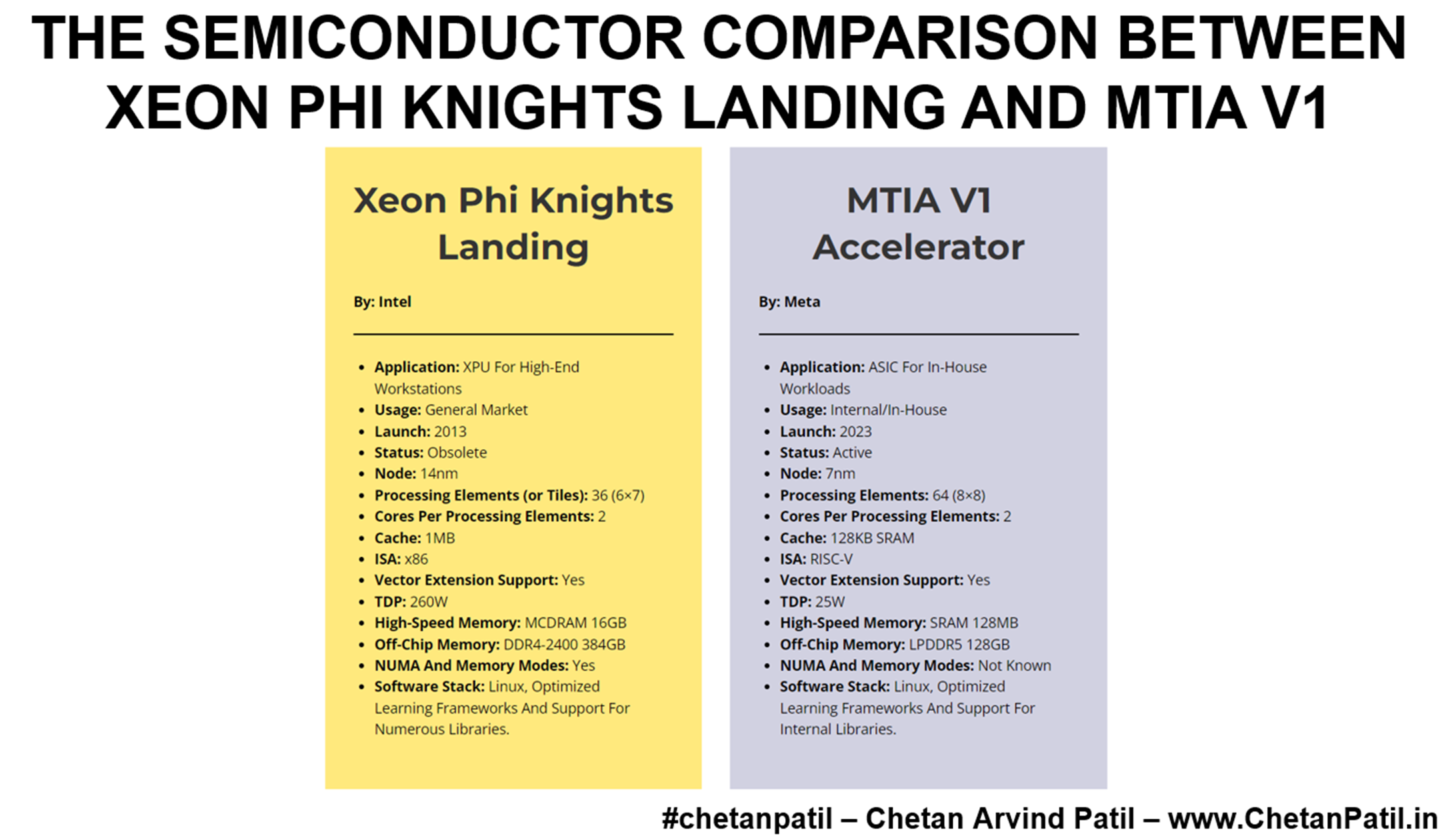
In 2010, Intel launched a new architecture-based solution for the high-end workstations. Codenamed Intel Xeon Phi Knights Ferry. It was a co-processor that would allow faster processing and training due to the massively parallel thread and memory level optimization with the help of multiple cores sharing high-end channels and memory. The technology node used was 45nm.
Over the next few years, Intel iterated on the design and launched Knights Corner with 22nm, followed by Knights Landing with 14nm. Knights Landing was a breakthrough architecture, allowing operating systems and applications to run on the architecture itself and eliminating the need to off-load and train. On top of this, the rich set of system and software-level architecture support from Intel and the Open Source community made it easy to use.
On the architectural level, it provided an elegant way to handle threads by using processing elements coupled with powerful but power budget-friendly cores and the ability of vector processing.
On the memory front, the Knight Landings used NUMA and memory modes to speed up the data training. There were supercomputers and data centers that started to utilize this architecture, and, to date, they still do – Tianhe-2 is one such supercomputer.
All these features created a lot of buzzes and focused on Xeon Phi Knights Landing, a breakthrough architecture to compete against the GPU leaders. However, the subsequent few launches of this architecture were supposed to be with sub-10nm, which unfortunately did not go as planned.
Even then, the Xeon Phi series set introduced a new way to stack the cores and package them on a chip. The key was the processing elements (a.k.a Tiles) organized in a grid manner and a combination of high-bandwidth memory that could act in different modes to further speed up the end applications.
Flashback to 2023, Meta launched an accelerator called MTIA V1. It is designed for their in-house workload requirements and will also get deployed in the supercomputers and data centers Meta will run. Though it is not an XPU, it can speed up the applications by focusing on instruction, memory, and thread-level parallelism.
However, after reading through the available details around this MTIA V1. The inspiration for this architecture is, indeed, now obsolete, Intel Xeon Phi Knights Landing.
It is evident not only based on how closely the feature sets are but also the way the MTIA V1 uses architectural features like combining two cores into one processing block and making use of vector support to enable the ability to run multi-threading on the processing elements by utilizing the high-speed cache and lower level memories.
The major differentiating factor between the two is the technology node and how it impacts the TDP. Besides this, MTIA V1 is comparable with Intel Xeon Phi Knights Landing.
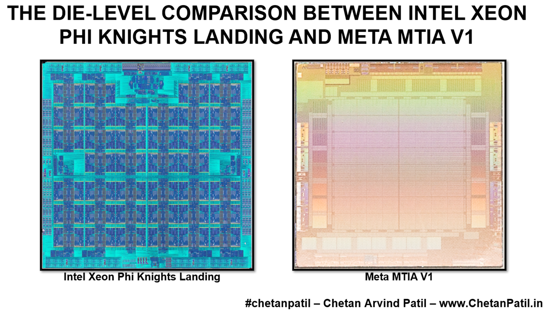
Even at the die level, the comparisons show the blocks are placed similarly, including the connections from processing elements to the memory and different interconnections.
This comparison shows that several new AI-focused accelerators and custom chips are looking back at the old designs and improving those for internal requirements. The major innovation is mainly on the software to architecture mapping rather than the architecture itself.
This approach will extend to architecture design (chiplets) more optimized for the AI workloads. It leads to whether these are breakthrough architectures or inspired architecture packaged with new technology nodes and better software mapping solutions.
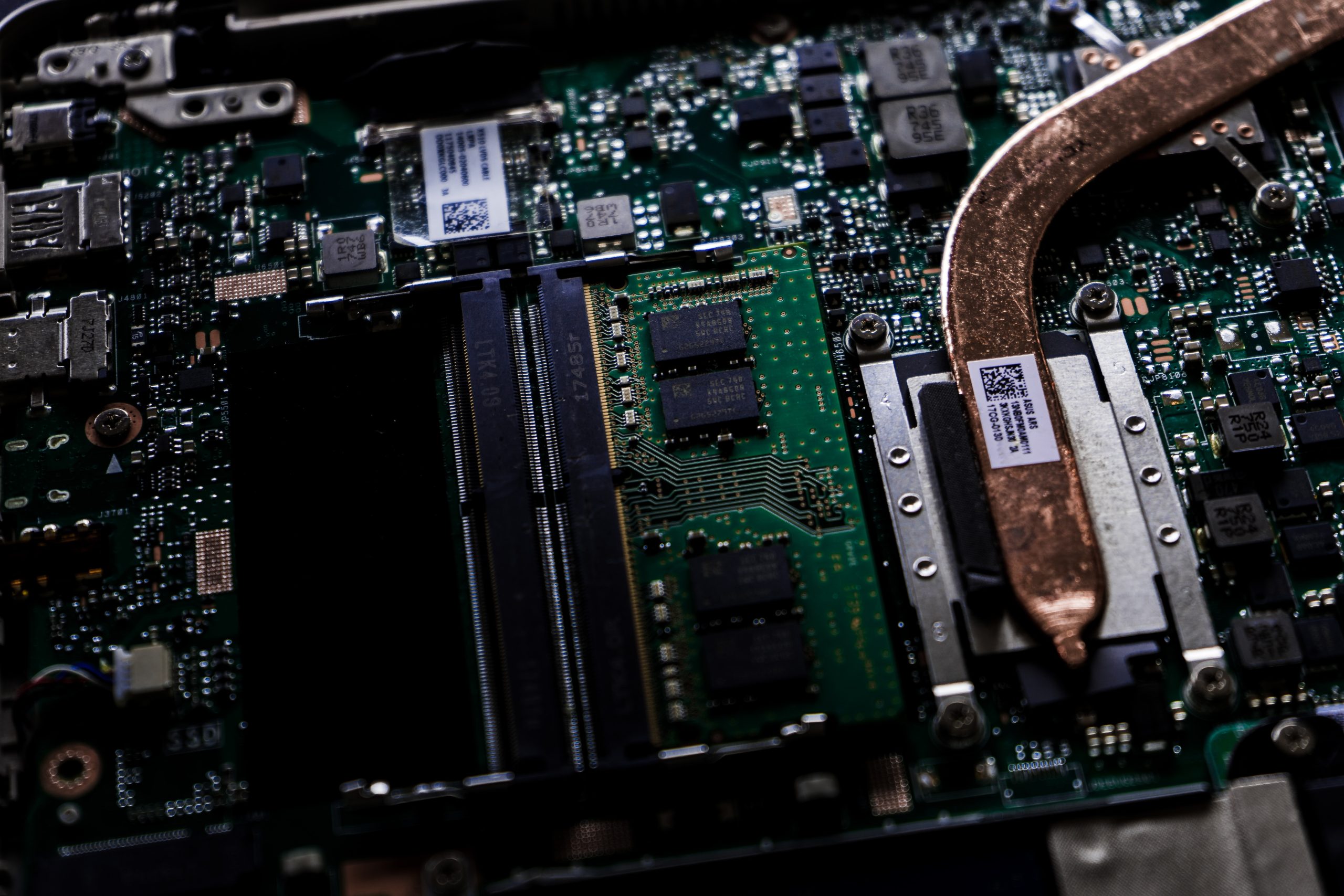
In computer architecture, computing (compute), memory, and interconnect are the three main components of a computer system and are thus critical in CPU, GPU, and XPU design. These three pillars determine the speed and efficiency of the system. The faster these three blocks are, the faster the system can run programs and perform tasks.
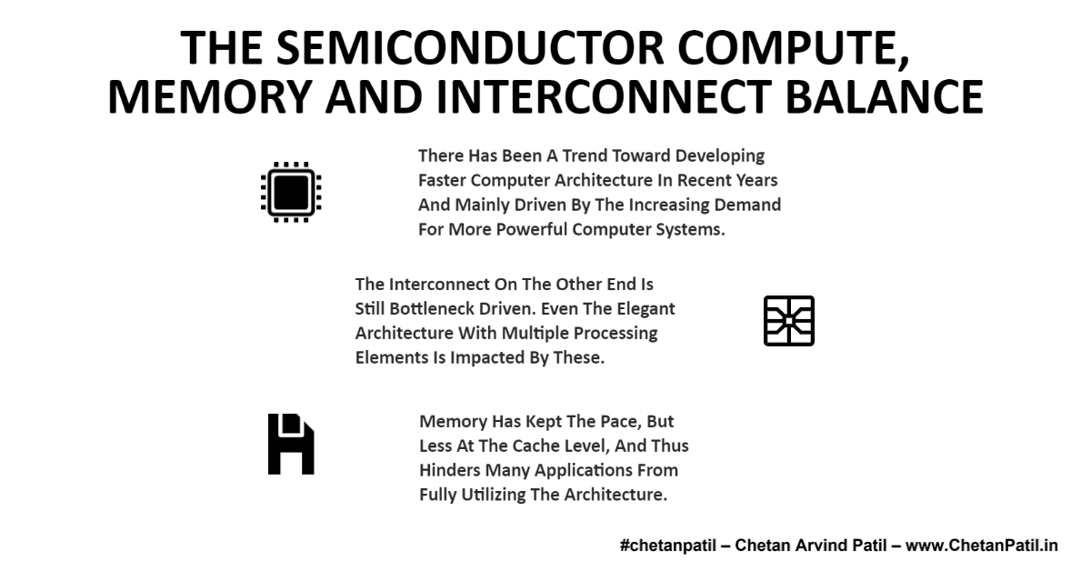
There has been a trend toward developing faster computer architecture in recent years and mainly driven by the increasing demand for more powerful computer systems. A speedier system helps improve the computer system’s performance by allowing them to transfer data more quickly between the different components of the system.
Three Pillars:
Compute: The compute refers to the central processing unit (CPU), the computer’s brain. The CPU performs all the calculations and operations required to run a computer program.
Memory: Memory refers to the storage of data and instructions used by the CPU. Memory types: primary memory and secondary memory. Primary memory is located on the motherboard and is used to store the data and instructions currently being used by the CPU. Secondary memory is located on storage devices such as hard and solid-state drives and is used to store data and instructions not presently used by the CPU.
Interconnect: Interconnect refers to buses and wires connecting a computer system’s CPU, memory, and other components. The interconnect allows the CPU to communicate with memory and other members and is responsible for transferring data and instructions between the different parts of the computer system.
To achieve this goal, feature balance of compute, memory, and interconnect is a must-have.
Compute blocks have already expanded into different types of architectures. They range from CPU, GPU, and NPU to more ASICs. Memory has kept the pace, but less at the cache level, and thus hinders many applications from fully utilizing the architecture. The interconnect on the other end is still bottleneck driven. Even the elegant architecture with multiple processing elements is impacted by these.
Even though a lot of effort has gone into bringing harmony across these three XPU blocks, there still seems to be no end to the pursuit of achieving the desired goal, which is also evident from the fact that several AI-focused companies are going in-house to develop there own silicon chips that can drive the future workloads.
One of the fundamental reasons that general-purpose computing systems need to catch up is the ever-changing workload. In the past, most workloads were general-purpose applications such as word processing, spreadsheets, and web browsing. They required significantly less computing. However, in recent years, there has been a shift towards more specialized workloads such as artificial intelligence (AI), machine learning (ML), and data analytics.
These specialized workloads place different demands on a computer system’s computing, memory, and interconnect components. For example, AI and ML workloads require a large amount of computing power, while data analytics workloads require a large amount of memory.
The changing workload is forcing CPU, GPU, and XPU designers to rethink how they design these systems. Designers are now looking for ways to improve the performance of these systems for specialized workloads.
One way designers improve CPU, GPU, and XPU performance for specialized workloads is by using heterogeneous computing. Heterogeneous computing is a technique that uses multiple types of processors to perform a task. For example, a system might use a CPU for general-purpose tasks and a GPU for AI and ML tasks.
Another way designers improve CPU, GPU, and XPU performance for specialized workloads is by using specialized hardware. Specialized hardware is hardware that is designed specifically for a particular task. For example, there are specialized hardware accelerators for AI and ML tasks.
Whichever way the computer architect will go. There is no end to the continuous focus to bring the perfect balance across computing, memory, and interconnecting. The research and development activities around these blocks will always continue to find the flawless balance of the three critical pillars of any XPU system.
The applications that run on silicon architecture are constantly evolving. Today, these architectures are more compute and memory intensive than ever before. It also means that the users of these applications are processing more data and thus demand the lowest latency possible.
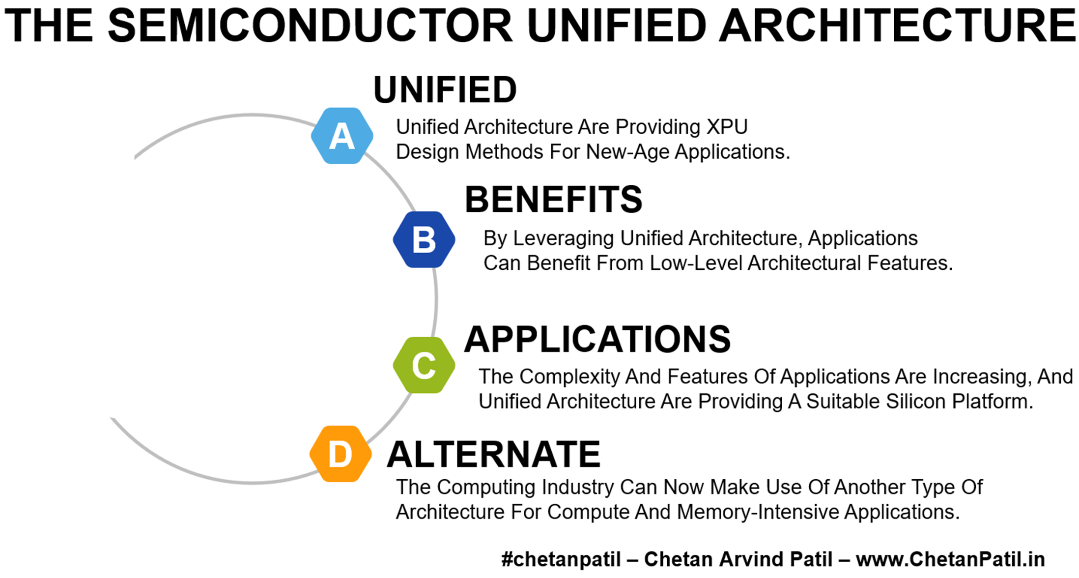
In reality, achieving good latency is challenging for any computer architecture. It is valid for CPUs, GPUs, specialized ASICs, and so on. Computer architects have been exploring a unified architecture to bridge the gap between higher user experience and lower latency. The goal is to connect different types of XPU blocks uniformly and thus allow the application to have faster memory access, which speeds up the computation.
Unified: Unified Architecture Are Providing XPU Design Methods For New-Age Applications.
Benefits: By Leveraging Unified Architecture, Applications Can Benefit From Low-Level Architectural Features.
Unified Architecture is more suitable for general-purpose computing, so high-bandwidth demanding applications still use Non-Unified Architecture. However, as the application complexity along with silicon design and manufacturing (chiplet) changes, a case in favor of unified architecture is being made.
At the application level, there can be contention with the use of unified memory. However, harmonious architecture can still provide better performance in terms of design and response time by using memory-level caching algorithms.
Companies already use unified architecture to build more powerful chips with better silicon areas. It can also improve the application performance by 2x to 4x. On another side, by better utilization of resources such as memory, bandwidth, and data, the overall cost of processing decreases, thus enabling better battery life and a higher user experience.
A computer architecture that follows a unified approach can get used for different computing needs, from gaming to science. It also reduces the response time of AI-driven applications, which are time-sensitive.
Applications: The Complexity And Features Of Applications Are Increasing, And Unified Architecture Are Providing A Suitable Silicon Platform.
Alternate: The Computing Industry Can Now Make Use Of Another Type Of Architecture For Compute And Memory-Intensive Applications.
By leveraging the benefits of unified architecture, the silicon industry is pitching a case against non-uniform architecture that has primarily dominated learning applications. However, it is still too early to say whether providing a single block of memory to different types of CPUs, GPUs, and NPUs will be the de-facto design process for laptop and PC SoCs.
Whichever way the computer architecture development progresses, computer architects have provided an alternative for the semiconductor computing industry by showcasing the power of unified architecture.
THE REASONS TO DEVELOP CUSTOM SEMICONDUCTOR CHIP IN-HOUSE
As technology is progressing and touching every aspect of day-to-day life, the dependence on semiconductor solutions is also growing. These solutions are often made by semiconductor companies and can power several things from sensors to a smartphone to cars to satellites to name a few.
One of the most critical infrastructures that the semiconductor industry powers are data centers and portable computing systems. These two systems are interconnected as one cannot do without the other. Today, majority of the request a smartphone users sends ends up in one of the numerous data centers around the world. The data centers then quickly crunch the request and send it back to the requesting user. As the customer base and internet users grow, there is a surge in demand for power-efficient computing systems (both data centers and portable computing systems) by the software or data-driven companies/industry.
Data-Driven Industry Is Getting Into Custom Semiconductor Chip Development
The big software and data crunching companies are often dependent on specific semiconductor solution providers who have been powering their data centers and portable computing systems for decades. The silicon chip these semiconductor companies design often falls in the category of the general-purpose chip, so the same is used by different customers even though their requirements might differ. So far, general-purpose strategy has worked wonders. However, as the software industry explodes (due to data), the big giants are realizing the importance of powering their data centers (and in some cases portable computing systems too) by developing custom chips in-house.
This change in landscape is mainly because the data crunching companies understand the need, purpose, and features that they require to drive bottleneck-free solutions for their customer. This can only be possible by starting chip development in-house so that software companies can deploy custom chip solutions across their data centers to drive services more efficiently. This is evident from the fact that YouTube has deployed its chip for video transcoding for faster processing of videos, and even Microsoft’s Pluton secure chip solution for its Windows platform.
While providing better solutions is certainly the main goal of developing the custom chip, there are several other reasons too. All these reasons ensure the in-house chip development by non-semiconductor companies is a win-win idea or not.
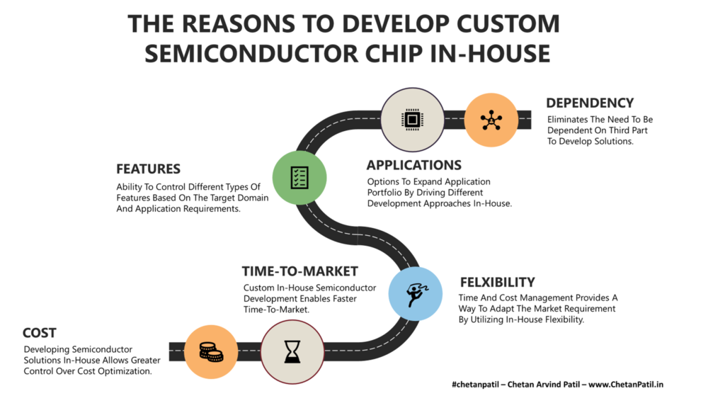
Cost: One of the major driving factors of developing chips in-house (at lead the designing part) is the cost. Having control over what chip needs to be designed and how to deploy it (as per the features) can potentially enrich user experience while bringing in savings. Savings are captured mainly in the form of usage when different computing systems within the company start utilizing the custom solutions. In many cases, the benefits can also be gauged based on how much power savings are achieved (data centers) compared to the traditional outsourced general-purpose solution.
Time-To-Market: Another benefit of designing custom semiconductor chips is for companies whose end product is a smart solution. This can range from kitchen appliances to television to desktops and many more. Having the ability to design and create chips in-house can allow greater control over launching products and takes away the uncertainty that general-purpose solutions provide. This is very true for data centers that heavily rely on x86 architecture solutions to drive future data centers.
Flexibility: Software changes very quickly and can demand new features out of the silicon chip. If there is no in-house development, then all these requests will eventually have to go out of the company in form of outsourcing. If there is a dedicated silicon development in-house team, then the software team can work in collaboration with the internal team (safeguarding IPs) to drive better hardware-software systems to power emerging solutions.
Features: If a company is selling laptops and relies on an outside vendor for chip development, then it makes them vulnerable due to dependency. Incorporating chip development in-house can provide a way to balance the chip requirement that can drive better systems. This can also push outside vendors to bring new features and in the long term, the competition helps the industry at large.
Applications: Developing in-house semiconductor chips can also provide avenues to expand the application area. This can be very true for smart device providers who often have to build systems based on what is available in the market. In-house chip development activities if planned well can allow companies to expand their portfolios by driving new end-products for their customers.
Dependency: Companies that are into data centers are heavily dependent on different companies for silicon chips to power their systems. Many of these solutions are not specifically designed to cater to everyone procuring the company’s request. This makes the data center companies heavily reliant on external factors to driven in-house innovation which today certainly requires custom chips.
All of the above reasons are the driving factor that is pushing several big software companies to drive in-house semiconductor chip development plan.
It is also true that not all companies have the need or focus to create such custom solutions. But in the long run, as the dependency on the silicon chip grows, the risk associated with not developing an in-house semiconductor chip might be far greater than not planning for it.
THE REQUIREMENTS TO DEVELOP CUSTOM SEMICONDUCTOR CHIP IN-HOUSE
Developing semiconductor solutions is not an easy task. Even for big software giants, it has taken years of planning and execution to come to a stage where they can deploy custom in-house developed silicon solutions across data centers and portable computing systems. This is why it is important to understand the different requirements that are the driving factor in ensuring the in-house semiconductor chip is impactful and profitable at the same time.
In-house silicon chip development requirements do take time to execute and often require tons of resources apart from the time it takes to perfect a semiconductor chip solution.
Team: The most important criteria for developing a successful in-house chip is to ensure that there is a team with an excellent set of skills to execute custom chip development flawlessly. The team often has to be a combination of excellent design and manufacturing skills. This means hiring individuals who have been in the semiconductor industry for a long time and are capable of developing semiconductor solutions via long-term research and development. A dedicated manufacturing team is also critical to bring ideas to life.
Acquisition: The team is one part of the development of in-house silicon chips. Another part is the ability to ensure that the company can acquire outside assets (IPs and patents) as and when required. This greatly pushes the in-house development activity in a positive direction and many cases reduce the efforts required to bring in-house silicon chip development to reality.
Investment: Managing teams, labs, and other resources often require a massive amount of money. If a company without a semiconductor background is entering in-house chip development activity, then the company should ensure there is a large amount of investment available for a very long time. This is why it is important to ensure that over the long period of chip development process and research, the investment activity will pay off in the long run.
Roadmap: In-house chip development also means having a clear strategy as to why the company should do it. Having teams and resources to tackle one specific feature without a plan is not a good strategy to invest time and money behind in-house chip development. Major emphasis should be on the long-term plan and how it will benefit the company. This often requires a clear roadmap is a must-have requirement.
Balance: Not all semiconductor solutions require in-house development, and that is why it is very important to balance the focus in terms of what part of the silicon requirement should be outsourced and which is worth developing in-house. It is not possible for software or data-driven companies to become full-fledge semiconductor solution providers overnight and no single company (even core semiconductor) develops everything in-house. This is why a filtering mechanism of balancing the in-house and outsourcing is important.
Bottlenecks: Major criteria of in-house development of silicon chip is also to remove any barrier in developing new products. The roadmap should allow bottleneck-free development of in-house semiconductor products as long they meet the company’s requirements.
The reasons and requirements showcase how and when the non-semiconductor companies should get into the semiconductor design segment. In-house semiconductor development has already started long back and many of the companies (Google, Microsoft, and Amazon to name a few) have already enjoyed success around it. The major reason for doing so has been the greater control of designing features that in reality removes the issues the companies were facing.
This trend of taking things in hand and designing solutions in-house is certainly going to continue, more so due to the semiconductor shortage and the impact it had on several industries.
Every software application eventually has to get executed on a hardware system. Whether the software application is running on a smartphone or a data center, the data processing request has to get decoded (binary instructions) before the hardware system can process the request successfully. This seamless exchange of processes between software and hardware forms the base for a computer system.
Software form factor, user interface, and the speed might have changed over the years. However, the need to have a processing unit that can execute all the software code has not. Over the last two decades, the de-facto processing unit – the Central Processing Unit (CPU) – has seen several semiconductor and computer architecture backed technological advancement, that has taken computing to the next level.
As the software layers (application, presentation, session, and transport) are becoming model-driven (more pro-active, than re-active), so is the need to process the unique data/compute/memory intensive requests at the hardware-level.
Traditional CPU earlier was designed to handle a single request at a time. Then, the computing world moved towards multi-CPU (multi-cores) to cater to the parallel computing demand. Today, the de-facto is a System-On-A-Chip (SoC) that packs the CPU, the Graphics Processing Unit (GPU), and other processing units to process the high-resolution, high-speed, highly-data intensively requests in the shortest possible time.
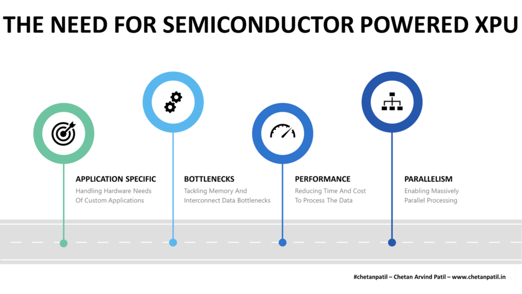
Semiconductor Powered XPU (X Processing Unit) Are More Application-Specific Than General-Purpose
The integrated system (mainly CPU + GPU on an SoC) has not been able to keep up with the computing world’s data processing demand. It has pushed the computer architects to design new types of processing units (apart from high-bandwidth memory, cache coherence, and smarter interconnect topology) that are more application-specific than general-purpose.
This race to come up with the new type of processing units has given rise to XPU:
X = Application Domain — Vision, Graphic, Neural, X-Reality, Video, Audio, and so on
P = Processing
U = Unit
XPU is different than CPU and GPU as it caters to the specific needs of the application. XPU is more application-specific, and it can work standalone or as a co-processor/co-unit alongside the CPU and GPU. XPU is geared towards throughput and speedy data management that takes the best out of the CPU and GPU design methodology to enable application-specific needs. XPU is not only Application-Specific Integrated Circuit (ASIC) due to the workload it is designed to cater to, but can also be classified asApplication-Specific Standard Product (ASSP).
The rise of XPU is enabling a new era in computing. The hardware and the semiconductor market are enjoying different challenges and solutions the XPU brings. Intel is betting big on it, and so is AMD. Apart from these two semiconductor giants, there are numerous innovative startups (and academic research) that have XPU powered solutions and are pushing the computing industry towards next-gen data processing.
Several types of XPU are available. It is vital to understand how these differ from each other apart from the two processing giants – the CPU and the GPU.
There are numerous XPU powered examples in the market. Many of these are still in a nascent stage and yet to prove the solution in the market. Given the growth and demand for new AI workloads, the XPU catalog will keep growing.
Below are the major semiconductor powered XPU:
AIPU – AI Processing Unit — AIPU is targeted towards an Artificial Intelligence solution and is mainly designed to cater to the Edge AI market. MediaTek Helio series of SoC is an example of AIPU integrated with CPU and GPU. Even RAIP – Real AIProcessing Unit (RAIPU), IPU – Intelligence Processing Unit or Image Processing Unit, EPU – Emotion Processing Unit – fall under IPU with the only difference being the change of name. The goal of AIPU, RAIPU, EPU, and IPU is the same – to process data to make a decision that is at-level or at-part with human intelligence.
APU – Accelerated Processing Unit — APU design requires fusing the CPU and GPU into a single die. AMD’s A-Series processor is a perfect example of an APU. APU is also capable of running a heterogeneous system by utilizing system-level architecture and software features.
AMPU – Analog Matrix Processing Unit — AMPU is designed to cater to the data training needs that are often large parameters that execute multiple matrix multiplications. AMPU custom feature to handle such parameters and matrix operations allows speedy training without relying on the external memory. MYTHIC’s Analog Matrix Processor is an example of AMPU.
BPU – Brain Processing Unit — BPU is envisioned to minim the human brain as it is. The processing unit is capable of performing multiple TOPS. Horizon’s Journey line of products is considered the first BPU ever and is designed in close collaboration with the Baidu Institute of Deep Learning. BPU may also form the base for Level 5 automation.
CPU – Central Processing Unit — CPU is the de-facto processing unit and is vital for general to specific purpose computing needs. Intel and AMD are leading the CPU innovation along with ARM. CPU is here to stay and will keep providing the much-needed multi-tasking capability for consumer applications. On top, Academia is still engaging in research to make cache and data pipeline more energy efficient.
DPU – Dataflow Processing Unit | Data Processing Unit | Data Parallel Unit — DPU focuses on speeding up the data movement between the cores and the memory. It requires a new interconnect topology apart from the smart placement of sub-blocks to minimize bottlenecks. The instruction set allows for faster memory and compute-intensive processing. Intel already several RISC (AVX512) instructions set to optimize processing for x64. DPU takes it to the next level with its highly optimized data pipeline, which enables massive parallelism. Fungible’s DPU is one such example apart from Deep Vision’s ARA series. RDPU – Reconfigurable Dataflow Processing Unit – is also a type of DPU.
DLPU – Deep Learning Processing Unit — A DLPU finds similarity with DPU. It is a domain-specific solution to enable faster training. DLPU finds use in Edge AI and similar applications. Researchers first showcase DLPU with DianNao paper, and recently in Cambricon-F paper.
GPU – Graphics Processing Unit – Like CPU, GPU has been in the market for a long time and is designed to cater to graphics applications. In the last few years, GPU has also found its way into AI/ML/DL applications too. Highly parallel design (with multiple core and large memory) of GPUs enables faster computation. GPU’s efficient programmability also allows faster training of dataset. NVIDIA by far is the leader in the GPU domain along with AMD, which is not far behind. Depending on how the GPU is fabricated in the computer system, it also gets classified as = DGPU – Discrete Graphic Processing Unit, GPGPU – General Purpose Graphic Processing Unit, EGPU – External Graphic Processing Unit, IGPU – Integrated Graphic Processing Unit.
HPU – Holographic Processing Unit — Coming out of Microsoft, HPU is designed for X-Reality. It incorporates design to process rich information that is generated by the sensors and cameras on the X-Reality device. HPU incorporates processing units to implement DNNs.
MCPU – Micro Controller Processing Unit — MCPU is not used to run operating systems or frameworks, but instead are geared to run Real-Time Operating System (RTOS) powered solution. MCPU find use in automotive, remote devices and even laptops desktop to offload non-critical tasks. ARM, Texas Instruments, and others have been providing MCPU solutions for a few decades. In the AI-powered world, the solution around MCPU is increasing, and architecture design is adapting to it.
NPU – Neural Processing Unit — NPU implements all the required blocks to enable faster data modeling using neural networks. Alibaba’s Ali-NPU is one such example. There are different types of NPU: NDPU – Neural Decision Processing Unit, NNPU – Neural Network Processing Unit, NDPU – Neural Decision Processing Unit. Eventually, the end-goal of the types of NPUs is the same – train the data faster using a neural network and framework.
QPU – Quantum Processing Unit — QPU is a computational unit that uses quantum computing principles to perform a task. The physics used in QPU is drastically different than the general-purpose CPU. D-Wave Systems is the leader in QPU, and their QPU follows superconducting computing. Google, IBM, and Intel have QPU based on a quantum circuit. QPU is massive and not designed for mass-market and are supposed to compete against AIPU.
SPU – Streaming Processing Unit — SPU is useful to process streamed data. The structured data enables placing the cores and memory to minimize the delay in bringing the new data to process. Google’s TSPU – Tensor Streaming Processing Unit – is an example of SPU. There are different types of SPU available in the market apart from TSPU: GSPU – Graph Streaming Processing Unit, TMPU – Texture Mapping Processing Unit, TPU – Tensor Processing Unit
VPU – Vision/Visual/Video Processing Unit — VPU is coming out in the market due to the demand for providing a rich visual experience. VPU consists of more video encoding and decoding units to enabled faster 3D processing. X-Reality is an application area where VPU finds use. Intel’s Movidius VPU is a perfect example of how to use processing units to process video applications with low-latency.
XPU is unique and solves niche problems. The challenges that come with it are many. Below are the hurdles and challenges that the semiconductor powered XPU face:
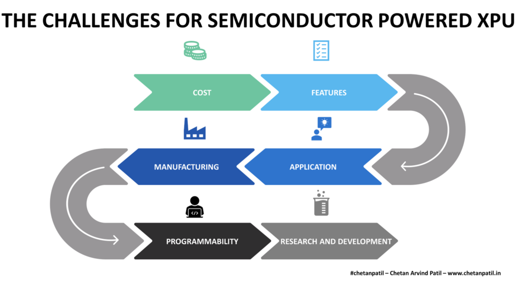
Cost: Designing a new processing unit not only enables new features to run the workload in the most optimized way possible. But it also adds the cost of design, development, and manufacturing. Balancing the CapEx is always the de-facto goal of any organization, and in the case of XPU, the stakes are higher given the stiff market competition. Companies looking to come out with more XPU based designs and solutions will have to make the process cost-effective to breakeven faster.
Features: XPU is feature-specific. Deciding which problem the XPU is going to solve is difficult to find. The semiconductor industry has launched different types of XPU that cater to almost all the possible computing domains and problems possible. Upcoming XPU will have to beat the existing XPU not only from the design point of view but also with respect to the features that make the new XPU sustainable in terms of power, performance, area, and cost.
Application: Defining use cases and features for XPU is another challenge. It requires figuring out the bottleneck in the existing applications/workloads and then designing the solution at the silicon level to solve it. TSU is one such example, which removes the bottleneck to train the data. Such a unique feature-based XPU is going to make it stand out in the market.
XPU Will Drive Innovation Along With General-Purpose Processing Units
Manufacturing: XPU either needs to be fabricated along with the CPU or as another block with the CPU inside the SoC or as a separate co-processing unit. In any of the three cases, it takes a unique semiconductor manufacturing process to ensure there is no process, quality, package, and reliability issues. Multi-Die Multi-Chip powered chiplets can be one way to ensure future XPU designs for manufacturability. The technology node and the packaging technology needs to be thoroughly tested before making the XPU with it. The goal of reducing the cost of manufacturing for XPU will be another challenge.
Programmability: Hardware is designed to run the software. Developing and running applications on any piece of silicon (mainly those designed to run operating systems and frameworks) requires the support of system-level libraries to ensure the data being processed can make use of all the internal features. Semiconductor companies developing different types of XPUs will have to provide APIs and system-level hardware interface libraries. This requires time and cost to develop. To keep developers engaged dedicated continuous API development teams are required. Providing such software features is vital and also a challenge to the XPU design team.
Research And Development: Continuous R&D is a vital factor that leads to a new type of XPU. It is critical to ensure that the R&D team can collaborate with academia to innovate new processing blocks. Organizing a dedicated top-notch R&D team is still a challenge given the competition in the semiconductor industry. Investment is another differentiating criteria when it comes to advancing new XPU designs.
It is an exciting time to be in the XPU domain. General-purpose CPU and GPU are here to stay, and along with XPU will enable a new, powerful and efficient way to solve the data problems.
However, the need to innovate in the competitive semiconductor industry will be the race to watch out. Companies like Intel, Apple, AMD, Microsoft, Google, Amazon, and Facebook will play a crucial role in pushing the market for semiconductor powered XPU solutions, alongside promising FAB-LESS startups worldwide.


@QHL6_DSCx7@5x.jpg)