Photo by Denny Müller on Unsplash
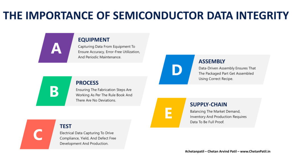
THE IMPORTANCE OF SEMICONDUCTOR DATA INTEGRITY
The semiconductor industry has been utilizing data to drive design and manufacturing for a very long time. The reason is the high cost and penalty of manufacturing a product without thoroughly reviewing the semiconductor data.
The growing importance of data is the primary reason why the semiconductor industry has always found ways to capture data cleanly. Capturing relevant data has helped semiconductor design and manufacturing. However, as the reliance on semiconductor data grows, it is crucial to implement end-to-end data integrity.
Semiconductor Data Integrity: How accurate, complete, and consistent semiconductor product-related data is.
Data integrity questions arise in the semiconductor (and several other industries) industry when for any given process steps or product, there are parts of the data that are missing or not traceable. Such miss-steps can occur when there is a need to go back and look at the historical data to capture any deviations that might in the future lead to re-calls (a process that the automotive industry has mastered and deployed for decades) to avoid failure in the field.
There are specific sub-steps in the semiconductor product development (mainly the manufacturing side) process that should be compliant from a data integrity point of view.
Equipment: Advanced equipment gets used for semiconductor testing, validation, and manufacturing. Capturing the data correctly and accurately is key to validating the product behavior. Any miss-steps causing data integrity issues can lead to an incorrect decision which can eventually cause losses in terms of revenue and time.
Process: There are thousands of steps that every semiconductor chip has to follow during the fabrication stage. Data is the only way to validate whether the process steps (lithography, etching, etc.) got successfully executed. If the data is missing or not correctly captured, then a faulty product will get fabricated.
Test: Electrical data during the post-silicon stage is required to validate the compliance aspect of the product development apart from capturing yield trends/issues. Data integrity during electrical testing is vital in driving accurate conclusions. An incorrect assumption or analysis (due to inaccurate data) can have negative consequences during the production phase.
Assembly: Assembly data integrity is vital as it is the final stage of any manufacturing process. After assembly, the parts get delivered to the customers. Any last-minute data points that can alert the manufacturing houses of possible issues can eventually save thousands of dollars apart from saving time. Hence, data needs to be accurate and compliant.
Supply-Chain: Balancing the inventory with market demand is a vital part of the semiconductor industry. Doing so requires relying on market intelligence. Thus the data provided by the market intelligence tools should be error-free. Hence, data integrity also applies to the data-driven supply chain.
Above are the handful of areas where the semiconductor data integrity is applicable by default. There are still specific steps that semiconductor companies/industry needs to revisit to ensure that product that goes out in the market has end-to-end data integrity.
In the long run, applying data integrity to semiconductor product development provides a positive impetus for the semiconductor industry/company. On top of that, it pushes them to produce more critical products for a wide range of industries apart from enabling customers with information about any data points that can have both negative and positive impacts on semiconductor products.
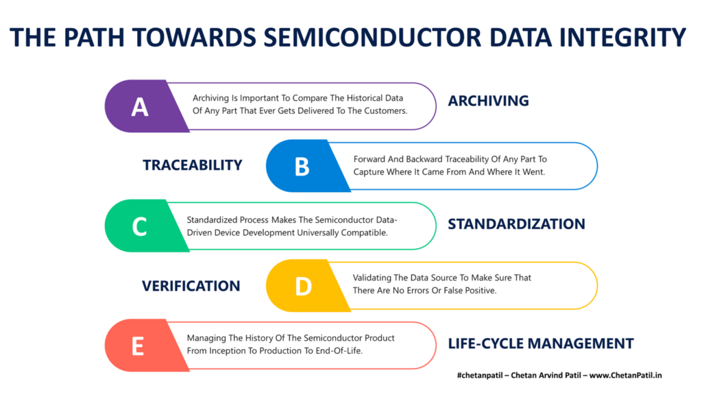
THE PATH TOWARDS SEMICONDUCTOR DATA INTEGRITY
An efficient semiconductor product development process requires semiconductor data integrity and should be a default feature. Otherwise, the semiconductor data collected and analyzed can lead to incorrect decisions that can severely impact the new product launch.
Over the last decade, several new data solutions have taken the process of semiconductor device design and manufacturing to a whole new level. However, there are still opportunities to apply data integrity around specific steps. Doing so will raise the bar of the semiconductor company deploying data integrity features, as it will encompass an error-free process.
Archiving: Long-term storage of semiconductor data should be the first and foremost goal of any semiconductor company. Faster storage and retrieval drives efficient data analysis to capture different features of a given product. There is a need for default features to validate the archiving process to capture gaps or missing data points. Such features will ensure any data retrieved in the future will be reliable, completed, and accurate. Thus data integrity needs to be a default part of archiving process.
Traceability: Traceability allows connecting the data to a specific product. Billions of semiconductor products get shipped out every year, and it is critical to capture every actionable data a given semiconductor product generates. It demands a unique and robust traceability process so that the data can be correctly connected to the right product, thus driving next-gen data integrity in the semiconductor. Several approaches are already present, and as more products get shipped out, the importance of traceability will only grow.
Standardization: Semiconductor industry has several standards it follows diligently. However, it is important to keep revisiting these standards to ensure that the latest learnings from different semiconductor companies (and processes) are applied. It will drive further make the standardization processes more robust. The semiconductor industry should also focus on data standards by bringing more efficient data formats that are easy to store, parse, use, and analyze. All this can ensure end-to-end data integrity.
Verification: Data generation is half job done. It is also vital to verify the data generated. Cross-checking, validating properties, questioning data, and analyzing are keys to ensuring the semiconductor data is 100% compliant and is accurate. Moving forward, semiconductor companies relying on data analysis will have to by default deploy data verification techniques to capture any anomaly, thus avoiding miss-information and driving data integrity by default.
Product Life-Cycle Management: Product life-cycle management software tools have been around for decades. Cloud-driven solutions have also positively impacted product management, mainly the bill of material. However, slowly these software tools are becoming complex. Complexity makes the process error-prone and can lead to inaccurate information, thus affecting the data connected with the product. PLM tools will have to evolve and produce simple, minimal, and robust solutions that minimize human efforts and maximizes efficiency by keeping data integrity at the center stage.
The majority of the above points are already in place but are becoming complex due to the increasing semiconductor data (along with products) year on year. Managing data without losing its integrity should be the default focus of the semiconductor data solutions provider and users (semiconductor companies). Any missing points or issues at the source can invite confusion in the future. Hence, capturing and solving the gaps at the first step should be the goal of semiconductor data tools.
The semiconductor data integrity will also be a key for the emerging semiconductor FAB-LESs and FABs. It certainly requires investing in the new semiconductor data handling process. In the long run, it also implies that the demand for talents with data skills for the semiconductor industry will keep increasing.