Category: DESIGN

  • The Need For Silicon To Become Self-Aware

    Image Generated Using DALL·E


    What Is Silicon-Aware Architecture

    As chips approach atomic dimensions, every region of silicon begins to behave differently, shaped by fluctuations in voltage, temperature, stress, and delay. Traditional design methods still rely on fixed timing corners and conservative power margins, assuming stable and predictable behavior.

    At three nanometers and below, this assumption breaks down. Modern workloads in artificial intelligence, edge computing, and automotive systems operate under constantly changing physical and electrical conditions. To sustain both performance and reliability, silicon must evolve beyond precision into perception. It must know its own state and react intelligently to it.

    A silicon-aware architecture is the structural basis for this evolution.

    It represents a chip that not only executes logic but also perceives its own electrical and physical behavior in real time. Embedded networks of sensors, telemetry circuits, and adaptive control logic create continuous feedback.

    The chip measures temperature, voltage, and aging, interprets the data internally, and fine-tunes its operation to maintain stability and efficiency. In doing so, the silicon transforms from a passive substrate into an active, self-regulating system capable of sustaining peak performance under diverse and unpredictable workloads.


    Adapting To Workload Reality

    Artificial intelligence workloads have redefined how silicon is stressed, powered, and utilized. Unlike conventional compute tasks that operate within predictable instruction flows, AI inference and training involve highly dynamic activity patterns. Cores experience extreme bursts of power consumption, rapid switching between memory and logic, and localized thermal buildup.

    These workloads create transient peaks in current density that can exceed traditional design margins by several times. A static chip designed with fixed voltage and frequency limits cannot efficiently manage such fluctuations without wasting energy or compromising reliability.

    Adaptive FunctionChallenge In AI WorkloadsTraditional LimitationSilicon-Aware Advantage
    Thermal RegulationLocalized hotspots in dense compute clustersGlobal throttling reduces overall throughputLocalized sensing and targeted bias control
    Power DeliveryRapid current surges during tensor operationsStatic voltage rails with limited responseOn-die regulation based on real-time telemetry
    Reliability AgingHigh stress cycles on interconnects and transistorsStatic lifetime deratingPredictive control extending operational lifetime
    Workload DistributionUneven utilization across coresCoarse scheduling by firmwareAutonomous, per-region load balancing

    A silicon-aware architecture introduces a path forward by allowing the chip to interpret its own activity and respond within microseconds.

    Through embedded sensing networks, the chip continuously monitors voltage drop, temperature gradients, and switching density. This information feeds local control loops that modulate power delivery, clock speed, or logic bias according to instantaneous demand.

    For AI accelerators and heterogeneous SoCs, this means that compute islands can self-balance, with one region throttling while another ramps up, maintaining efficiency without intervention from system software.

    In effect, silicon awareness enables the chip to become an adaptive substrate. Instead of relying on external management firmware to react after performance loss, the chip learns to anticipate workload transitions and adjust preemptively.

    This is particularly vital in AI systems operating near thermal and electrical limits, where efficiency depends not only on algorithmic intelligence but also on the chip’s ability to interpret its own physical state in real time.


    Barriers For Silicon-Aware Architecture

    The vision of silicon-aware architecture is compelling, but achieving it introduces significant design and manufacturing challenges. Embedding intelligence into the wafer adds power, area, and verification overhead that can offset the performance gains it seeks to deliver.

    The first barrier is integration overhead. Thousands of on-die sensors and control loops must fit within already congested layouts. Each additional circuit increases parasitic load and consumes power, limiting scalability.

    The second is data complexity. Continuous telemetry from large SoCs produces massive data volumes. Without localized analytics, monitoring becomes inefficient and costly.

    A third is trust and validation. Adaptive behavior complicates deterministic verification and safety certification. Establishing reliability for self-adjusting chips requires new design and test methodologies.

    Overcoming these challenges will require tighter co-design between architecture, EDA tools, and foundry process technology.


    Can True Self-Awareness Be Achieved

    Accurate self-awareness in silicon is an ambitious goal, yet the path toward it is already visible.

    Current SoCs employ distributed sensors, adaptive voltage scaling, and machine learning–assisted design tools that enable limited self-monitoring and optimization. These early steps show that awareness is not theoretical but a gradual evolution built through necessity. Each generation of chips adds more autonomy, allowing them to measure, interpret, and respond to internal conditions without human control.

    Achieving full awareness will require chips that can learn from their own operating history and refine their behavior over time. Future architectures will merge sensing, inference, and adaptation at the transistor level, supported by AI-driven design and real-time feedback from the field.

    The result will be silicon that maintains its performance, predicts degradation, and evolves throughout its lifetime, marking the shift from engineered precision to actual cognitive matter.


  • The Semiconductor Dual Edge Of Design And Manufacturing

    Image Generated Using DALL·E


    Semiconductor leadership comes from the lockstep of two strengths: brilliant design and reliable, high-scale manufacturing. Countries that have both move faster from intent to silicon, learn directly from yield and test data, and steer global computing roadmaps.

    Countries with only one side stay dependent, either on someone else’s fabs or on someone else’s product vision.

    Extend the lens: when design and manufacturing sit under one national roof or a tightly allied network, the feedback loop tightens. Real process windows, such as lithography limits, overlay budgets, CMP planarity, and defectivity signatures, flow back into design kits and libraries quickly. That shortens product development cycles, raises first pass yield, and keeps PPA targets honest. When design is far from fabs, models drift from reality, mask rounds multiply, and schedules slip.

    In all, semiconductor leadership comes from the lockstep of two strengths: brilliant design and reliable, high-scale manufacturing.

    Countries that combine both move faster from intent to silicon, learn directly from yield and test data, and steer global computing roadmaps. At the same time, those with only one side remain dependent on someone else’s fabs or someone else’s product vision.

    A nation strong in design but weak in manufacturing faces long debug loops, limited access to advanced process learning, and dependence on external cycle times. A nation strong in manufacturing but with a focus on design, the light industry depends on external product roadmaps, which slows learning and dampens yield improvements. The durable edge comes from building both and wiring them into one disciplined, high-bandwidth, technical feedback loop.

    Let us take a quick look at the design and manufacturing lens from country point of view.


    The Design

    A strong design base is the front-end engine that pulls the whole ecosystem into orbit. It creates constant demand for accurate PDKs, robust EDA flows, MPW shuttles, and advanced packaging partners, shrinking the idea-to-silicon cycle. As designs iterate with honest fab feedback, libraries and rules sharpen, startups form around reusable IP, and talent compounds.

    MechanismEcosystem Effect
    Dense design clusters drive MPW shuttles, local fab access, advanced packaging, and testJustifies new capacity; lowers prototype cost and time
    Continuous DTCO/DFM engagement with foundriesFaster PDK/rule-deck updates; higher first-pass yield
    Reusable IP and chiplet interfacesShared building blocks that accelerate startups and SMEs
    Co-located EDA/tool vendors and design servicesFaster support, training pipelines, and flow innovation
    University–industry, tape-out-oriented programsSteady talent supply aligned to manufacturable designs

    When design is strong, the country becomes a gravitational hub for tools, IP, packaging, and test. Correlation between models and silicon improves, respins drop, and success stories attract more capital and partners, compounding advantage across the ecosystem.


    The Manufacturing

    Manufacturing is the back-end anchor that turns intent into a reliable product and feeds complex data back to design. Modern fabs, advanced packaging lines, and high-coverage test cells generate defect maps and parametric trends that tighten rules, libraries, and package kits. This credibility attracts suppliers, builds skills at scale, and reduces the risk associated with ambitious roadmaps.

    MechanismEcosystem Wffect
    Inline metrology, SPC, and FDC data streamsRapid rule-deck, library, and corner updates for design
    Advanced packaging (2.5D/3D, HBM, hybrid bonding)Local package PDKs; chiplet-ready products and vendors
    High-throughput, high-coverage testProtected UPH; earlier detection of latent defects; cleaner ramps
    Equipment and materials supplier clusteringFaster service, spare access, and joint development programs
    Scaled technician and engineer trainingHigher uptime; faster yield learning across product mixes

    With strong manufacturing, ideas become wafers quickly, and learning cycles compress. Suppliers co-invest, workforce depth grows, and the feedback loop with design tightens, creating a durable, self-reinforcing national semiconductor advantage.


    A nation that relies solely on design or solely on manufacturing invites bottlenecks and dependency. The edge comes from building both and wiring them into a fast, disciplined feedback loop so that ideas become wafers, wafers become insight, and insight reshapes the next idea.

    When this loop is tight, correlation between models and silicon improves, mask reentries fall, first pass yield rises, and ramps stabilize sooner.


  • The Semiconductor Hurdles For Inspection

    The Semiconductor Hurdles For Inspection

    Photo by L N on Unsplash


    Semiconductor products often fail, and finding the root cause thus becomes a critical process. More so, when the product is already in production.

    Failure and root cause analysis are vital steps towards finding issues with the semiconductor product. Doing so requires an inspection process that allows engineers to look inside the chip.

    Several advanced equipment and technologies (SEM and beyond) can provide an in-depth view of what is happening inside the chip. The hurdles thus are not the availability of technology required to drive failure analysis. The real challenge is the complexity (silicon level) that the advanced design and manufacturing brings to enable failure analysis.

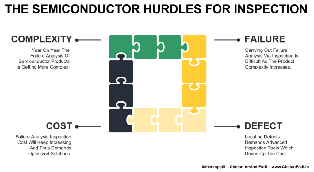
    Complexity: Growing transistor count increases the die level complexity, which brings difficulties to perform failure analysis without investing more than the required time, resources, and capital.

    Failure: During failure analysis (in the majority of the cases), it becomes difficult to narrow down the root cause for highly complex (3nm and lower) products. Advanced equipment does help, but not without investing a lot of time and cost.

    Overcoming different inspection hurdles is a vital step towards a fast resolution of why the product failed. At the same time, the growing design complexity of semiconductor products (coupled with different package technologies) is leading to constant upgrades of labs that enable such analysis and leading to the high cost of finding the defects in the product.


    Picture By Chetan Arvind Patil

    The fundamental process when carrying out failure analysis is the localization of defects. Doing so requires semiconductor products to run through several inspection steps, and it often requires looking at every layer. Biasing process helps, but it requires skilled engineers with years of experience to handle the inspection tools to find areas of concern within a given chip.

    Defect: Year on year, the localization of defects during the failure analysis is getting costlier and time-consuming. All of this leads to constant upgrades of equipment apart from the training of engineers.

    Cost: The cost of inspection to capture the failures is increasing due to the need to constantly upgrade labs apart from the time required to find defects in the highly complex products with advanced technology nodes. Solutions like do SEM are helpful but are also high on cost.

    Today’s advanced semiconductor product utilizing the latest technology node often comes equipped with billions of devices. Inspecting such devices is certainly not an easy task. More so, when the goal is to quickly root cause silicon-level issues.

    The importance of inspection as part of a semiconductor product (in case of failures) will only grow with the growing number of transistor counts. It is thus vital to focus on optimizing the process to perform failure analysis so that the operating cost is reasonable while also bringing skilled engineers who can efficiently carry out inspection-driven failure analysis.


  • The Growing Reliance Of Semiconductor Industry On Software

    The Growing Reliance Of Semiconductor Industry On Software

    Photo by ThisisEngineering RAEng on Unsplash


    Software is the backbone of several industries, including semiconductor. Several (maybe all) semiconductor activities cannot work without a software solution and are valid for several key stages like design, manufacturing, supply chain, and many more.

    This growing reliance on several stages is the primary reason it has become vital to utilize the best solution for all the stages of semiconductor product development. Doing so enables defect-free and error-free solutions for the end customers.

    The advancement in software tools has allowed the semiconductor industry to lower the time to market. As more advanced semiconductor technologies get deployed, the importance of developing faster and more accurate software will grow further and increase the reliance of the semiconductor industry on software solutions.

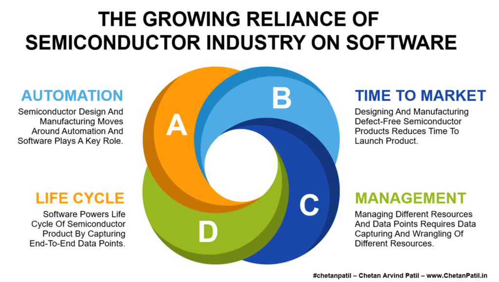
    Automation: Automated software solutions plays a critical role in capturing defects and errors during design or manufacturing stages.

    Time To Market: Software speeds the process of developing and launching semiconductor products. The reason is the ability to simulate and capture all the errors before products go to the customer.

    One key feature of the software is automation. It speeds up designing and also ensures defects get captured ahead of time. On another side, the software is powering the designing process of highly complex products without human interference.

    In the long run, such solutions may or may not work. However, raises questions of how much more software solutions can do (concerning design and manufacturing) and how it will impact the semiconductor industry.


    Picture By Chetan Arvind Patil

    Apart from semiconductor product development (design and manufacturing), the software also plays a vital role in semiconductor information management. It includes capturing and storing all the required data for a very long time.

    Software solutions around information and data management have been around for decades. However, the growing data complexity and the need to capture/process the data faster is leading bottleneck’s in the software solutions themselves. It has raised the demand for a new generation of software solutions to pull the information faster than ever.

    Management: Information management is a part of semiconductor product development and demands easy-to-use software solutions.

    Life Cycle: Managing product information demands long-term software-powered data storage and retrieval.

    As the need to reduce the time to market grows, the demand for software-driven automation will grow more. Semiconductor-focused software automation has been in place for several years. However, the market needs to enable new types of silicon products for the emerging market is demands novel ways to design and manufacture.

    All these requirements will further grow the reliance of the semiconductor industry on software and thus presents an opportunity to innovate software solutions to meet growing semiconductor industry demand.


  • The Semiconductor Powered Formula 1

    The Semiconductor Powered Formula 1

    Photo by gustavo Campos on Unsplash


    73rd Formula One World Championship has started. Ten teams and twenty drivers will compete for the next ten months by running high-speed cars across twenty-two different types of racing circuits located in several parts of the world.

    The team with consistent results, flawless drivers, skilled mechanics, and a powerful electromechanical system will eventually win the championship. While the racing teams are focused on getting to the chequered flag first, a lot of activity and effort goes behind to make the complex car system work without error.

    Out of all the components, semiconductor also plays a crucial role. Formula One calendar also provides a platform for different automotive semiconductor companies to test new concepts on a speed track, where average speed ranges from 180-200 mph.

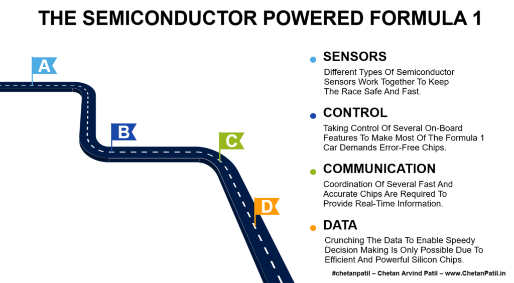
    Sensors: Silicon sensors play a vital role by capturing data around the car during the run time, which is a crucial part of the Formula One process. 

    Control: Formula One steering wheel consists o more than 30 buttons, all connected to a small handheld platform. Several tiny silicon chips ensure this communication is forwarded accurately to the car and the team.

    Different semiconductor chips enable fast and accurate decision-making. It is a crucial part of the race-winning strategy. Processing data and presenting it to the racing team is also a differentiating factor between winning and losing the race.

    Today, a Formula One car has more than 100 different types of simple to complex chips. Formula E (electric version of Formula One) has much more due to the electric power management system. It shows how semiconductor contributes to a Formula One championship.


    Picture By Chetan Arvind Patil

    Radio communication and data analysis is a big part of the Formula One championship. Both of them rely on silicon chips that can provide near-zero latency systems.

    Apart from utilizing existing solutions, semiconductor companies also have strategic partnerships (and sponsorship) with Formula One teams. It allows them to experiment with new solutions on a track and car that stresses the system to its limit.

    Communication: Real-time communication from the car, driver, and team allows faster decision-making. Doing so requires an error-free and near-zero latency silicon-driven system.

    Data: Crunching the data about how the car is moving, who is ahead and behind, how the engine performance is and whether the tires are in good shape is a big part of Formula One racing, and teams that make a quick decision using it eventually wins the race and the championship.

    Such a solution goes through several testing before the start of the championship and is eventually made into the final car if the testing results are promising. A centralized computer system to monitor car activity is one such example.

    The technology behind the Formula One car will keep evolving. It will also keep presenting opportunities for automotive companies to test ideas in an environment that can push the system to its limit. As the world moves towards a more chip-driven approach, Formula One itself presents as big technology and investment-driven platform to try out the best ideas.