Category: EDUCATION

  • The Semiconductor Learning Path – Build Your Own Roadmap Into the Industry

    Image Generated Using 4o


    Learning To Learn About The Semiconductor Industry

    The semiconductor industry is a maze of ideas, technologies, and challenges, an intersection of physics, chemistry, engineering, economics, and geopolitics.

    For an early engineer, it is easy to get lost in the details. Thus, how do you even begin to make sense of it all? What do you need to know? Where do you find the correct information? And how do you build fundamental skills that matter?

    It is not a field that can be mastered by simply reading a textbook. Learning about semiconductors is a process of learning how to learn, gathering knowledge from different domains, connecting dots across disciplines, and constantly adapting to new technologies and industry shifts.

    Let us explore how to build your roadmap into the semiconductor industry, enabling you to go beyond surface-level learning and develop real, practical expertise.


    Start With Curiosity And See The Big Picture

    Before diving into specifics like FinFETs or EUV lithography, step back and ask: What makes semiconductors so important? Why is the world investing over $1 trillion by 2030 into this industry? And what problems are semiconductors trying to solve today and in the future?

    As a beginner in this field, it is crucial first to understand the larger forces at play. What drives this industry? How do companies, countries, and technologies intersect? Why is there a global race to secure semiconductor supply chains? And how do these factors influence the way chips are designed, built, and tested?

    Let us break this down with a simple mental map:

    LayerFocus QuestionsExamples
    ApplicationsWhere are chips used?AI, automotive, smartphones, medical devices, etc
    Market ForcesWhat drives demand?AI workloads, EV growth, hyperscale data centers, consumer electronics, industrial automation
    Supply Chain & PolicyWho makes what, and where?Taiwan (TSMC: 55% of global foundry market), Korea (Samsung), US (Intel, Micron), Europe (ASML, Infineon), China (SMIC)
    Technical DomainsWhat are the core areas to learn?Design (EDA, architecture), fab (process tech, equipment), test (DFT, ATE), packaging (2.5D, 3D, chiplets)


    Where To Start Your Semiconductor Industry Learning and Exploration

    The semiconductor industry is not just a collection of devices and processes. It is a complex, global ecosystem driven by markets, applications, supply chains, and geopolitics. Understanding this broader context is crucial, as every technical decision, whether it involves a design feature, process node, or test method, ultimately ties back to it.

    That is why the first step in your learning journey is crucial. It should be to observe and map the landscape.

    This is about building awareness: Who are the key players? Where are the fabs? What are the dominant applications? How do global trends like AI, electric vehicles, and 6G impact chip demand? What bottlenecks and risks threaten the industry?

    It is essential to spend 1–2 months reading, watching, and listening, building a robust mental model of the industry before you dive into technical details. This preparation will give you the confidence to navigate the complexities of the semiconductor industry.

    Here is a table of recommended starting points to guide your exploration:

    ResourceWhat You’ll LearnLink
    SIA State of the Industry ReportsIndustry size, growth trends, global challengesSIA
    WSTS Market ForecastsRevenue by region, application, and nodeWSTS
    Deloitte & McKinsey Semiconductor OutlookMarket shifts, talent gaps, AI & EV demandDeloitte
    Tech Blogs (SemiWiki, EE Times, etc.)Real-world insights, design challenges, fab storiesSemiWiki
    Conference Keynotes (IEDM, DAC, SEMICON)Cutting-edge research, technology roadmapsIEDM, SEMICON

    Reading these sources is not about memorizing numbers or names, it is more about pattern recognition.

    For instance:

    • When you see that AI and automotive are driving new chip demand, you will understand why design teams are focusing on high-bandwidth memory and power efficiency.
    • When you read about foundry concentration in Taiwan and near-by region, you will grasp the geopolitical risks and supply chain vulnerabilities that shape investment decisions.
    • When you learn that testing and packaging costs can make or break profitability, you will appreciate why certain startups focus on advanced packaging solutions or automated test flows.

    This contextual knowledge will act as your anchor. It helps you ask better questions when you later study design, fabrication, or validation.

    For example: Why are specific nodes (e.g., 5nm, 3nm) so costly to manufacture? Why is there a shortage of skilled talent in fabs? Why are governments pouring billions into on-shoring chip production?

    The goal is not to become an expert in every domain yet, but to orient yourself in the industry’s landscape so that your future learning builds on a strong foundation.


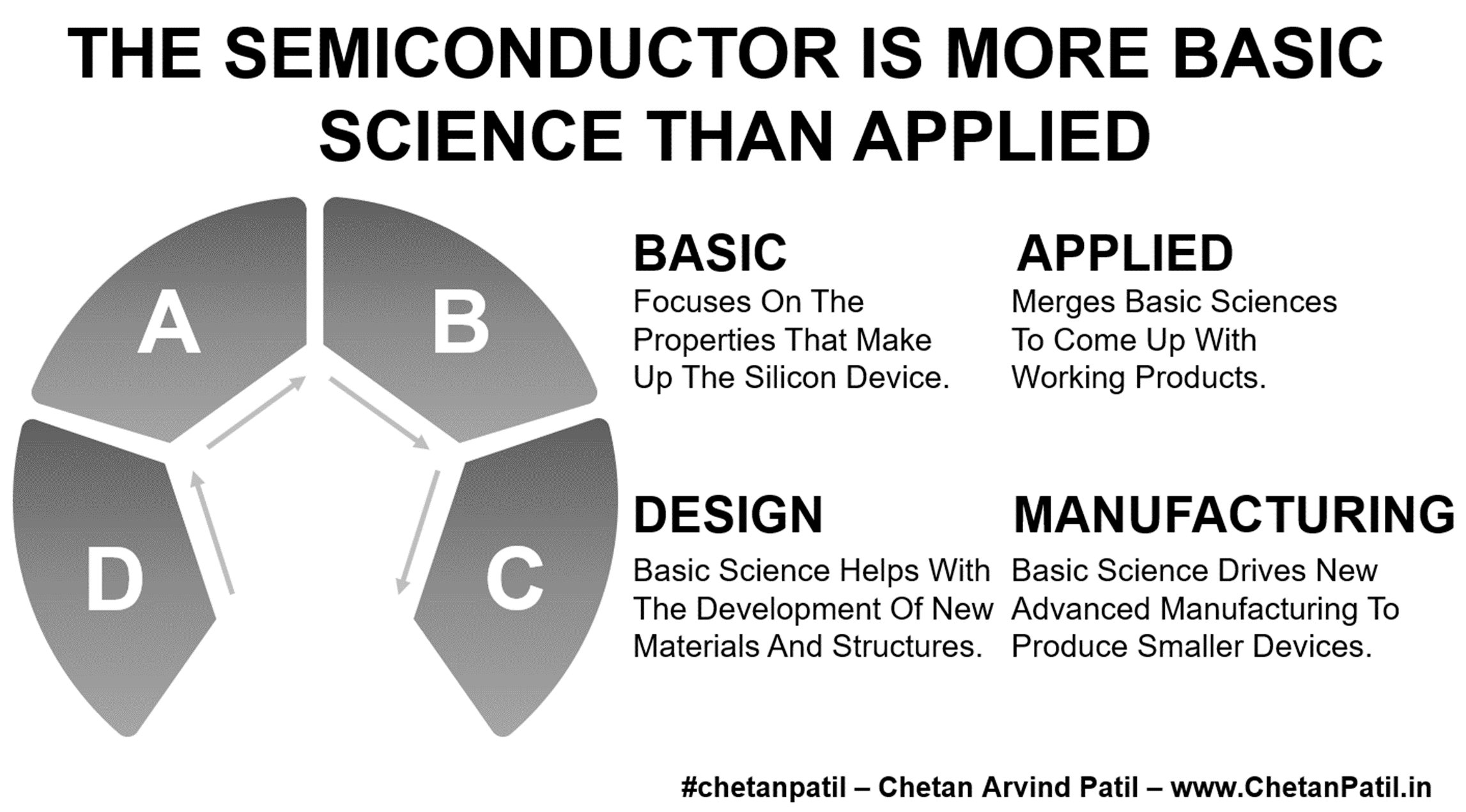
    Understand The Core Technical Domains And The Building Blocks

    Once you have a big-picture view of the semiconductor industry, its applications, markets, and supply chain, it is time to dive into the technical core: how chips are built.

    Semiconductors are not just one thing, they are a blend of physics, materials, design, fabrication, testing, and packaging. You do not need to know everything, but you should develop a working understanding of these key areas.

    Start with device physics. Learn how materials like silicon conduct electricity, how transistors switch, and how scaling pushes limits. This is where everything in a chip begins.

    Move to process and fabrication. This is about how chips are physically constructed using tools such as lithography, etching, and deposition. You will understand why advanced nodes, such as 5 nanometers, are so challenging and why yield is a critical factor in production.

    Learn design and architecture. This is where logic becomes circuits, and circuits become chips. Whether it is writing RTL, simulating circuits, or understanding a system architecture, this knowledge connects ideas to real hardware.

    Finally, explore testing, validation, and packaging. Testing ensures that a chip works across all conditions, and packaging serves as the bridge between the silicon and the real world. With 3D stacking and chiplets on the rise, the packaging is no longer an afterthought, it has become an integral part of the system design itself.


    Stay Current, Follow Trends, Reports, And Community Insights

    The semiconductor industry is in constant motion, technologies evolve, markets shift, and policies reshape priorities. Staying relevant means more than just learning the basics once, it is about cultivating the habit of continuous learning.

    Follow market reports, read industry insights, and engage with the community. Build a system for tracking trends and questioning how they connect to the technical foundations you are learning.

    This mindset sets great engineers apart. The best in the field are not just experts in one area, they are curious, connected, and adaptable. They understand how technical decisions relate to market demands, how design influences testing, and how global events can shape the future of chips.

    Here are a few suggestions to help you stay on track:

    • Subscribe to industry newsletters like SIA, Semiconductor Digest, EPDT, and WSTS. They will help you keep up with market data, reports, and policy updates
    • Attend webinars and technical talks; even one session a month from conferences like IEDM, DAC, or SEMICON can provide valuable insights
    • Follow semiconductor engineers and thought leaders on LinkedIn, people who share real-world problems, industry trends, and project breakdowns
    • Set a routine: Dedicate 30 minutes a day or 2 hours a week to learning and reflection
    • Start small projects: Simulate circuits, reverse-engineer a teardown, or write a summary of a technical paper
    • Share your learning: Write a LinkedIn post or blog, explain a concept to a friend, or discuss it with peers. Teaching reinforces learning

    As you build your roadmap in the semiconductor world, remember to stay curious, stay connected, and stay learning.

    That is the only way to keep up in this fast-moving industry and to grow into a professional who not only understands how chips work but why they matter.


  • The Semiconductor Manufacturing Training Through Virtualization

    Image Generated Using DALL-E


    Semiconductor And Virtualization

    In the ever-evolving landscape of semiconductor manufacturing, staying ahead of technological advancements and maintaining a highly skilled workforce is critical for success. While effective, traditional training methods often have significant costs, safety concerns, and accessibility limitations. Enter virtualization – a transformative approach that has revolutionized how the industry and academia train and educate individuals in the semiconductor industry.

    Virtualization leverages advanced technologies to create immersive, interactive, and highly realistic simulations of semiconductor manufacturing processes. Doing so offers many benefits that traditional methods cannot match.

    Application Of Virtualization In Semiconductor

    By leveraging advanced technology to create immersive and interactive environments, virtualization offers unparalleled learning and skill development opportunities. This innovative approach addresses many challenges associated with traditional training methods, providing a safer, more cost-effective, and flexible alternative.

    As the semiconductor industry advances rapidly, the need for up-to-date and comprehensive training programs becomes increasingly critical. Virtualization, with its inherent adaptability, meets this demand by enabling efficient, scalable, and highly effective training solutions.

    Below are some key applications of virtualization in semiconductor training, highlighting how it enhances the learning experience and prepares trainees for real-world scenarios:

    ApplicationDetails
    Process SimulationTrainees can experience and optimize various manufacturing processes in a risk-free virtual environment.
    Equipment Operation TrainingVirtual models of complex machinery help trainees learn how to operate and troubleshoot equipment effectively.
    Cleanroom ProtocolsSimulating cleanroom conditions allows trainees to practice maintaining contamination-free environments.
    Data Analysis And VisualizationVirtual tools teach trainees how to interpret and act on process data.
    Quality ControlVirtual environments replicate quality control scenarios, enabling trainees to identify defects and implement quality assurance measures.
    Design And Fabrication TechniquesVirtual platforms provide detailed simulations of design and fabrication techniques, enabling learners to understand and implement advanced methods.
    Supply Chain ManagementVirtual training includes modules on managing supply chains, understanding logistics, and optimizing the flow of materials in semiconductor manufacturing.
    Educational Courses And CertificationsVirtual platforms offer comprehensive courses and certification programs, ensuring learners are up-to-date with the latest industry standards.
    Collaborative ProjectsStudents and professionals can work together on virtual projects, simulating real-world collaboration and problem-solving scenarios.
    Virtual Reality ClassroomsImmersive virtual reality classrooms enhance the learning experience by providing interactive and engaging educational content.
    Remote Laboratory AccessVirtualization allows for remote access to laboratory experiments and equipment, enabling students to conduct experiments and gather data remotely.
    Interactive Tutorials And WorkshopsVirtual environments host interactive tutorials and workshops, allowing learners to gain practical skills through hands-on activities.
    Performance Tracking and AssessmentVirtual platforms track learner performance, provide detailed analytics, and offer personalized feedback to help improve skills and knowledge.

    As illustrated, virtualization’s applications in semiconductor training are diverse and impactful. From simulating complex manufacturing processes to facilitating remote learning and collaboration, virtualization empowers learners to acquire and refine critical skills in a controlled, realistic environment.

    This approach enhances the quality of education and ensures that the semiconductor workforce is well-prepared to meet the demands of a rapidly evolving industry. By embracing virtualization, semiconductor manufacturers can cultivate a highly-skilled, knowledgeable, and adaptable workforce ready to drive innovation and excellence.


    Picture By Chetan Arvind Patil

    Cost-Effectiveness And Scalability

    One of virtualization’s most compelling advantages is its cost-effectiveness. Establishing and maintaining physical training facilities with state-of-the-art equipment is a significant financial burden. Virtual labs, on the other hand, require minimal physical resources, reducing overhead costs substantially. Furthermore, these virtual environments are highly scalable, allowing for the simultaneous training of numerous individuals without additional infrastructure.

    Virtual environments are not just interactive, they are designed to provide trainees with a hands-on experience that is as close to real-world as possible. These environments can simulate everything from lithography and etching to cleanroom protocols and equipment operation. The immediate feedback provided in these virtual settings is a testament to the efficiency of the learning process, helping trainees understand and correct their mistakes promptly.

    Advantages Of Virtualization In Semiconductor

    The semiconductor industry is highly dynamic, with continuous technological advancements necessitating equally progressive training methods. Virtualization is a pivotal tool, offering significant advantages over traditional training approaches.

    Virtualization, with its realistic, interactive, and risk-free virtual environments, offers comprehensive and efficient training for semiconductor professionals. This modern approach addresses several critical challenges, ensuring trainees receive the highest quality education. Importantly, virtualization also minimizes costs and risks, providing a secure financial aspect to professionals’ training.

    Below are some of the key advantages of using virtualization in semiconductor training:

    AdvantageDetails
    Cost-EffectivenessResource Optimization: Virtual labs reduce the need for physical resources and equipment, which are often expensive and difficult to maintain.
    Scalability: Multiple students can access virtual environments simultaneously, allowing large-scale training programs without additional physical infrastructure.
    Safety And Risk ReductionEnhanced Safety: Virtual environments provide a secure learning space by eliminating the risks associated with handling hazardous materials or operating complex machinery. This safety feature instills confidence in trainees, allowing them to learn and experiment without fear.
    Error Tolerance: Mistakes made in virtual environments do not have real-world consequences, allowing trainees to learn from their errors without risk.
    Accessibility and FlexibilityRemote Learning: Virtualization enables remote training, allowing students and professionals worldwide to access the same high-quality educational resources.
    Flexible Schedules: Learners can access training modules conveniently, accommodating different time zones and personal schedules.
    Enhanced Learning ExperienceInteractive Simulations: Virtual labs can include interactive simulations that enhance understanding by providing hands-on experience with semiconductor manufacturing processes.
    Real-Time Feedback: Instant feedback in virtual environments helps learners understand their mistakes and correct them promptly.
    Up-To-Date TrainingRapid Updates: Virtual training programs can be quickly updated to reflect the latest advancements and technologies in semiconductor manufacturing.
    Customized Content: Training modules can be tailored to specific needs, ensuring learners have relevant and current knowledge.
    Collaboration And Skill DevelopmentCollaborative Platforms: Virtual environments can facilitate collaboration among students, researchers, and professionals, promoting the exchange of ideas and best practices.
    Skill Development: Virtual training emphasizes critical thinking, problem-solving, and technical skills essential for semiconductor manufacturing.

    As demonstrated, virtualization’s advantages in semiconductor training are extensive and transformative. By leveraging virtualization, the semiconductor industry can overcome many of the limitations associated with traditional training methods.

    This innovative approach enhances the learning experience and ensures that trainees are well-prepared for the challenges and opportunities of a rapidly evolving field.

    In the long term, embracing virtualization is essential for cultivating a skilled, knowledgeable, and adaptable workforce capable of driving the semiconductor industry forward.


  • The Future Of Semiconductor Education

    Image Generated Using DALL-E


    What Is Semiconductor Education

    The landscape of semiconductor education is pivotal to the continued innovation and growth in the tech industry, especially when designing and manufacturing digital and analog circuits, which play a critical role in various sectors, including computing, telecommunications, automotive, and consumer electronics.

    Semiconductor education is fundamentally about equipping students with the knowledge and skills to design, manufacture, and optimize semiconductor devices, which are the building blocks of all modern electronic circuits. This field merges principles from physics, chemistry, and electrical engineering to create components essential to electronic systems.

    Today’s semiconductor education is growing. It covers traditional topics such as silicon-based devices and circuit design. Still, it also keeps up with the times by integrating emerging subjects like silicon photonics, power semiconductors, and flexible electronic systems.

    However, keeping up with current trends is not enough. It is crucial to align the educational curriculum with the demands of future technology development. This proactive approach ensures that students are prepared for the future and can contribute effectively to the field of semiconductors.


    Challenges Facing Semiconductor Education

    Despite the advancements, semiconductor education faces several challenges that could hinder its progress. There is a notable disconnect between the skills taught in academic settings and the evolving needs of the industry, especially in specialized areas such as materials science, microfabrication, and quantum computing. The high cost of up-to-date equipment and materials makes it difficult for educational institutions to provide state-of-the-art learning experiences.

    Thus, it has become important for universities and colleges to come up with innovative ways in develop and keep semiconductor education aligned with industry requirements.

    ChallengeDescription
    Skills GapThere is a notable disconnect between the skills taught in academic settings and the evolving needs of the industry, particularly in specialized areas such as materials science, microfabrication, and quantum computing.
    High CostsThe expense of acquiring up-to-date equipment and materials makes it difficult for educational institutions to provide state-of-the-art learning experiences, limiting access to modern training and facilities.
    Scarcity Of Qualified InstructorsThere is a lack of educators with the most recent industry experience and advanced knowledge of the latest semiconductor technologies, challenging the delivery of current and relevant education.

    Picture By Chetan Arvind Patil

    Emerging Trends In Semiconductor Education

    The field of semiconductor education is witnessing significant transformations due to the integration of advanced educational technologies. Virtual laboratories and simulation software are becoming commonplace, enabling students to experiment with and design semiconductor circuits without costly physical lab setups.

    TrendDescription
    Online And Blended Learning FormatsAdopting hybrid education models combines online digital media with traditional methods, enhancing flexibility and global access.
    Hands-On Simulation ToolsIntegrating advanced simulation tools like CAD for VLSI design and SPICE enables virtual circuit design and testing, reducing the need for costly labs.
    Focus On Nanotechnology And Quantum ComputingIncreasing emphasis on cutting-edge fields such as nanotechnology and quantum computing to prepare students for advancements in fabrication and application.
    Industry-Academia CollaborationsPartnerships between universities and semiconductor companies to align curricula with industry standards, offering internships and access to professional tools.
    Specialized Degree ProgramsDevelopment of specialized degree and certification programs focused on semiconductor studies, from basics to advanced chip design, tailored to industry needs.
    Sustainability In Semiconductor ManufacturingThe incorporation of sustainability practices, including courses on low-power circuit design and recyclable materials, reflects the industry’s shift towards green manufacturing.

    Moreover, partnerships between academic institutions and industry giants are instrumental in bridging the gap between theoretical knowledge and practical skills. These collaborations help update curriculums with cutting-edge content and provide students with internship opportunities to gain hands-on experience.

    Educational policies and global initiatives further influence the structure and delivery of semiconductor programs, ensuring they meet international standards and industry demands.


    Looking Ahead: The Future of Semiconductor Education

    The future of semiconductor education is likely to be shaped by further integration of cutting-edge technologies like artificial intelligence (AI) and machine learning. These tools can revolutionize teaching methodologies and learning environments by enabling personalized learning paths and predictive analytics to improve student engagement and outcomes.

    As the semiconductor industry continues to evolve, educational institutions will need to anticipate future skills requirements and adapt their programs to prepare students for emerging roles in the design, fabrication, and testing of next-generation semiconductor devices.


  • The Semiconductor Is More Basic Science Than Applied

    Photo by Trnava University on Unsplash


    Semiconductor engineering is a field that distinguishes basic and applied science. On the one hand, it relies on a deep understanding of fundamental physics, such as the behavior of electrons in solids. On the other hand, it also requires the ability to apply this knowledge to the design and manufacture of practical devices.

    In recent years, semiconductor engineering has become increasingly reliant on basic science. It is because the challenges of miniaturizing and improving semiconductor devices are becoming increasingly complex. To address these challenges, semiconductor engineers must deeply understand the underlying physical principles.

    Examples of how chemistry, physics, and mathematics find use in semiconductor engineering:

    Chemistry: Chemists study the structure and properties of matter, including semiconductor materials. This knowledge drives the development of new semiconductor materials with improved properties, such as higher electron mobility or lower carrier concentration. For example, chemists have developed new methods for growing silicon crystals with fewer defects, which has led to the development of smaller and faster transistors.

    Physics: Physicists study the behavior of matter at the atomic and subatomic levels. This knowledge helps in understanding the behavior of electrons in semiconductor materials, which is essential for designing semiconductor devices. For example, physicists have developed models that describe how electrons move through semiconductor materials, which helps create transistors that operate at high frequencies.

    Mathematics: Mathematicians use their knowledge of numbers and logic to solve problems in various fields, including semiconductor engineering. For example, mathematicians use statistics to analyze the performance of semiconductor devices, and they use calculus to design semiconductor circuits.

    In addition to design, basic science plays an increasingly important role in semiconductor manufacturing. For example, developing new lithography techniques requires a deep understanding of the physics of light and matter.


    Picture By Chetan Arvind Patil

    The field of semiconductor engineering is rapidly evolving, and the demand for semiconductor engineers with a strong foundation in basic science will grow in the coming years. It is crucial to ensure the basic science behind the design and manufacturing of semiconductors progresses forward.

    Design: In design, basic science enables the development of new transistor materials and structures. For example, researchers are using carbon nanotubes and graphene to create smaller and faster transistors than traditional silicon transistors.

    Manufacturing: Basic science drives new lithography techniques in manufacturing that produce smaller and more precise features. For example, researchers use extreme ultraviolet (EUV) lithography to create parts that are just a few nanometers.

    As the challenges of miniaturizing and improving semiconductor devices become more complex, semiconductor engineers will need to understand the underlying physical principles deeply. It will require close collaboration between semiconductor engineers, physicists, chemists, and materials scientists, thus opening up opportunities for science undergraduate and graduate students.


  • The Future of Education And Learning

    The Future of Education And Learning

    Photo by Changbok Ko on Unsplash

    Education is the key to learning various aspects of life and different career options. It enables the development of skills. There have been different way to learn in order to enable individuals with wider thoughts and options from career point of view.

    Many prefer the traditional way of education by enrolling in schools/universities to acquire certificate/degree/diploma after fulfilling required criteria. On other hand few also prefer to learn everything on their own from different sources whether it is library, internet or attending different events, workshops and conferences. This may not lead to a formal certificate/degree/diploma, but the goal for such learners is not credentials.

    Whichever path one takes, it always leads to same goal: Education and Learning.

    In the last decade, there has been lot of changes in the form of delivery of education and different modes of learning. Majority of the changes have been due to the advancement of technology that has allowed the content to be delivered easily, mainly thanks to the innovation due to internet and connectivity.

    With such abundance of sources readily available at the click of the button, the mode of learning is going to change from Traditional Education to Always Be Educating And Learning From Anywhere.

    Lets take a look at different forms of sharing knowledge and educating people, and also how it has evolved by building on top of previous mode of education delivery.

    PRE-INTERNET TRADITIONAL LEARNING

    What And How:

    • This is the 101 form of education where schools and universities were established. Students will enroll and follow a set curriculum before earning the certificate/degree/diploma. This still exists, but slowly it is adapting and finding ways to make it more convenient rather than moving to a location to acquire knowledge.
    • One of the key benefits of traditional learning is the massive one-to-one interaction students have on daily basis. This not only allows growth from education and knowledge point of view, but also help students develop. networking and interpersonal skills. On top, individuals can engage in extra curriculum activities that can help them physically, socially and mentally.
    • Another key driver of traditional learning is research and development (R&D). R&D is key to future developments. Even internet which you are using today to read this blog was a R&D project. And, today it is the backbone of everything in the world.
    • There has been growing concerns and questions on the need to have traditional learning, however it is key to many future advancement along with innovation leading to better quality of life.
    Photo By Chetan Arvind Patil

    Problem Solved:

    • Interaction with peers
    • Learning future options
    • Extra curriculum development
    • Access to the formal education

    Problem Created:

    • Become more routine task
    • Difficult to find the best teachers
    • Started getting expensive to afford
    • Not all schools/universities have the same facilities, resources, financials and quality

    PRE-INTERNET TRADITIONAL LEARNING VIA DISTANCE LEARNING

    What And How:

    • One of the major drawbacks with traditional learning is that one has to be physically present in the place where the schools/universities are located. This started becoming a problem for those whose town/cities were lacking educational institutes.
    • Another gap that traditional learning created was that the quality of education started varying from place to place. Few will have the best of facilities and teachers, and rest will always try to balance thus leading to imbalance. This started depriving students the opportunity to learn from the best if they cannot afford to enroll/move.
    • Eventually, all these problems lead to the invention of distance learning. Which allowed students to enroll in the best schools and universities without having to be physically present.
    • The content and material related to the classes is provided as per the schedule via snail mail. Then at the end of the season students can take exams at local centers. The outcome the decides whether they get to hold the certificate/degree/diploma from the coveted schools and universities.
    • Distance access to best schools and universities lead to increase in literacy and opened employment opportunity
    Photo By Chetan Arvind Patil

    Problem Solved:

    • Adaptive scheduling and enrollment
    • Low cost compared to traditional learning
    • Made individuals eligible for higher education
    • Access to formal education from the best schools and teachers over correspondence

    Problem Created:

    • Lack of in person interaction with teachers and peers
    • With growing option it became difficult to choose the best
    • Even industry started to question whether distance learning is legit
    • Practical learning was not part of correspondence due to lack of physical access to the labs

    POST-INTERNET HYBRID TRADITIONAL LEARNING

    What And How:

    • Post internet many things changed and allowed learning being more a mix of traditional and online, also knows has hybrid traditional learning.
    • Distance correspondence courses were now offered online in real time. Schools and teachers were now equipped with more knowledge and advanced technological tools.
    • Most of the students who can afford will enroll in person and those who cannot started opting for online mode of learning. Both ways allowing access to same education.
    • Curriculum of the courses that required labs were adapted for online students.
    • Course material distribution started happening via online websites and software rather than physical distribution of assignments as hard copy.
    Photo By Chetan Arvind Patil

    Problem Solved:

    • Access to the courses in real time
    • Option to enroll in online mode of learning
    • Materials can be accessed anytime anywhere
    • Made education more exciting and little bit affordable based option to enroll courses online rather than in person

    Problem Created:

    • Education became fast paced rather than learning based
    • Not all courses were taught online, thus the options were limited
    • Not all major were able to make most of it like medical education where one needs to be with patients as the course moves forward
    • Everyone’s learning was depended on the mode of education opted. Those with in person option had better access to teachers than those using online mode

    POST-INTERNET HYBRID TRADITIONAL LEARNING WITH OVER THE TOP CONTENT

    What And How

    • Over The Top (OTT) is a way of providing services on top of existing services. For example, a cellular company providing educational apps on top of the voice service it provides. A startup with extra curriculum to create existing course more interactive is another example of OTT.
    • OTT in education applies to both teachers and students. As it is designed to make both the traditional and hybrid approach better
    • There are third party companies that tie up with schools and universities to ensure that learning is more interactive, practical and is built on top of years of research carried out across the world.
    • OTT is not just about learning to seek certificate/degree/diploma, it has different modes too:
    Photo By Chetan Arvind Patil

    Problem Solved

    • Made education more fun
    • Improved quality of courses
    • Increased real time interaction of students and teachers
    • Practicals become more knowledgeable based based on real life examples

    Problem Created

    • Not all schools and students could afford the OTT services
    • Additional cost and time to learn courses other than traditional curriculum
    • Not available to villages and towns which are still lacking resources and finance
    • It made education more expensive as the OTT fee was passed on to the students

    FUTURE OF EDUCATION AND LEARNING

    COVID-19 drove closure of schools and universities around the globe. This forced cancellation of academic session in many countries. Places where schools/universities that had the infrastructure were able to switch to online mode and complete the curriculum. This also drove demand of online mode of learning. Also pushed workshop and conferences to make use of webinars to deliver the per-scheduled content.

    In future, learning instead of being just about attending classes will move to always be educating and learning from anywhere. It will not matter where the content is coming from, education seeker will keep learning from different resources as per their need and requirement. They will also continue to seek traditional credentialing process to widen their reach and networking.

    Photo By Chetan Arvind Patil
    Photo By Chetan Arvind Patil

    Future of education and learning is everywhere:

    • Traditional learning will be the foundation
    • Mixed reality will enable virtual laboratories
    • Peer mentoring will be vital part of curriculum
    • Hybrid approach with option to attend classes online and/or offline
    • Distance learning in form of special issues and books for remotest areas

    Whether or not formal credentialing in form of certificate/degree/diploma will still exists is left for expert to talk about. However, adapting and learning from different sources is going to be very vital and key skill of next generation. This will also mean countries across the globe will have to have reliable and affordable digital infrastructure.

    Always Be Educating And Learning From Anywhere


    PSA

    Steve Blank‘s talk on The Secret History of Silicon Valley shows the importance of how traditional education driven by research and development enabled the foundation of Silicon Valley.