The rapid progress of semiconductor technology is built on a simple principle: by scaling transistors down, more components can be packed into a chip, resulting in higher performance.
Over the past half‑century, this strategy has delivered exponential growth in computing power, but it has also unleashed a hidden cost.
As manufacturing processes have become more complex and factories have grown larger, the energy required to produce each wafer and to operate cutting-edge tools has risen significantly.
Let us examine how the pursuit of smaller features and increased functionality influences the energy footprint of semiconductor manufacturing.
Scaling’s Hidden Energy Burden
The paradox of semiconductor scaling is that even as transistors have become more energy-efficient, the total energy required to manufacture chips has continued to rise. In the early 1980s, a survey by SEMATECH and the U.S. Department of Commerce reported that producing a square centimetre of wafer consumed about 3.1 kWh of electricity.
By the mid-1990s, studies published in Elsevier research on fab energy efficiency showed that improvements in equipment and clean-room design reduced this to roughly 1.4 kWh/cm².
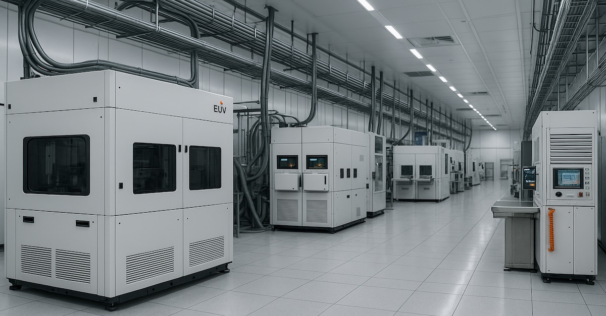
However, this trend reversed in the era of advanced nodes. A recent life-cycle assessment by imec’s Sustainable Semiconductor Technologies program found that cutting-edge processes, such as the A14 node, require multiple patterning and extreme-ultraviolet (EUV) lithography, resulting in energy intensity exceeding 4 kWh/cm². EUV scanners themselves, according to open data on EUV lithography, consume more than 1 megawatt each and use nearly 10 kWh of electricity per wafer pass, over twenty times more than their deep-ultraviolet predecessors.
On the other hand, global energy consumption figures underscore this burden. Azonano’s 2025 industry analysis reported that fabs consumed around 149 billion kWh in 2021, with projections reaching 237 TWh by 2030, levels comparable to the annual electricity demand of a mid-sized nation. The impact of AI is even more dramatic: TechXplore’s reporting noted that AI chip production used 984 GWh in 2024, a 350% increase from the previous year, and could surpass 37,000 GWh by 2030. Meanwhile, SEMI industry reports warn that a single megafab now consumes as much electricity as 50,000 households, while Datacenter Dynamics highlights that TSMC alone accounts for nearly 8% of Taiwan’s electricity use.
In short, scaling has delivered smaller transistors but at the cost of turning modern fabs into some of the largest single consumers of electricity on the planet.
Why Fabs And Tools Consume So Much Power
Building chips at the nanoscale demands extraordinary precision, and that precision comes with enormous energy costs. Modern fabs resemble self-contained cities, running fleets of machines that deposit, etch, inspect, and clean microscopic features while maintaining particle-free environments.
Lithography tools stand out as the biggest energy hogs, but facility systems and even raw material preparation also contribute significantly. The table below highlights how different elements of semiconductor manufacturing stack up in terms of power use and impact.
Taken together, lithography, process equipment, facility systems, and upstream materials explain why fabs are among the most power-intensive industrial facilities in existence.
Each new technology node multiplies the number of steps and tools, pushing power use higher even as individual machines become more efficient.
The race to build faster and more capable chips has delivered extraordinary benefits, but it has also exposed the mounting environmental costs of progress. Moore’s law may evolve, but the laws of thermodynamics remain fixed: every advance demands energy.
In all, the path forward lies in pairing innovation with responsibility, thus prioritizing energy-efficient design, renewable power, and sustainable manufacturing. The choices made today will determine whether future chips are not just smaller and faster, but also cleaner, greener, and more responsible.
The Dual Imperative Of Innovation And Sustainability In Semiconductor Manufacturing
Semiconductors are the backbone of countless technologies, from smartphones and computers to medical devices and renewable energy systems. As the demand for more powerful and efficient devices grows, the semiconductor industry faces the dual imperative of driving innovation while committing to sustainability. Thus, the energy-intensive nature of semiconductor manufacturing presents a significant challenge but also underscores the industry’s crucial role in shaping a sustainable future.
According to the International Energy Agency (IEA) report, semiconductor fabrication plants can consume as much electricity as cities. For instance, a single large fab can use up to 100 megawatts of power per hour, equivalent to the electricity consumption of 80,000 U.S. homes.
Another Semiconductor Industry Association (SIA) study revealed that the global semiconductor industry consumed about 100 terawatt-hours (TWh) of electricity in 2020, accounting for nearly 0.3% of the world’s total electricity use. This level of consumption not only has significant cost implications but contributes to the industry’s carbon footprint.
This high energy usage underscores the urgent need for the industry to find a balance between advancing technology and minimizing environmental impact, a task of paramount importance.
The Energy Footprint Of Semiconductor Manufacturing
The energy footprint of semiconductor manufacturing is substantial, with significant consumption at every stage of the production process. Each step requires large amounts of energy, from the initial wafer production to photolithography, etching, and testing.
Source: Several Technical Reports And Research Papers
Furthermore, the production and use of AI chips, which demand intensive computational power for training machine learning models, significantly escalate energy requirements. To put this into perspective, training a single AI model, such as GPT-3, can consume the energy equivalent of driving a car for over 700,000 kilometers.
Challenges In Balancing Innovation And Sustainability
Balancing innovation and sustainability in semiconductor manufacturing presents a multifaceted set of challenges. However, these challenges also present opportunities for innovation. As chip designs advance, particularly with the push towards smaller nodes like 5nm and beyond, the complexity of manufacturing processes increases exponentially. It demands more sophisticated and energy-intensive equipment and exacerbates production’s environmental and resource impacts. For instance, cutting-edge technologies such as Extreme Ultraviolet (EUV) lithography, essential for creating these advanced chips, consume significantly more power than older methods, making energy efficiency a critical concern.
The table below details the key challenges, their descriptions, and the technical statistics associated with balancing innovation and sustainability in semiconductor manufacturing:
Challenge
Description
Technical Stats And Key Points
Advanced Node Technologies
Increased complexity and energy demands with smaller node technologies.
– EUV lithography consumes up to 2.5 MW per system. – Smaller nodes (5nm and below) require advanced, energy-intensive processes. – Lower yields increase energy and resource consumption.
Short Product Life Cycles
Rapid innovation leads to frequent upgrading and increased electronic waste.
– Over 50 million metric tons of e-waste generated annually. – Projected to reach 74 million metric tons by 2030. – Obsolete semiconductor devices contribute significantly to e-waste.
Environmental and Resource Impacts
High greenhouse gas emissions, significant water usage, and chemical management challenges.
– Semiconductor industry’s emissions projected to increase by 24% by 2030. – A single fab can use up to 10 million gallons of water per day. – Use of hazardous chemicals in manufacturing processes.
Economic Considerations
High costs of sustainable practices and competitive pressures to reduce costs.
– Significant upfront investments in energy-efficient technologies and renewable energy sources. – Balancing short-term competitiveness with long-term sustainability goals.
AI Chip Manufacturing
High energy demands for training and inference tasks in AI applications.
– Training a large AI model like GPT-3 can consume up to 1 MW of power continuously over several weeks. – AI inference tasks in data centers require 10-20 kW per rack.
Furthermore, the industry’s rapid pace of innovation leads to shorter product life cycles, contributing to the growing problem of electronic waste. Older models quickly become obsolete as new, more powerful chips develop, leading to increased disposal rates and significant environmental impacts. The industry’s reliance on large quantities of water, hazardous chemicals, and energy complicates efforts to achieve sustainability, especially as semiconductor fabs continue to scale up to meet global demand.
Economic factors also play a crucial role in this balancing act. Implementing sustainable practices often involves substantial upfront costs, which can be challenging for companies striving to maintain competitiveness in a fast-paced market. Additionally, the high energy demands associated with the production and use of AI chips add another layer of complexity to sustainability efforts. Training large AI models requires immense computational power, increasing the energy footprint of data centers housing these chips.
Sustainable FutureIs Key
Intel and TSMC are leading significant changes in the semiconductor industry’s approach to sustainability, focusing on advancing energy efficiency in their manufacturing processes. Both companies have made substantial investments in research and development, setting industry standards. TSMC, for example, has committed to transitioning entirely to renewable energy by 2050, with 25% of this target already met by 2020. On the other hand, Intel is developing advanced cooling systems and refining manufacturing techniques to reduce energy consumption and environmental impact.
The semiconductor industry’s focus on sustainability extends globally, as seen in efforts to integrate renewable energy into operations. Samsung, for instance, is implementing renewable energy solutions across its semiconductor plants, including regions such as the U.S., China, and Europe. The industry’s shift towards on-site renewable energy installations, such as solar panels and wind turbines, aims to reduce reliance on fossil fuels and lower carbon emissions on a global scale.
Government support and industry collaboration are crucial to sustaining these efforts. The U.S. Department of Energy’s Semiconductor Manufacturing Initiative is vital in advancing these goals through funding and incentives for energy-efficient innovations. Similarly, global initiatives like the World Semiconductor Council’s Environmental Safety and Health Task Force foster international cooperation on sustainability practices. Additionally, adopting circular economy principles, such as IBM’s recycling of silicon wafers for the solar industry and the reuse of materials from older chips, is helping to create a more sustainable future for the industry.
Take Away
The semiconductor industry stands at a critical juncture where the need to innovate must be balanced with the imperative of sustainability. The sector can significantly reduce its environmental impact by adopting energy-efficient technologies, integrating renewable energy sources, and embracing circular economy principles.
As we look to the future, sustainable practices will be essential for continued growth and success in semiconductor manufacturing. The path forward requires a concerted effort from industry stakeholders, governments, and consumers to prioritize sustainability in semiconductor production.