Category: FAB

  • The Semiconductor FAB AI

    Image Generated Using DALL-E


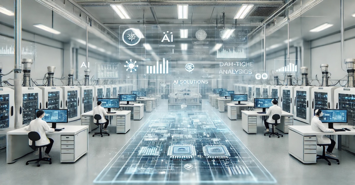
    Integration Of AI In FAB

    The semiconductor industry has long been constantly pushing the boundaries of what technology can achieve. As it nears the physical limits of what is possible, the next transformative leap is not surprising but inevitable: Artificial Intelligence (AI).

    Semiconductor manufacturing is inherently a data-driven process. Modern fabs generate massive amounts of data at every production stage, from individual tools to workflows. Yet, much of this data remains untapped, leaving valuable insights on the table. AI is poised to change that, unlocking the potential of this data for more intelligent, real-time decision-making.

    By embedding AI algorithms into manufacturing workflows, fabs can unlock unprecedented capabilities that drive efficiency, precision, and innovation:

    • Real-Time Process Optimization: By analyzing vast amounts of data in real-time, AI ensures that manufacturing processes stay within optimal ranges, reducing waste, improving efficiency, and maintaining consistent product quality.
    • Defect Prediction and Variability Reduction: AI minimizes variability and enhances process consistency by identifying anomalies that might otherwise go unnoticed. The result is a significant improvement in overall yield, fewer defective chips, and a more reliable manufacturing pipeline capable of meeting the industry’s growing demands.

    AI’s capacity to detect minute changes that might elude human operators, such as a slight drift in chemical concentrations, offers a game-changing advantage. These systems can respond instantaneously, making precise adjustments that prevent quality issues and reduce inefficiencies. This results in fabs that operate with greater precision, reliability, and output quality, paving the way for the next generation of semiconductor manufacturing.

    Examples Of AI In Semiconductor FABs

    Below are some of the most impactful examples of how AI is reshaping semiconductor fabs.

    Application AreaAI RoleImpact
    Computational LithographyOptimizes mask designs and exposure settings for better resolution.Improved pattern accuracy, reduced distortion, and higher yield.
    Fault Detection and Classification (FDC)Analyzes real-time equipment data to detect and classify faults.Faster fault resolution, reduced defects, and minimized downtime.
    Predictive MaintenancePredicts equipment failures before they occur.Avoids unplanned downtime, extends equipment life, and saves costs.
    Metrology and Process ControlIdentifies process drifts and predicts deviations.Enhanced process control, fewer defects, and improved yield.
    Wafer Map Pattern AnalysisDetects defect patterns and correlates them to fab conditions.Faster root cause analysis and reduced recurring defects.
    Design-Technology Co-Optimization (DTCO)Simulates impacts of manufacturing on design and suggests adjustments.Reduced development costs, optimized designs, and faster time-to-market.
    Supply Chain OptimizationAnalyzes supply chain data to forecast demand and identify risks.Improved resilience, reduced delays, and optimized inventory management.
    Virtual MetrologyPredicts metrology outcomes based on process data.Faster validation, reduced sampling needs, and lower costs.
    Automated Recipe GenerationGenerates optimal process recipes through simulations.Faster ramp-up of tools and processes, fewer trial-and-error iterations.
    Advanced Process Control (APC)Predicts process drifts and implements real-time corrections.Reduced variability, higher yield, and more stable processes.

    Talent And Skills Required For AI Integration In Semiconductor FABs

    Integrating AI into semiconductor fabs requires a unique mix of technical, analytical, and industry-specific skills. As fabs generate terabytes of data daily, expertise in data science, machine learning, and big data platforms is essential to transform raw data into actionable insights that improve processes and yield.

    Equally important is a deep understanding of semiconductor manufacturing processes like lithography, etching, and metrology. Engineers with hands-on experience ensure AI models are practical and accurate, while advanced AI expertise in neural networks and frameworks like TensorFlow enables real-time optimization and predictive maintenance.

    Leadership and project management also play a critical role, aligning multidisciplinary teams and ensuring smooth execution. Finally, innovation and problem-solving are indispensable for tackling the unique challenges of this evolving industry.

    Cost Implications Of AI Integration In Semiconductor FABs

    AI integration in semiconductor fabs requires significant investments in infrastructure, including high-performance computing, cloud or edge solutions for seamless data collection and AI model integration. These upfront costs can reach millions, depending on the scale and requirements.

    Despite the high initial expense, the long-term ROI often justifies the investment. AI enhances yield by reducing defects, optimizing processes, and increasing revenue. Predictive maintenance prevents costly downtime, while AI-driven efficiencies cut waste, energy consumption, and material costs, making operations more sustainable and cost-effective.

    While costly, AI integration is a strategic investment that provides fabs with a competitive edge. By improving yield, minimizing downtime, and streamlining processes, semiconductor manufacturers can achieve sustainable, long-term profitability.


  • The Semiconductor FAB Construction State

    Image Generated Using DALL-E


    Image Credit: McKinsey & Company


    Image Credit: SIA


  • The New Semiconductor FAB Impact

    The New Semiconductor FAB Impact

    Photo by Anne Nygård on Unsplash


    In the coming few years, several new semiconductor FABs will start production. Several of these were part of long-term semiconductor requirements. Few started construction based on the semiconductor shortages and the push to mitigate such a scenario in the future. These new FAB required years of planning and have invested billions of dollars. Thus, the impact of these semiconductor FABs on the semiconductor industry is going to be significant.

    One of the impacts is the generation of employment, which will bring a new workforce to the semiconductor industry. It will also benefit the economy in the long term. And, for FABs situated closer to universities, such development can also drive industry-academia collaboration, which has the potential to keep supplying skilled resources.

    Employment: New Employment Generation Opens New Career Opportunity.

    Options: There Are Several Options For The Semiconductor Companies To Select From.

    Apart from employment, the new semiconductor FABs will provide more options to the semiconductor industry. These options will ensure the FAB-LESS companies have more FABs to reach out to and thus can also enables a way to diversify the manufacturing of their products.

    New semiconductor fabrication capacity also restores the supply and demand balance. Thus, reducing the overall cycle time. However, doing so demands time and continuous investment, and it is not always an easy process.


    Picture By Chetan Arvind Patil

    The positive impact of new semiconductor FABs is many and not limited to employment and options. However, there are also downsides to having more semiconductor FABs.

    One such downside is the oversupply or overcapacity. While new FABs are certainly going to provide more options to the industry. However, market demand also plays a key role. If the market demand is strong, the new FABs will be 100% occupied. If not, then there is a strong possibility that the new FABs might not be able to run at 100% throughput to drive the envisioned break-even point.

    Supply: Over Capacity Can Negatively Impact The Semiconductor Manufacturing Ecosystem.

    ROI: Market Demand Can Impact The Return On Investment.

    Negative market demand while the new FABs are coming up is not the best scenario. It raises questions about the ROI and also puts the investment at risk. While the FABs have already done the groundwork to mitigate such a situation. In many cases, it is not possible to eliminate such risks.

    The benefits of the new semiconductor FAB are positive only as it not only drives more capacity but also brings a new type of semiconductor technology that can benefit the semiconductor industry for the decades to come.


  • The Growing Need To Adopt Multi-Technology Semiconductor Fabrication

    The Growing Need To Adopt Multi-Technology Semiconductor Fabrication

    Photo by Henry & Co. on Unsplash


    The semiconductor fabrication process is complex and costly, and it takes a lot of time to fabricate advanced solutions. Apart from the technical and business hurdles, the ability to develop one specific type of semiconductor device node is not resource-friendly. It also drives the demand to continuously invest in new facilities, which may or may not be ROI friendly.

    Multi-Technology Semiconductor Fabrication: Either Two Existing In-Demand Technology Can Be Fabricated At The Same Facility Or At Least Allow The Ability To Quickly Re-Spin The Existing Facility To A New One.

    This problem is getting more expensive with the launch of advanced technology nodes that require a new type of process flow, material, and equipment, which in turn requires a dedicated new facility. It is also evident from the number of fabrication facilities that are coming up and are focused on technology that will drive the semiconductor industry towards the angstrom phase.

    Long: With Every New Semiconductor Process Technology, The Fabrication Process Is Becoming Longer.

    Multi: Fabrication Facility Should Provide Multi-Technology Node Option Or Have The Ability To Expand Easily.

    The big question is whether there is a process to minimize the impact of the new advanced node on the need for dedicated and new facilities? The short answer might be no, but strategically it should be possible to develop a new facility with a focus on the ability to enable multi-technology processes today or tomorrow.

    It certainly does not mean that the overall cost will be lower when the time comes to enable optional technology. However, if planned well, solutions to parallelize the fabrication of multi-technology in the same facility today or at least how to minimize the future upgrades (apart from spinning off a new facility) to lower the overall expenditure should be feasible.


    Picture By Chetan Arvind Patil

    In many cases, the ability to focus on current and future technology nodes are not feasible due to the different support system required to enable future technology. At the same time, the fabrication cost of existing technology is increasing. This cost will go up further for the next-gen technology. Thus, re-planning and re-investing (following Moore’s law) becomes a lengthy process that is not always technology and business-friendly.

    Incorporating multi-technology where either two existing in-demand technology can be fabricated at the same facility or at least allow the ability to quickly re-spin the existing facility to a new one is the need of the hour. Today, there are clusters of fabrication facilities nearby that cater to different technology nodes. However, each of these demands dedicated resources that double the amount of investment.

    Cost: Moving From Single To Multi Will Allow Greater Control Over Fabrication Cost.

    Time: Time To Bring New Technology In A Multi-Technology Fabrication Can Become Shorter.

    The number of semiconductor manufacturing companies focusing on advanced nodes is limited. If the cost to bring in future technology grows further, it will reduce the number of semiconductor manufacturers focused on advanced nodes. Overall, it will make the semiconductor supply chain very fragile, and solutions to mitigate such situations are needed.

    Multi-technology can be a way to adopt multiple technologies today and build a facility for both together. It can also be an avenue to make future technology nodes more resource friendly. It will also demand additional work and capital. However, preparing for two technology or running two in parallel (in collaboration with equipment, material, and other technology providers) can certainly open up an option to lower the future semiconductor manufacturing cost.


  • The Impact Of Lithography On Semiconductor FAB

    The Impact Of Lithography On Semiconductor FAB

    Photo by Laura Ockel on Unsplash


    More than 50% of the semiconductor FAB (fabrication) cost is due to equipment and tools. Any given FAB has hundred different types of these, and without the required tools and equipment, the FAB cannot work efficiently. One piece of equipment that drives the semiconductor fabrication process forward is lithography.

    There are several aspects of semiconductor fabrication that has driven by lithography equipment. Yield and defect are two such examples from the technical point of view. It is the primary reason why semiconductor fabrication focuses a lot on which type of lithography technology to deploy. Eventually, products with low yields and high defect rates will not be market-qualified.

    Yield: Lithography equipment plays a vital part in achieving the required target process yield.

    Defect: Defect free masking is an important part of semiconductor fabrication made possible by lithography.

    Yield and defect are also dependent on the complexity of the semiconductor product. However, lithography equipment is supposed to handle the complex process. With semiconductor manufacturers focusing on next-gen advanced technology nodes, the importance of error-free lithography equipment will increase further.

    Semiconductor process technology is dependent on lithography and plays a crucial part in deciding how the FAB throughput will be. It is why semiconductor manufacturers worldwide are focused on acquiring the latest lithography equipment to upgrade existing FABs or build a new ones.


    Picture By Chetan Arvind Patil

    From a technical point of view, lithography equipment plays a vital role, and apart from yield and defect, there are more process-related criteria that lithography fulfills. However, from the business side too, the lithography equipment plays an important part.

    Two ways in which lithography equipment helps from a business point of view are capacity and break-even point. When it comes to building or upgrading FABs, lithography decisions are crucial. The reason being the solutions that the semiconductor FAB wants to make should be proven with different process steps, including the one executed by the lithography. In many cases, lithography often becomes the bottleneck due to the complex process.

    Capacity: FAB expansion and upgrade are directly related to the lithography equipment performance.

    Break-Even: Lithography also plays a critical role in achieving the FAB Break-Even Point.

    Semiconductor FAB capacity is directly associated with lithography due to the process node. The majority of the semiconductor FABs are opting for a new process node, and the decision on which type of xUV technology to use becomes an important parameter. Lithography also allows FABs to achieve faster break-even by continuously processing large numbers of defect-free and good-yielding wafers.

    Semiconductor capacity building is speeding up, and with technical/business impacts, lithography will play a big part. There are several concerns about lithography equipment shortage, and the path to successfully operating the new FAB will not be easy. Semiconductor manufacturers will have to focus on mitigating the lithography equipment shortage so that the investment done has a long-lasting impact.


  • The Growing Focus On Semiconductor Fabrication

    The Growing Focus On Semiconductor Fabrication

    Photo by Vishnu Mohanan on Unsplash


    Since the semiconductor shortage started, private semiconductor players and public bodies have focused on semiconductor manufacturing. The primary reason impact semiconductor shortage had on all other industries that heavily rely on semiconductor solutions.

    One of the positive impacts of semiconductor shortage (which ideally should be called a semiconductor opportunity) is the conversation around how to mitigate such shortage scenarios in the future. The best approach is increasing the semiconductor manufacturing capacity, but it also comes with several resources and investment constraints.

    Private: Focusing on market-driven technology requirements and upgrading/building semiconductor fabrication capacity.

    Public: Focused on creating an ecosystem for private players to either expand existing in-country semiconductor fabrication networks or create a new one from scratch.

    It is more valid for semiconductor fabrication. It takes two to three years to build any new facility. After that few more years to break even. All while semiconductor technologies keep changing and the cost increases year on year. On another side, post-fabrication semiconductor manufacturing (OSAT to ATMP) is still (compared to semiconductor fabrication) on the lower (but not easy to build) side when it comes to cost and resource planning.

    To mitigate any possible future semiconductor shortages, the private players and public bodies are taking different approaches, with the solve goal of mitigating future potential semiconductor shortages. Whichever path private and public players opt, the end impact is positive only. More so, when everything in day-to-day life is getting semiconductor driven.

    Semiconductor capacity building leads to several types of positive impacts. Removing dependency and catering to in-country demand are a couple of such examples.

    Dependency: Building semiconductor fabrication capacity allows countries to become more independent. In the long run, it also encourages homegrown products for in-country demand.

    Demand: A cluster of semiconductor fabrication has the potential to bring balance to any future supply and demand cycle.

    Dependency is all about ensuring the private players and governments are focused on creating semiconductor goods that make them independent in the long run. It is a vital process as several national critical infrastructures today require semiconductors. Thus fabricating these products in-house/in-country has is more important than ever.

    Building the semiconductor fabrication capacity also restores supply and demand balance. Thus, reducing the overall cycle time. However, doing so demands time and continuous investment.


    Picture By Chetan Arvind Patil

    Apart from dependency and demand, the two other factors that push private players and public bodies to focus on semiconductor fabrication are leadership and advancement.

    Leadership is about competition within the industry and also among the different governments. The hyper-connected and technology-enabled world has changed the definition of the superpower. It is why the governments are competing with each other and are coming up with industry-friendly policies.

    Today, this solution is semiconductors and is the only factor that governments want to bring as much new fabrication capacity investment possible. More so, when semiconductors become the backbone of the digital world, which is not going to be an ever-growing environment.

    Leadership: Semiconductor manufacturing is slowly becoming a deciding factor for who will become the next superpower.

    Advancement: Focusing on semiconductor manufacturing empowers the development of inventions and solutions.

    A country with an expanding semiconductor fabrication ecosystem will also create an ecosystem of talented and skilled resources. Over the years, as the semiconductor fabrication ecosystem grows, it ends up driving the invention and development of next-gen semiconductor technologies. It is evident from the existing established semiconductor ecosystem.

    The race to bring more investment into semiconductor fabrication will not end soon. It thus presents a unique opportunity for governments to focus on a long-term plan. A plan that not only incentivizes private players but also builds an end-to-end semiconductor ecosystem that will thrive for decades to come.