Year on year, for decades, Moore’s law has inspired semiconductor designers and manufacturers to pack more devices in the same silicon area. It has thus provided the computing world with different types of semiconductor products to process the data as per the power-performance goals.
One semiconductor product that has benefitted the most from Moore’s law is the XPU. XPU are of different types, and the widely known ones are CPU (Central Processing Units) and GPU (Graphical Processing Units). Apart from traditional XPUs, ASIC (Application Specific Integrated Circuits) have also enabled elegant computing solutions for decades.
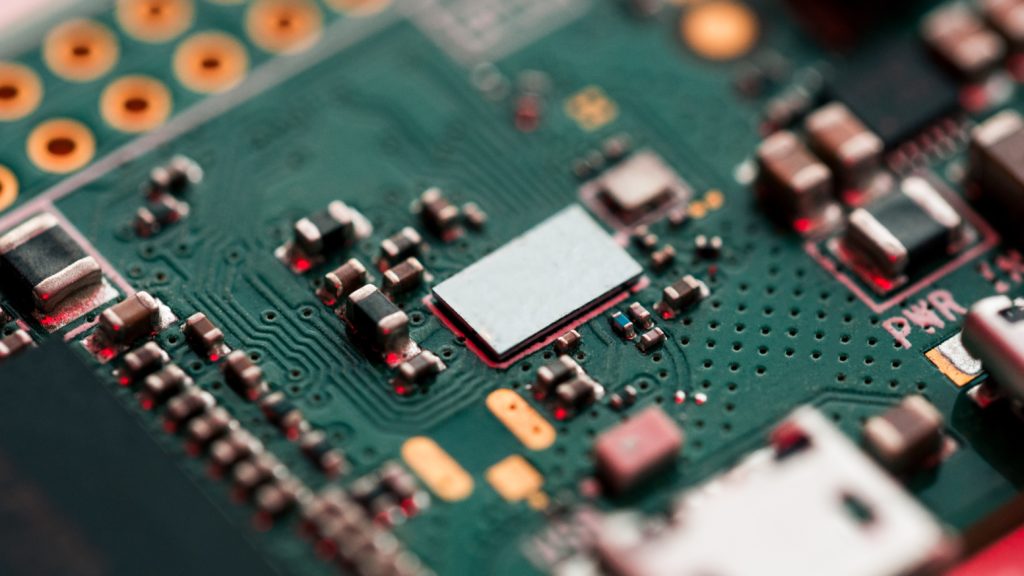
ASICs are also of different types, and the most advanced ASIC is the FPGA (Field-Programmable Gate Array). FPGA is not new to the semiconductor market and has played a crucial role in industry and academia. One of the advantages of FPGA is the ability to get programmed/configured to prove-in different methods and that too after manufacturing. It has thus enabled several industrial applications from audio processing to wireless communication to rovers on Mars.
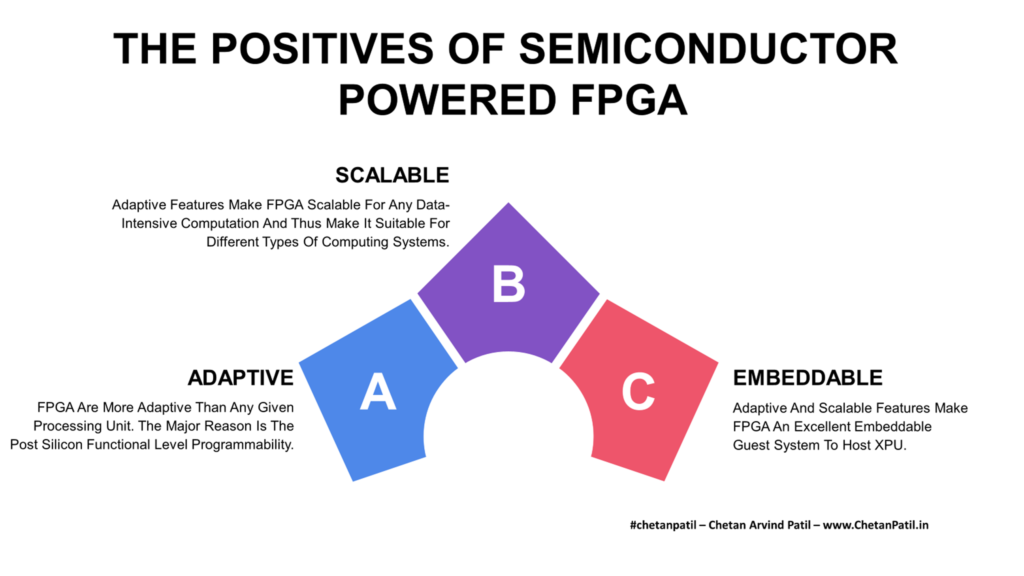
Adaptive: The design features of FPGA make it highly adaptive, and this provides the ability to deploy FPGA as per the target application requirements. It is possible due to the array of programmable blocks, which empowers developers to use (and also enhance) the FPGA as per the target application requirement.
Scalable: FPGA comes equipped with silicon features that enable them to be more scalable. Such features make them more adaptive than any traditional XPU. Such reconfigurability ability is possible due to the extensive libraries and IPs that the FPGA ecosystem has.
Embeddable:Several advanced computing systems often require dedicated ASIC that can take over the specialized task. This ASIC is often embeddable and comes equipped with the XPU system. In the same line, FPGAs are also embeddable and often carry out the specialized task on behave of the host system. FPGA being configurable are thus becoming a de-factor for the data learning world.
FPGA’s importance is growing further due to the adaptive/programming features that make it a perfect silicon for training a large amount of data on the go. ML/AI/DL is another area where FPGA has found a growing use. It is also one of the reasons why both Intel and AMD have invested billions of dollars to acquire FPGA-focused assets. These assets have enabled Intel and AMD to drive next-gen XPUs with embedded FPGA for specific post-manufacturing programmable requirements. Example applications can range from neuromorphic computing to inference-based processing to real-time metaverse.
Today, the FPGA market is approximately ten billion dollars. With the demand for real-time adaptive silicon increasing, the FPGA market will grow further and thus presents opportunities for both established and emerging XPU focused semiconductor companies.
The features of FPGA do not make it an alternative for traditional XPUs. One of the fundamental reasons for the fast growth of XPUs like CPU and GPU is the ease of use, and this is something that is not possible with FPGA due to the target application and the design/IP complexity.
However, in the last couple of years, the story has changed. Today, performance-oriented XPU comes equipped with FPGA (embeddable-FPGA or eFPGA). One important reason is to allow training/testing of learning algorithm on the device itself. Such silicon features are going to form the base for advanced X-Reality products.
Like any other computing system, FPGAs also have drawbacks. The majority of these drawbacks are not going to stop the growing FPGA market. However, overcoming these fundamental challenges can speed up the deployment of FPGA on critical infrastructure.
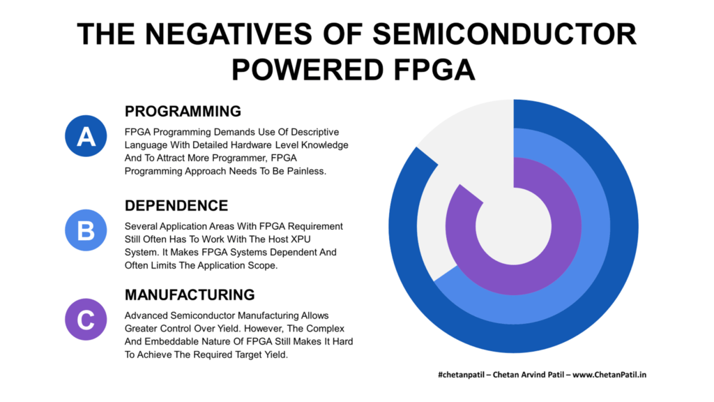
Programming: Programming FPGA is not easy and demands detailed in-architecture understanding. Companies developing FPGA often provide a set of software libraries and tools to make the programming experience easier. However, for the FPGA to become an attractive platform, the programming language needs to evolve. It might enable faster algorithm development to drive cost-effective solutions.
Dependence: There are several application areas where FPGA cannot get deployed without a host system. It makes them dependent on the host XPUs. FPGA developers have tackled this issue by utilizing low-power SoC, but the cost and complexity it comes with are high.
Manufacturing:FPGA is very complex, and embedding them with any other XPU makes the manufacturing process harder. Semiconductor manufacturing has advanced a lot, but driving high yield is still a big challenge for advanced nodes with highly complex designs like SoC FPGA. As FPGA becomes part of a more complex computing system, the manufacturing methodology will have to evolve too.
Neural Processing Units (NPU) are becoming a given feature for every new XPU. Intel, AMD, Apple, Microsoft, Qualcomm, NVIDIA, and several other companies are increasingly adapting their XPU to have NPU blocks. The building block of NPU is still FPGAs, and this makes it critical to overcome all the FPGA-related challenges to ensure the users can make the most of the FPGA ecosystem and are driving the adoption at a faster rate.
The semiconductor giants have already acquired long-term assets to make their XPUs FPGA friendly. These semiconductor companies are already delivering FPGA-inspired solutions and are pushing the computing industry to the next level. It showcases that FPGA will keep growing, and the semiconductor industry will keep coming up with advanced FPGA silicon.
Semiconductor wafers are fabricated and assembled to produce packaged semiconductor products before it gets shipped to customers. In the production, silicon product then gets mounted onto a system platform.
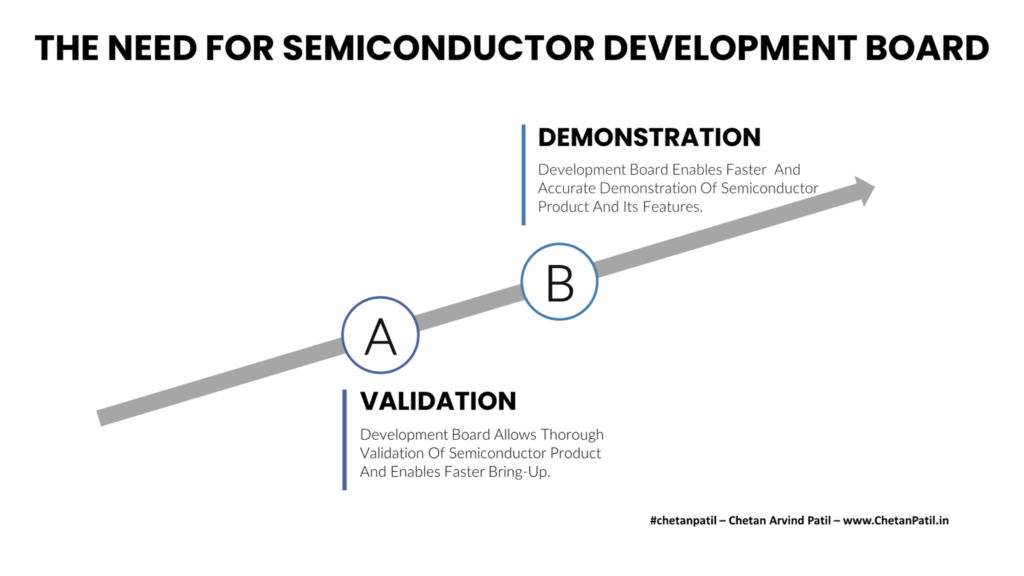
However, before the production line can use a semiconductor product, it needs to undergo several checks, which require a system-level platform calleda development board.
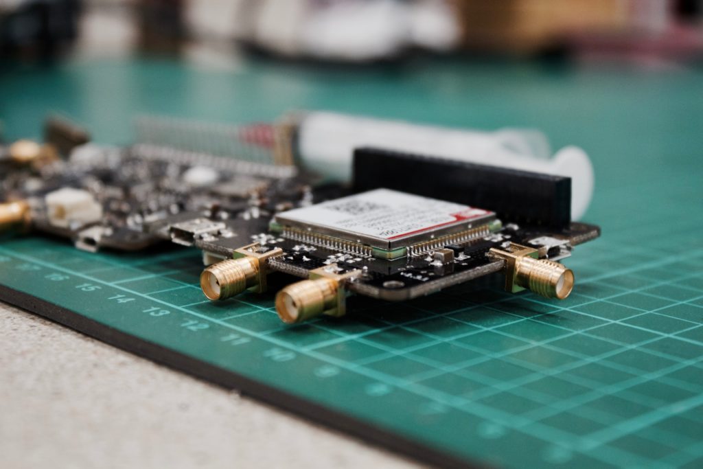
Development Board is a printed circuit board containing the main semiconductor product to be evaluated along with different support components needed to enable users to capture internal and external features of the target product.
Those interested in specific semiconductor products rely on the development board to thoroughly evaluate the capabilities of the silicon. Development board also provide a platform to electronic enthusiast and empowers them with options to test and build different semiconductor driven solutions. The Development board also ensures that the customer can capture the capabilities as promised in the datasheet.
Validation: Validation is the base requirement of any semiconductor product, and the development board provides such an option. Validation ensures that the product works as per the specifications, and it requires the semiconductor product to get mounted onto the development board. Doing so provides avenues to the customer to validate the end product.
Demonstration: Development board enables a platform to drive different demos. These demos give a quick evaluation of how the semiconductor product can develop next-gen solutions. During the consumer electronic exhibition, the development boards play a role by enabling demo of features that can potentially attract new customers.
Not all development boards get designed for the mass market. Several are for a specific purpose and used by the semiconductor design company and their customer only. Development boards for the mass market (Arduino, Raspberry, etc.) have been around for years and have always enabled new ideas.
In the end, the development board needs to have an impact on the end-user. It is only possible based on how good the development board is for evaluation purposes.
The impact the development board has on the semiconductor product defines how good the platforms can be. Not all products need a development board, but those which do should equip end-user with options to investigate the semiconductor product under evaluation.
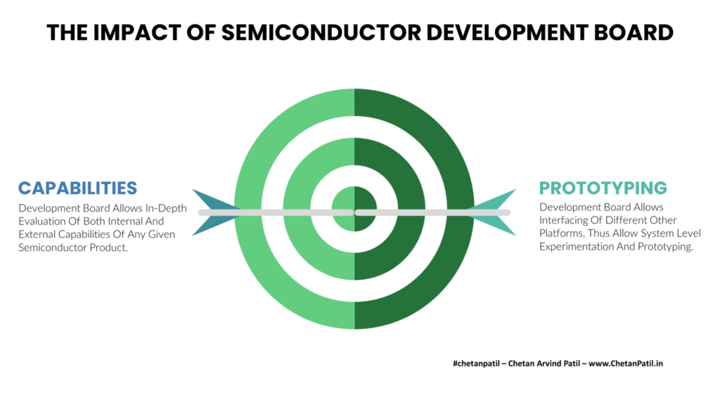
Several criteria can define how impactful the semiconductor development board is. Eventually, it all boils down to a couple of critical features that decide whether the development board can provide the much-needed hooks to capture end-to-end features.
Capabilities: A development board provides a detailed evaluation of the semiconductor product’s capabilities, and to capture all the features, it is crucial to provide all the necessary support files, guides, software, tutorials, and other details. Otherwise, the impact of the semiconductor product from its capabilities will be next to none.
Prototyping: All development boards have to comes up with features to drive prototyping. It requires the development board to come with peripherals that allow connection or communication to the next platform. Empowering prototyping also enables the testing of new and innovative ideas. Thus, the impact development boards have from prototyping is crucial too.
The main goal of development is to showcase the system-level capabilities, and it requires several other components to get mounted on the same target development platform. In the end, it becomes the evaluation of several semiconductor products, not just one. And, such an evaluation process is crucial as any production line always requires more than one silicon component to work together.
As several new semiconductor products (mainly on the processor and wireless communication side) come out in the market, the need for development boards will keep growing. New development boards with new semiconductor products also mean new options for the semiconductor market.
Semiconductor products are designed and manufactured for different conditions with varying requirements. These conditions and requirements are often a combination of several technical criteria.
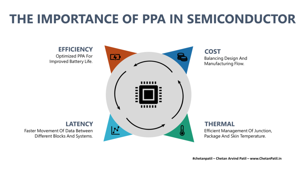
One such important criteria are Power, Performance, And Area (PPA).
In the end, the goal of developing semiconductor products is to provide as much functionality possible. This requires a perfect combination of PPA: Low power consumption with high performance in the smallest area possible.
The shirking transistor size has ensured that the die/chip area is not a technical concern when designing a semiconductor chip. However, at the same time, other technical challenges are posed by small die/chip areas. Mainly, balancing the power consumption while not affecting the performance.
Three-way balancing act of power, performance, and area (PPA) is becoming more challenging when the semiconductor products are used for applications that demand lower die/chip areas while also expecting higher performance. With decreasing die/chip area and increasing performance, the management of the total power consumption (static and dynamic) also becomes an uphill task. This leaves designers with limited knobs to play with. This is why considering PPA is important when it comes to developing semiconductor products with advanced technology-node.
There are four major factors that PPA can have an impact on:
Efficiency: There is not a single semiconductor product that is designed and fabricated to perform tasks inefficiently. The only goal of a smart semiconductor chip is to provide maximum efficiency. While 100% efficiency is not possible, the goal of PPA is to ensure there is minimal negative impact on the battery (given majority of the electronics system run on a portable battery system), and this is achievable only when the budget (during the design phase) takes into consideration how the performance and power scheme will be for a given die/chip area. There on building the full chip design becomes a more well-laid-out task.
Latency: Larger the die/chip area the slower the data traffic. This is more valid for XPUs, where N number of cores are working in synchronization to achieve the single task of crunching the data in the faster possible time. If the area is large and the layout is not optimized, then the latency introduced will be higher. On the other side, a large area (or even smaller in some cases) also has a far greater impact on total power consumption, while the performance is mostly on the positive side. This is another reason why balancing PPA becomes a critical task in semiconductor product development.
Thermal: Smaller the die/chip area, the less room there is to transfer the heat out of the system. This also leads to more static power consumption apart from the dynamic. On other hand, smaller area also requires advanced technology nodes that eventually mean higher junction and package temperatures (apart from skin temperature). This eventually demands smart dynamic thermal management techniques, which are only possible if PPA is managed efficiently.
Cost: In the end, the goal of any product (not just semiconductor product) is to optimize the cost of development. PPA plays a crucial role in cost too. Increasing die area can mean less room for more dies on the wafer, which means more wafers to product higher volume, and this eventually leads to higher development cost. This is another reason why PPA is an important factor when it comes to increasing product margin.
At the end of the day, the ultimate goal of the semiconductor product is to provide solutions that not only fit the market but are also the best version in the given category.
This is where optimizing PPA is vital, as it ensures the different functionality of the given die/chip is geared towards a product that outperforms any other competitor in the market.
Designers worldwide are always working towards the goal of achieving the required specification. This allows them to ensure that the semiconductor product is meeting all the criteria for the system it will eventually become part of. However, there are always design constraints, and PPA is one such vital constraint.
In reality, it is difficult to create a perfect balance of all the three components of PPA. One of the other parameters will always outweigh the other. This is more valid for critical semiconductor components like XPUs, which often demands less die/chip area for high performance.
Still, there are PPA driven bottlenecks that may hinder the success of the product:
Technology-Node: Balancing PPA does require choosing chip development technology that covers not only the product’s technical requirement but is also not costly to manufacture. Post design, the technology-node is going to stay with the product till the end of the product’s life. This is why PPA can many times drive technology combination choices that may not always be advanced. This may or may not have a major impact on the product’s success, however, PPA certainly adds constraint on the choice of technology-node.
Intellectual Property: The semiconductor design is getting increasingly driven by IP. This can be a bad news for the next-gen chip design as every new IP block might already have its PPA budget/scheme. This hinders the ability to play with the chip’s overall budget/scheme. This is why IP can sometimes introduce PPA bottlenecks in the chip designing process.
Memory: Memory is one of the most critical pieces of block in any given modern chip. More so when the chip is designed for workload-intensive tasks. The unpredictable number of reads/writes can through away the PPA budget for any given product. In such scenarios, it becomes difficult to count on the PPA budget scheme and often requires millions of simulations to validate the PPA scheme. This leads to bottlenecks on the design schedule and adds pressure to validate all the possible read/write scenarios.
Interconnect: If the area component of PPA has large say in the overall budget, then it can often lead to interconnected block systems that can introduce a lot of data traffic. This can have a heavy impact on-chip performance. This is often true for XPU based semiconductor chips. This is another possible way in which PPA introduces bottlenecks into the system.
As the semiconductor industry moves towards more advanced FETs, the importance of PPA will grow too. It can either lead to PPA schemes allow chips to outperform their predecessors or it can also have a negative impact (due to unbalanced PPA schemes). This is also one of the major reasons why new FETs and silicon chips are primarily focused on PPA to showcase the positive features of their new solutions.
In the long run, as newer FETs and technology-nodes get developed, both the semiconductor design and the manufacturing process will keep dealing with the act of balancing the PPA.
Every software application eventually has to get executed on a hardware system. Whether the software application is running on a smartphone or a data center, the data processing request has to get decoded (binary instructions) before the hardware system can process the request successfully. This seamless exchange of processes between software and hardware forms the base for a computer system.
Software form factor, user interface, and the speed might have changed over the years. However, the need to have a processing unit that can execute all the software code has not. Over the last two decades, the de-facto processing unit – the Central Processing Unit (CPU) – has seen several semiconductor and computer architecture backed technological advancement, that has taken computing to the next level.
As the software layers (application, presentation, session, and transport) are becoming model-driven (more pro-active, than re-active), so is the need to process the unique data/compute/memory intensive requests at the hardware-level.
Traditional CPU earlier was designed to handle a single request at a time. Then, the computing world moved towards multi-CPU (multi-cores) to cater to the parallel computing demand. Today, the de-facto is a System-On-A-Chip (SoC) that packs the CPU, the Graphics Processing Unit (GPU), and other processing units to process the high-resolution, high-speed, highly-data intensively requests in the shortest possible time.
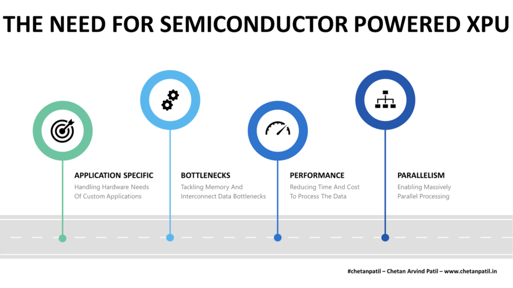
Semiconductor Powered XPU (X Processing Unit) Are More Application-Specific Than General-Purpose
The integrated system (mainly CPU + GPU on an SoC) has not been able to keep up with the computing world’s data processing demand. It has pushed the computer architects to design new types of processing units (apart from high-bandwidth memory, cache coherence, and smarter interconnect topology) that are more application-specific than general-purpose.
This race to come up with the new type of processing units has given rise to XPU:
X = Application Domain — Vision, Graphic, Neural, X-Reality, Video, Audio, and so on
P = Processing
U = Unit
XPU is different than CPU and GPU as it caters to the specific needs of the application. XPU is more application-specific, and it can work standalone or as a co-processor/co-unit alongside the CPU and GPU. XPU is geared towards throughput and speedy data management that takes the best out of the CPU and GPU design methodology to enable application-specific needs. XPU is not only Application-Specific Integrated Circuit (ASIC) due to the workload it is designed to cater to, but can also be classified asApplication-Specific Standard Product (ASSP).
The rise of XPU is enabling a new era in computing. The hardware and the semiconductor market are enjoying different challenges and solutions the XPU brings. Intel is betting big on it, and so is AMD. Apart from these two semiconductor giants, there are numerous innovative startups (and academic research) that have XPU powered solutions and are pushing the computing industry towards next-gen data processing.
Several types of XPU are available. It is vital to understand how these differ from each other apart from the two processing giants – the CPU and the GPU.
There are numerous XPU powered examples in the market. Many of these are still in a nascent stage and yet to prove the solution in the market. Given the growth and demand for new AI workloads, the XPU catalog will keep growing.
Below are the major semiconductor powered XPU:
AIPU – AI Processing Unit — AIPU is targeted towards an Artificial Intelligence solution and is mainly designed to cater to the Edge AI market. MediaTek Helio series of SoC is an example of AIPU integrated with CPU and GPU. Even RAIP – Real AIProcessing Unit (RAIPU), IPU – Intelligence Processing Unit or Image Processing Unit, EPU – Emotion Processing Unit – fall under IPU with the only difference being the change of name. The goal of AIPU, RAIPU, EPU, and IPU is the same – to process data to make a decision that is at-level or at-part with human intelligence.
APU – Accelerated Processing Unit — APU design requires fusing the CPU and GPU into a single die. AMD’s A-Series processor is a perfect example of an APU. APU is also capable of running a heterogeneous system by utilizing system-level architecture and software features.
AMPU – Analog Matrix Processing Unit — AMPU is designed to cater to the data training needs that are often large parameters that execute multiple matrix multiplications. AMPU custom feature to handle such parameters and matrix operations allows speedy training without relying on the external memory. MYTHIC’s Analog Matrix Processor is an example of AMPU.
BPU – Brain Processing Unit — BPU is envisioned to minim the human brain as it is. The processing unit is capable of performing multiple TOPS. Horizon’s Journey line of products is considered the first BPU ever and is designed in close collaboration with the Baidu Institute of Deep Learning. BPU may also form the base for Level 5 automation.
CPU – Central Processing Unit — CPU is the de-facto processing unit and is vital for general to specific purpose computing needs. Intel and AMD are leading the CPU innovation along with ARM. CPU is here to stay and will keep providing the much-needed multi-tasking capability for consumer applications. On top, Academia is still engaging in research to make cache and data pipeline more energy efficient.
DPU – Dataflow Processing Unit | Data Processing Unit | Data Parallel Unit — DPU focuses on speeding up the data movement between the cores and the memory. It requires a new interconnect topology apart from the smart placement of sub-blocks to minimize bottlenecks. The instruction set allows for faster memory and compute-intensive processing. Intel already several RISC (AVX512) instructions set to optimize processing for x64. DPU takes it to the next level with its highly optimized data pipeline, which enables massive parallelism. Fungible’s DPU is one such example apart from Deep Vision’s ARA series. RDPU – Reconfigurable Dataflow Processing Unit – is also a type of DPU.
DLPU – Deep Learning Processing Unit — A DLPU finds similarity with DPU. It is a domain-specific solution to enable faster training. DLPU finds use in Edge AI and similar applications. Researchers first showcase DLPU with DianNao paper, and recently in Cambricon-F paper.
GPU – Graphics Processing Unit – Like CPU, GPU has been in the market for a long time and is designed to cater to graphics applications. In the last few years, GPU has also found its way into AI/ML/DL applications too. Highly parallel design (with multiple core and large memory) of GPUs enables faster computation. GPU’s efficient programmability also allows faster training of dataset. NVIDIA by far is the leader in the GPU domain along with AMD, which is not far behind. Depending on how the GPU is fabricated in the computer system, it also gets classified as = DGPU – Discrete Graphic Processing Unit, GPGPU – General Purpose Graphic Processing Unit, EGPU – External Graphic Processing Unit, IGPU – Integrated Graphic Processing Unit.
HPU – Holographic Processing Unit — Coming out of Microsoft, HPU is designed for X-Reality. It incorporates design to process rich information that is generated by the sensors and cameras on the X-Reality device. HPU incorporates processing units to implement DNNs.
MCPU – Micro Controller Processing Unit — MCPU is not used to run operating systems or frameworks, but instead are geared to run Real-Time Operating System (RTOS) powered solution. MCPU find use in automotive, remote devices and even laptops desktop to offload non-critical tasks. ARM, Texas Instruments, and others have been providing MCPU solutions for a few decades. In the AI-powered world, the solution around MCPU is increasing, and architecture design is adapting to it.
NPU – Neural Processing Unit — NPU implements all the required blocks to enable faster data modeling using neural networks. Alibaba’s Ali-NPU is one such example. There are different types of NPU: NDPU – Neural Decision Processing Unit, NNPU – Neural Network Processing Unit, NDPU – Neural Decision Processing Unit. Eventually, the end-goal of the types of NPUs is the same – train the data faster using a neural network and framework.
QPU – Quantum Processing Unit — QPU is a computational unit that uses quantum computing principles to perform a task. The physics used in QPU is drastically different than the general-purpose CPU. D-Wave Systems is the leader in QPU, and their QPU follows superconducting computing. Google, IBM, and Intel have QPU based on a quantum circuit. QPU is massive and not designed for mass-market and are supposed to compete against AIPU.
SPU – Streaming Processing Unit — SPU is useful to process streamed data. The structured data enables placing the cores and memory to minimize the delay in bringing the new data to process. Google’s TSPU – Tensor Streaming Processing Unit – is an example of SPU. There are different types of SPU available in the market apart from TSPU: GSPU – Graph Streaming Processing Unit, TMPU – Texture Mapping Processing Unit, TPU – Tensor Processing Unit
VPU – Vision/Visual/Video Processing Unit — VPU is coming out in the market due to the demand for providing a rich visual experience. VPU consists of more video encoding and decoding units to enabled faster 3D processing. X-Reality is an application area where VPU finds use. Intel’s Movidius VPU is a perfect example of how to use processing units to process video applications with low-latency.
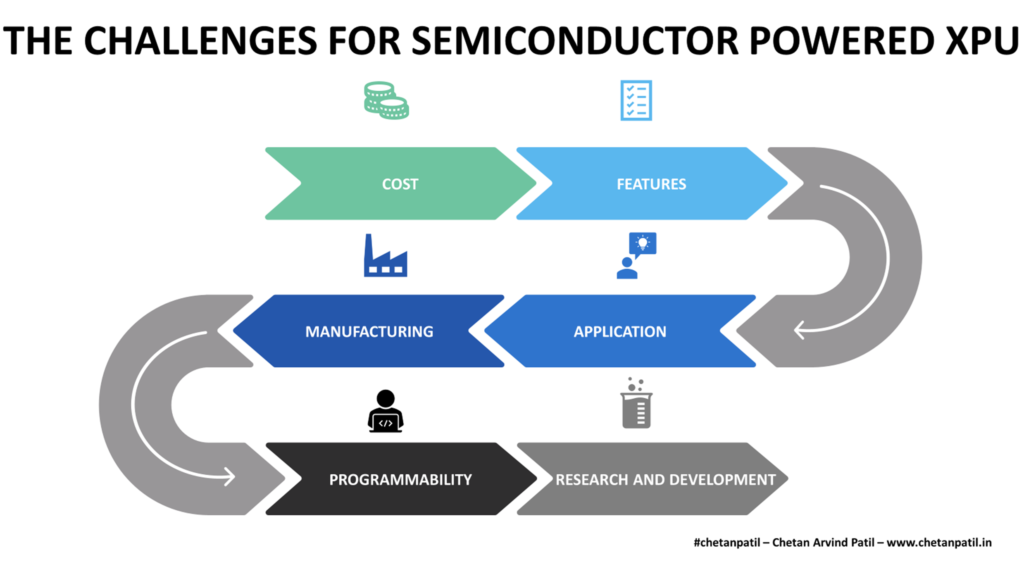
XPU is unique and solves niche problems. The challenges that come with it are many. Below are the hurdles and challenges that the semiconductor powered XPU face:
Cost: Designing a new processing unit not only enables new features to run the workload in the most optimized way possible. But it also adds the cost of design, development, and manufacturing. Balancing the CapEx is always the de-facto goal of any organization, and in the case of XPU, the stakes are higher given the stiff market competition. Companies looking to come out with more XPU based designs and solutions will have to make the process cost-effective to breakeven faster.
Features: XPU is feature-specific. Deciding which problem the XPU is going to solve is difficult to find. The semiconductor industry has launched different types of XPU that cater to almost all the possible computing domains and problems possible. Upcoming XPU will have to beat the existing XPU not only from the design point of view but also with respect to the features that make the new XPU sustainable in terms of power, performance, area, and cost.
Application: Defining use cases and features for XPU is another challenge. It requires figuring out the bottleneck in the existing applications/workloads and then designing the solution at the silicon level to solve it. TSU is one such example, which removes the bottleneck to train the data. Such a unique feature-based XPU is going to make it stand out in the market.
XPU Will Drive Innovation Along With General-Purpose Processing Units
Manufacturing: XPU either needs to be fabricated along with the CPU or as another block with the CPU inside the SoC or as a separate co-processing unit. In any of the three cases, it takes a unique semiconductor manufacturing process to ensure there is no process, quality, package, and reliability issues. Multi-Die Multi-Chip powered chiplets can be one way to ensure future XPU designs for manufacturability. The technology node and the packaging technology needs to be thoroughly tested before making the XPU with it. The goal of reducing the cost of manufacturing for XPU will be another challenge.
Programmability: Hardware is designed to run the software. Developing and running applications on any piece of silicon (mainly those designed to run operating systems and frameworks) requires the support of system-level libraries to ensure the data being processed can make use of all the internal features. Semiconductor companies developing different types of XPUs will have to provide APIs and system-level hardware interface libraries. This requires time and cost to develop. To keep developers engaged dedicated continuous API development teams are required. Providing such software features is vital and also a challenge to the XPU design team.
Research And Development: Continuous R&D is a vital factor that leads to a new type of XPU. It is critical to ensure that the R&D team can collaborate with academia to innovate new processing blocks. Organizing a dedicated top-notch R&D team is still a challenge given the competition in the semiconductor industry. Investment is another differentiating criteria when it comes to advancing new XPU designs.
It is an exciting time to be in the XPU domain. General-purpose CPU and GPU are here to stay, and along with XPU will enable a new, powerful and efficient way to solve the data problems.
However, the need to innovate in the competitive semiconductor industry will be the race to watch out. Companies like Intel, Apple, AMD, Microsoft, Google, Amazon, and Facebook will play a crucial role in pushing the market for semiconductor powered XPU solutions, alongside promising FAB-LESS startups worldwide.
The automotive industry is going through a significant transformation. Countries all over the world are pressing for greener and eco-friendly vehicles. Government policies are getting stricter and demand vehicular technologies that require smarter software and hardware.
The de-facto transformation is towards electric vehicles. However, other vehicular technologies (hybrid, autonomous, and alternate-fuel) are also driving the change in the automotive industry, and all this is pushing automotive companies to innovate. To keep up with the smart and safe automotive features, the share of software and hardware in automotive is increasing tremendously, thus leading to new automotive technology companies are also emerging. The emerging automotive companies work in collaboration with the established automotive companies or are launching their own smarter electric, hybrid, autonomous, and alternate-fuelautomotive products.
The Semiconductor Industry And Products Are Key To Developing Smarter Hardware To Drive The Automotive Industry Using Smarter Software
The need for semiconductor solutions in automotive is also pushing the innovation and development of smarter automotive chips to drive vehicles safely. The increasing need to develop error-prone software that runs on efficient hardware is vital and is driving the automotive industry to re-invent automotive solutions from a semiconductor point of view.
It is not that semiconductor products started getting used by the automotive industry in 2020. The automotive industry has relied on semiconductor products for decades. From airbags to infotainment and many other solutions have always required defect-free semiconductor products. However, the landscape of semiconductors in automotive is changing from individual silicon components to more centralized silicon systems. The semiconductor products work excellent for solo operations.
However, when the goal is to connect the system for level 5 autonomy or increasing hybrid efficiency, a centralized automotive-specific system-on-a-chip (SoC) is required. The centralized automotive semiconductor-based solution still relies on individual semiconductor components and is leading to innovative work from both the established automotive firms and the new semiconductor FAB-LESS companies looking to eat into the automotive and semiconductor market.
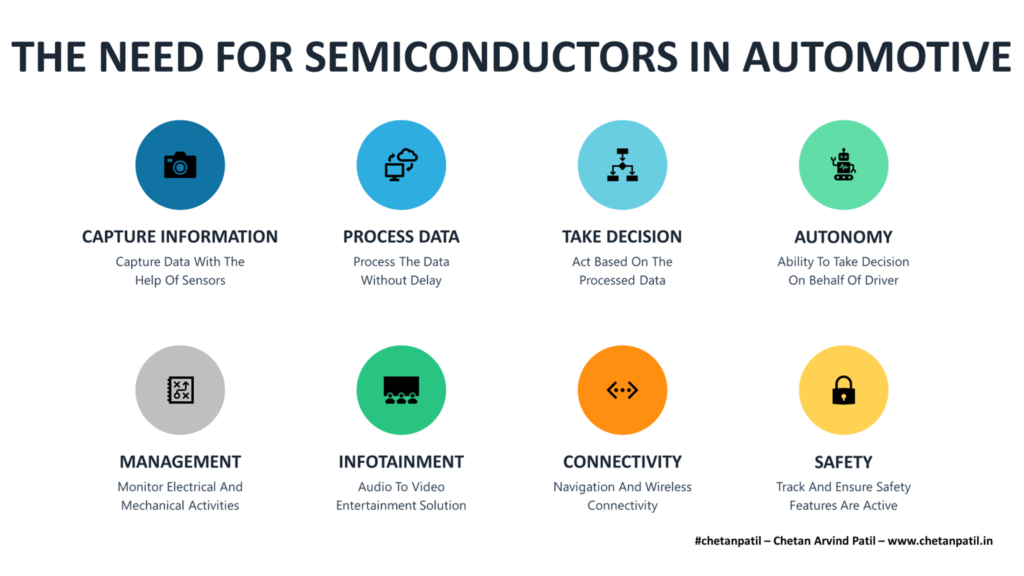
A centralized siliconsystem needs to cater to the following uses cases for autonomous automotive solution:
Capture Information: Ability to capture information with the help of monitoring sensors, LIDAR, and RADAR
Process Data: Information captured should is processed without delay
Take Decision: The processed data is used to take accurate actions
Autonomy: Decide on behalf of the driver to enable a safer experience
Management: Track electrical and mechanical activities to provide vehicle health
Infotainment: Display, audio, and video system for entertainment
Connectivity: On-the-go navigation, Bluetooth, 5G, and WiFi connectivity
Safety: Ensure critical components and features are working and alert when maintenance is required
The above use cases of semiconductors are valid for any kind of two/three/four automotive solution, including passenger, commercial, motorcycles, and industrial automobiles.
Developing semiconductor solutions for automotive requires strong collaboration with the semiconductor design and manufacturing industry. In some cases, the semiconductor solutions are also being developed in-house by automotive companies. It is why the automakers are investing or building R&D facilities to come up with a high precision silicon need for future vehicles.
It is critical to make use of a high-level intelligence system to make automotive products smarter. The growing share of technology-powered features in modern vehicles is prompting the automotive industry to invest in software and hardware capabilities in-house. In many cases, automotive companies are also collaborating and investing by out-sourcing many of the vital semiconductor solutions from silicon chips to sensors systems.
Hyundai: Hyundai has a long-term plan to remove the dependency on automotive products. In line with its vision, Hyundai has launched a semiconductor lab to develop semiconductor products for electric/hybrid vehicle powertrain controllers.
There are numerous examples of big automotive giants already owning or investing in semiconductor chip development. Given the decreasing cost of developing an automotive solution using advanced intelligence techniques, several startups and newcomers are also shaking the automotive market by providing semiconductor solutions.
New comers in automotivesilicon chip:
Autotalks: A FAB-LESS startup providing semiconductor solutions for vehicle-to-everything (V2X) communications for the automotive industry.
Tesla: While Tesla is not new to the automotive market, its silicon solution is certainly is. It aims to provide a silicon sandbox that is going to make any vehicle an autonomous one. Tesla AI chip is still under in-house use, but will certainly open up the market if sold separately.
Waymo: Owned by Google, Waymo, for now, is using Intel’s technology but in-house is also planning to develop its silicon chip.
The list of newcomers and startups in automotive semiconductors is going to increase. It will be interesting to see how the semiconductors market adapts to the solutions from the smaller companies.
It is for sure going to increase the importance of semiconductor design and development. However, there are still major challenges to overcome before automotive companies can make it big in the semiconductor industry.
Automotive companies which have been in the industry can establish the semiconductor business unit to meet its need. The challenges arise for newcomers wanting to cater to the automotive industry.
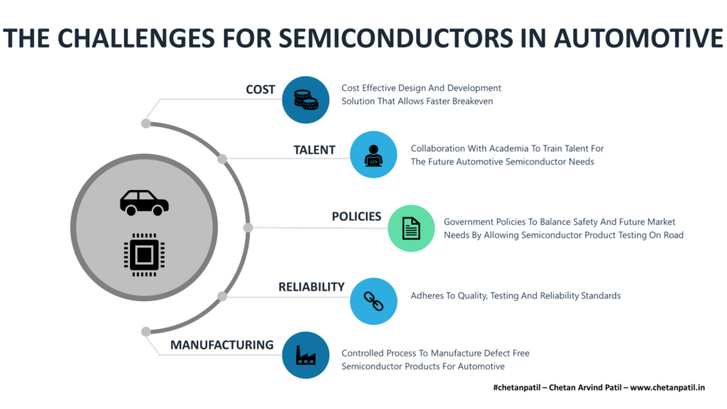
Five major challenges might hinder the progress of newcomers from providing elegant automotive semiconductor solutions:
Cost: Even though the share of semiconductor cost in new vehicles is on the rise, the challenge remains on optimizing the development and manufacturing cost to reach the breakeven point. Optimizing the process to make a low-cost product for large scale consumption is still a challenge. On top of it, proving the smarter semiconductor driven solution to the market is getting tougher. Autonomous (not specifically self-driving) technologies take years to test on the road before they can be used by the mass market. All this adds to the cost.
Talent: Acquiring relevant software and hardware talent to bring silicon solutions to bring innovation to the market is another challenge. Automotive companies getting into self-driving, electric vehicles, and alternate-fuel solutions are doing all they can to form the best team. In some cases, the practice is not as per everyone’s liking. Bringing new talents on-board and training them takes years too. Challenges also remain with universities to launch programs that cater to the new-age automotive and semiconductor market that requires different skills and demands. An interdisciplinary study that combines mechanical, computer, electrical, and semiconductor engineering is the need of the hour.
Policies: The lives of many on the road are at stake, and Government policies play a crucial role in the automotive industry. Not all countries or states enable the framework to test autonomous solutions out on the road. Dedicated infrastructure is required to test solutions like lane guidance and autonomous driving. It is difficult for states to grant permission to test the solution on public roads due to dangerous un-known consequences. Only a few examples of how state policy can strike the balance of technological progress and road safety. Arizona is one such example. The policy has to lead Chalder in Arizona to become the hub for self-driving design and development. Waymo to Uber to Cruise are all testing their solutions out on the road. It shows the growing need to make policies that strike the balance of safety and future market needs.
The Semiconductor Automotive Product Development Demands Talent Pool Trained With Interdisciplinary Curriculum Covering Mechanical, Computer, Electrical And Semiconductor Engineering.
Reliability: Semiconductor automotive products have to go through stringent qualification, testing, and reliability criteria. Automotive Electronics Council (AEC) and a few other standards provide the guidelines for qualifying the semiconductor products. The guidelines require the temperature to reliability stress testing. All these require resources, time, cost, and talent to execute. A chip not functioning during a crash can lead to fatality. Making automotive semiconductor product reliable is a key concern.
Manufacturing: Automotive semiconductor products eventually have to get manufactured in the same arena where smartphone semiconductor products get manufactured. A semiconductor FAB and OSAT have to ensure strict control over the process to ensure zero variation between lots of the same product. Controlling such requirement demands strong industry flow that enables defect-free products. FAB-LESS companies developing semiconductor products for the automotive industry have to engage and invest with semiconductor manufacturing teams.
The challenges are many, but so are the opportunities. Companies have to increase focus on semiconductor products in the automotive industry at the chip level. The automotive industry has leverage semiconductor solutions for decades.
The next decade is going to be a game-changer. The share of semiconductor products and costs in automotive is only going to quadruple. All this will open tremendous opportunities both for the semiconductor and the automotive industry.
Multi-Core Processor (MCP) or Chip Multi-Processor (CMP) revolutionized the computing industry. MCP/CMP came up with advanced execution and parallelism techniques. Software took the opportunity provided by the multiple processors fused into the single System-On-A-Chip (SoC).
MCP also provided the advantage of Out-of-Order Execution (OoOE), instructions-level parallelism (ILP), thread-level parallelism (TLP), and interleaved Simultaneous Multithreading (SMT), and allowed multiple applications to run on the same processor or multiple cores in the same SoC. Soon, the Single Instruction Stream, Single Data Stream (SISD) evolved into Multiple Instruction Streams, Multiple Data Streams (MIMD). MIMD gave a new experience to the data-intensive applications in the post-internet era.
The semiconductor and computing industry took advantage of MCP for over a decade by incorporating different core/processing units into a single SoC. Multi-Processor/Core System-On-A-Chip (MPSoC/MCSoC) became the heart of the new data and memory-intensive application. MPSoC/MCSoC starting to come up with dedicated processing blocks for data related to the graphic (GPU), digital (DSP), vector/vision (VPU), neural (NPU), and High-Bandwidth Memory (HBM).
The Artificial Intelligence System-On-A-Chip (AISoC) Is The Need Of The Future AI-Driven Workloads And Applications
The software computing industry is demanding data be processed faster than ever from semiconductor chips. Shrinking the transistor size further is not allowing the data and memory-intensive AI/ML/DL workloads to make the best of the MPSoC/MCSoC. Even though there are many opportunities to improve and innovate by proposing smarter data management techniques (cache, memory, and threading), MPSoC/MCSoC seems to have hit the memory wall, area wall, power wall, thermal wall, and performance wall. The data centers that should be shrinking in size and space due to the technology node advancement are instead becoming large by churning out massively distributed systems with a large number of MPSoC/MCSoC connected with large memory (NUMA).
The data-intensive, compute-intensive and memory-intensive artificial intelligence applications/workloads demand SoC that is:
Low Cost:
Affordable to manufacture
Efficient:
Improved performance-per-watt (PPW)
High Parallelism:
Massively parallel execution without stalling
Smart:
Ability to generate/store/predict models on the go that reside closer to the cores
Zero Bottlenecks:
Processes the data without memory/interconnect bottlenecks with or without a co-processor
Adaptive Software:
Ability to get programmed with minimal high-level programming effort and adapts on the go
High-Speed Memory:
Provides a large amount of high bandwidth memory across different memory levels/hierarchies
Technology Node:
Works efficiently irrespective of the advanced technology nodes used
The above eight-point feature is what will pay the way for Artificial Intelligence System-On-A-Chip (AISoC). These AISoC will be critical for the next generation of advanced solutions that will find use in the growing autonomous world. AISoC can be used in all devices and not only in the data centers. AISoC can speed up the fast-changing automotive to the satellite industry.
To cater to the growing demand for the semiconductor SoC chips for Artificial Intelligence) and to also balance the complexity, cost, and time to market, the semiconductor industry has already started to move away from general-purpose cores to specialized cores.
While the semiconductor industry is not labeling these new SoC as AISoC, but the features offered are of the AISoC world. Not all the AISoC solution adhere strictly to the eight-point features discussed above, but the solutions offered by different semiconductor companies is a step in the right direction.
Leadership in AI semiconductor chips is vital. Countries across the world are competing to bring the best homegrown solution to establish the lead. Governments are also funding the semiconductor chip business with the hope of leading the semiconductor race and mainly the AI solution one.
Apart from governments, companies across the globe are also racing against each other. From software giants to hardware leaders, all companies are investing zillions of time and money to come up with AI semiconductor chips out in the market.
The Artificial Intelligence System-On-A-Chip (AISoC) development is happening in two parallel worlds:
Established companies building in-house AI semiconductor chips
Startups providing a new architectural solution to drive AI semiconductor chips market
Below is the snapshot of the world’s top established companies racing against time to bring AISoC not only for their consumption but also for the market:
Alibaba: Alibaba competes directly with e-commerce giants and mainly Amazon. It provides web services similar to Amazon Web Services. To cater to enterprise needs, Alibaba last year launched Hanguang 800 is capable of processing 78,563 images per second. Alibaba introduced XuanTie 910 in 2019 provides 40% more performance than reference ISA RISC-V. These two AISoC are only a handful of examples. Alibaba’s DAMO Academy is continuously innovating and is going to launch much more surprising products in the AISoC domain.
Amazon: Amazon caters to more than 200 million visitors per month. Every visitor provides Amazon business and also the data on his/her shopping behavior. To process and make use of such unique data and to also provide enterprises the efficient web services, Amazon has been investing in AI-driven chips for a long time. Amazon’s Inferentia is the first step towards conquering the server market that is AISoC powered. The growing Alexa line of products pushed Amazon to in-house AISoC development and the results are already been seen in form of smarter voice-assisted devices.
AMD: AMD is another established semiconductor company with AISoC products. With AMD Instinct and AMD EPYC line of products, AMD has been steadily growing its market share in AI-enabled devices. AMD is also making most of the semiconductor chiplets technology to bring more innovation at the silicon level. Its acquisition of Xilinx is only going to help bring more AISoC solutions to the market. AMD is not deep into the mobile space, but they can certainly take advantage of the growing gaming industry to compensate. AMD CDNA is also another breakthrough architecture design to speed up high-performance computing.
Apple: With the launch of M1, Apple has shown the world its next target is going to be more in-house Macbook and iPhone/iPad processors. M1 has a NPU that allows faster predictive actions for its users. Apple is also planning to launch X-Reality products, which will require elegant AISoC, for which Apple has already started the work.
ARM: ARM IP has been critical for the smartphone industry and has taken the lead in providing AI-powered chips for mobile and also the data centers. With TOP500 won by ARM-powered supercomputers, ARM is ready to come up with more AISoC solution. Smart homes, wearables, and smartphones will see a massive use of AI Chip that will be powered by ARM. With Apple going all-in for ARM processors, and it will also help ARM innovate on the AISoC front.
Infineon Technologies: Infineon Technologies is going big in the AI Chip domain. It has established an AI development center in Singapore and also has a series of MCU designed with AI in mind. Low-cost MCU running with AI capability is the perfect solution for portable smart devices like cameras, drones, and smart speakers. AISoC with inbuilt MCU is another avenue Infineon is capable of exploring.
Marvell Technology Group: Marvell has launched a series of ASIC-based accelerators to cater to the AI data demand. The custom ASIC solutions used high speed interconnects and innovative packaging to optimize performance and cost. On top, Marvell has a strong collaboration with TSMC to provide 5/7/14 nm AI ASIC that allows it to pitch a wide range of portfolio to the growing AISoC market.
Qualcomm: As mobile AI is growing, Qualcomm is taking advantage of it by providing On-Device AI accelerators. Qualcomm has also taken steps towards a cloud AI Chip solution. It launched Cloud AI 100 chips to showcase its new architecture design for AI and data centers. Stronghold on mobile business with already out AI chips, Qualcomm can spring a surprise and enable new data centers that are not only AI-enabled but are also low-power and efficient AISoC.
Samsung: Samsung has fingers in many pies. From the design of chips in-house to the capability of manufacturing chips for its products and the world. Like Qualcomm, Samsung has been pushing for an AI chip to enabled On-Device AI. It has also collaborated with Baidu to develop a server-class of AISoC. The advantage of owning a foundry allows Samsung to innovate end-to-end and will be vital to see if it goes in the data centers’ AISoC chip design and development.
Texas Instruments: Like NXP and Infineon, TI is also providing Edge AI chips that cater to the 5G market. TI’s manufacturing capability fueled with low power techniques is going to provide a way forward to the industry on how to innovate AISoC with low power consumption.
The above summary shows how established companies are innovating and launching AISoC. The cost to establish a FAB-LESS semiconductor startup has gone down. The advanced EDA tools provide the ability to test ideas in the shortest possible time. RISC-V open ISA is also helping innovate without investing in royalty based ISA.
All this has lead to an increase in the number of FAB-LESS semiconductor startups that are coming up with new semiconductor chip designs and solutions to cater to the AISoC market. These startups have already got traction and some are even collaborating with established companies to test the solutions.
Below is the list of some of the top startups coming up with silicon level technology to drive AISoC design:
AlphaICs: AlphaICs is focusing on Edge AI and has designed an AI Processor that finds application as both the mobile and the data center solution. AlphaICs call their AISoC as Real AI Processor (RAP)
Alphawave: Alphawave provides Digital Signal Processor (DSP) solutions that are suited for high-speed performance and are low on power consumption. DSP provides audio/video processing and with Alphawave’s AppolloCORE IP semiconductor companies can build AISoC with an onboard accelerator. Alphawave was also the winner of TSMC’s Awards for Excellence in Accelerating Silicon Innovation
EdgeQ: EdgeQ is taking a different approach to Edge and 5G by fusing both into a single AI-powered chip. This will massively off-load the tas from data centers to Edge Computing. With 5G rollout already in progress worldwide, the solution is at the right time for the right market.
Horizon Robotics:Journey and Sunrise processor architecture from Horizon Robotics is designed to provide an AI-enabled Brain Processing Unit (BPU). Journey BPU is designed for the automotive industry, while Sunrise is for the IoT market.
Both established companies and startups are showcasing the world’s new way to design chips and drive data processing. All this is making software development, training, testing, and data analytics faster. The AISoC from all these vendors is also providing avenues for low-cost AI-powered mobile and data centers.
The majority of the challenges the AISoC face are still the same old problems faced by general-purpose CPU and GPU as the technology at the silicon level advanced. The new AISoC solution from both the established companies and startups are eventually going to hit with these challenges.
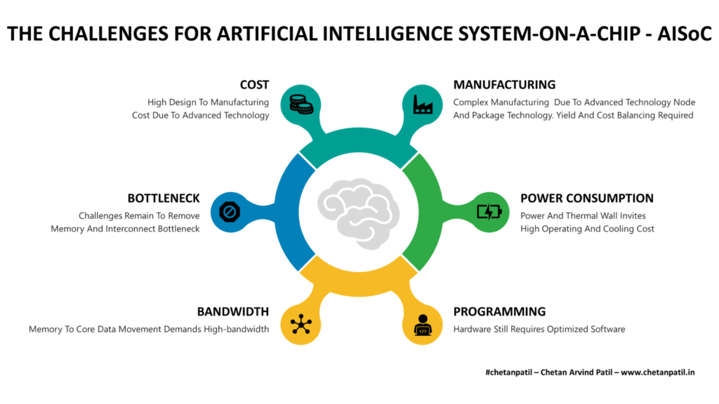
Cost: Designing and establishing AISoC proof-of-concept using the software simulator demands resource and pushes the cost of development from FAB to OSAT. The cost of owning smartphones and running data centers is already high. On top of it, any new solution with AI-power will add cost to the customer. The technology node required to enable a high number of processing units to speed up the training and inference is eventually going to cost money. AISoC vendors need to balance the cost of manufacturing in order to breakeven the market. On top of all this, the amount of competition in developing new AISoC means time to market is vital than ever.
Bottleneck: The reason to move away from general-purpose CPU and GPU was memory and interconnect bottleneck. There are few startups listed above that are trying to remove these bottlenecks. However, with the speed with which new AI-workload are getting generated, there is a high chance that bottlenecks will still exist. It will be vital to ensure that the new type of AISoC that both the established companies and startups are envisioning does not have any bottlenecks.
Bandwidth: Bringing the data closer to the processing units (any type) is the key to processing AI data faster. However, for such a task high-speed memory with large bandwidth is required. The new AISoC are incorporating new processing units like RAP, GSP, TSP, BPU, AMP, RDU, NDP, and so on, but there is no clear strategy and details on how the data communication bandwidth is improved. May be such details are proprietary.
Programming: In the end, any AISoC cannot process the data efficiently if the workload is not optimized for the target architecture. While few AISoC is pitching their products as no need to change the data or framework before running it on their architecture, however, the reality is that every architecture ends up needing some or other form of optimization. All this adds to the time to develop data solutions.
Manufacturing: As the new AISoCs come out in the market, many of these will end up using advanced nodes beyond 7nm to provide high speed. Advanced packaging technology also is required to operate the AISoC within the thermal budget. Both the complex technology node and package technology will drive a high manufacturing cost. Apart from this, balancing yield and cost will be essential to ensure AISoC development is viable.
Power Consumption: AISoC requires zillions of transistors that require faster cooling. The majority of the AISoC can do with liquid cooling but when such AISoC is connected together to form data centers then the cost to run data centers goes high. Hopefully, greener technologies will be able to run such data centers. However, the AISoC will get challenged to overcome the area, power, and thermal wall.
No matter what, AISoC in coming years is going to be the semiconductor domain that will innovate and provide elegant semiconductor solutions that will challenge the end-to-end semiconductor design and manufacturing.
Internet usage is growing. Every new user generates a new type of data. The technology companies are always eager to process and understand new consumer behavior. It requires continuous research and development of both the software and the hardware.
Software development has advanced in the last two decades. It has kept pace with the need to understand and process data due to the development of software libraries and frameworks. The large amount of data that has generated post-2010 has helped the Deep Learning (DL), Machine Learning (ML), and Artificial Intelligence (AI) frameworks train networks, and that is now allowing new data to be processed faster and accurately.
Hardware is vital in ensuring that the processing of data using training and prediction frameworks occurs in the shortest time possible. It requires a massive amount of computing. The majority of the technology companies now rely on massive data centers equipped with advanced computer architectures.
BIG-5 – Facebook, Amazon, Apple, Microsoft, Google – FAAMG
To fully utilize computer architectures, an in-depth architecture-level understanding is required. It is not always possible to do so, as the data centers still run general-purpose computer architectures that do not cater to different types of data the big technology companies have to process.
The disconnect between the software, the hardware, and the data has promoted the need to move from General-Purpose SoC To Application-Specific SoC. Not all data companies are capable of setting up a dedicated team that can focus on in-house silicon development to come up with an Application-Specific SoC.
To overcome the reliance on semiconductor companies, the BIG-5 (FAAMG) technology companies have started (or have already developed) developing in-house SoC with the hope of opening up the silicon to different data companies around the world.
Two major factors drive the push to develop new computer architectures (silicon):
Memory
Parallel computing
Memory:
Modern applications are becoming memory intensive and also demand faster computation. To process requests from memory-intensive applications in the shortest possible time, the data needs to reside closer to the processing unit.
The time to bring the data from SSD to DRAM to Cache adds cycles and delays processing of the data. To overcome such bottleneck, semiconductor companies have implemented the following three techniques:
Cache Prefetching:
Bring the data near the processing unit in advance to minimize cycle time
Increasing Level Of Cache:
Add Leve-1 (L1), Level-2 (L2 – Shared), and Level-3 (L3 – Shared) small (KB/MB) cache memory to improve memory prefetching speed
Enable High Bandwidth Memory:
An extra layer of large high-speed memory between Last Level Cache (LLC – Either L2 or L3) and DRAM to speed up prefetching
All the above three techniques improved the response time of processing units. However, as the application data started growing, the cache and memory trashing became a new hurdle.
Multiple processing units sharing the same level of memory started corrupting each other’s data to process the request faster. On top of all this, the lack of interconnect bandwidth added further bottlenecks.
Parallel Computing:
Apart from being memory intensive, applications have become compute-intensive too. It prompted the need to have multiple processing units within the same SoC. Running multiple data requests on a single processing unit or two separate processing units provided a way to accomplish the task in the shorted possible time.
The processing units still relied on the low-level memories to bring the data to be processed quickly. It means new SoC designing techniques that can allow the sharing of cache and high bandwidth memories in elegant ways without compromising on the need to add latency.
Adding more processing units to a single SoC is not the solution. On top, the developers have to keep comping up with smart ways to distribute the data to multiple SoC to speed up the processing.
Distributed computing is what the majority of the technology companies have adopted to ensure the data is processed quickly. It means a massive number of servers with thousands of SoC and a large amount of memory. Over time this has increased the cost of operating data centers.
Even though in the last decade, semiconductor companies have come up with unique computer architecture to cater to both memory and compute-intensive applications, it has not been enough to adopt the changing processing requirement of BIG-5.
The need to handle memory and parallel computing demand by modern workloads and applications efficiently at the architecture level has pushed BIG-5 to go for in-house silicon.
THE STATUS OF IN-HOUSE SILICON
BIG-5has been gearing towards the development of adaptive computer architecture for data and operating systems.
They have a silicon team that is focusing on Application-Specific SoC development that not only caters to data centers but also portable devices like Oculus.
Amazon:
Amazon Web Services (AWS) is one of the leaders in cloud solutions. The desire to have customized SoC is vital to ensure the consumers and enterprises can make most of the wide range of computing services AWS provides.
Apart from AWS, Amazon’s growing range of Echo products is also pushing it to drive in-house silicon development. Amazon is betting big on ARM architecture to drive its silicon needs.
Microsoft always had a keen interest in hardware. They already have a strong team of researchers focusing on hardware research. The Surface line of products has shown strong growth, and the SQ1 line of SoC establishes Microsoft’s goal of making Windows smoother to use on silicon.
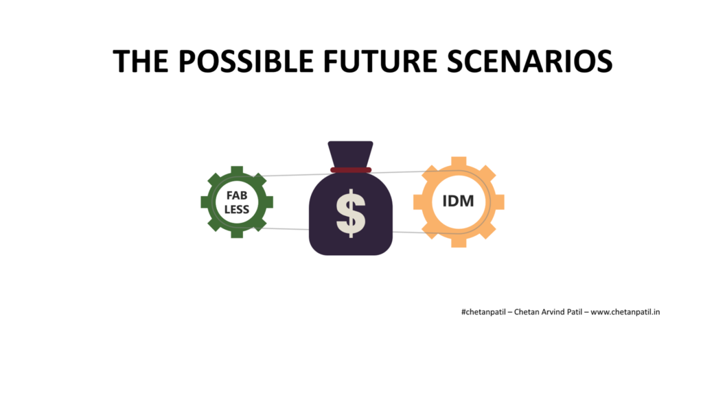
BIG-5 is betting big on in-house silicon development. This requires not only years of planning and investments but also a dedicated semiconductor development team and flow chain. Going forward there are two possible scenarios that BIG-5 might take:
Scenario 1:
BIG-5 will keep collaborating with semiconductor companies (Intel, ARM, AMD, and Qualcomm) to design silicon for their products and data centers with strict control over features and the manufacturing process. It will enable BIG-5 to enter the in-house FAB-LESS business model.
Scenario 2:
BIG-5 will slowly move away from semiconductor companies and spin-off an in-house team with a full turnkey silicon development chain. It will be more like an IDM business model and might require the acquisition of existing semiconductor manufacturing units.
The probability of the second scenario occurring soon is unlikely. In a decade or so, BIG-5 may go big on the semiconductor business and try to keep themselves as in-house FAB-LESS silicon developers (while owning a piece of IDMs/FABs), which will ultimately play in the hands of FAB/Pure-Play Foundries like TSMC and GLOBALFOUNDRIES.
Whichever scenario ends up occurring, there will be exciting developments in computer architectures that will drive the semiconductor industry to new levels.
Computers are designed to provide real-time feedback to all user requests. To enable such real-time feedback, Central Processing Unit (CPU) is vital. CPU is also referred to as processing units or simply processors. These incredibly small semiconductor units are the brain of the computer and are capable of performing Millions/Billions of Instructions Per Second (MIPS/GIPS). High MIPS/GIPS, means faster data processing.
A lot of processing goes on inside these processing units. With the advancement of the technology nodes, more processing units are being glued together to form System-On-A-Chip (SoC). These SoCs have different individual units like GPU, DRAM, Neural Engine, Cache, HBM, ASIC accelerators, apart from the CPU itself.
It is incredibly difficult to design an SoC that has the best of two important worlds of computer architecture: Power and Performance.
Both in academia and the industry, Computer Architects (responsible for design and development of next-gen CPU/SoC) play a key role and are often presented with the challenge of understanding how to provide faster performance at the lowest power consumption possible. It is a difficult problem to solve.
The battery technology has not advanced at the speed at which SoC processing capability has. Shrinking technology node offers opportunities to computer architects to put more processing power, but at the same time, it also invites issues related to the thermal and power budget.
All this has lead to semiconductor companies focusing on design challenges around the power and performance of the SoC.
CHALLENGES
Semiconductor industry has been focusing on two major SoC design challenges:
Challenge 1:Efficient and low latency SoC design for portable devices
Challenge 2:High throughput and performance oriented SoC for data center
Portable devices suffer from the constraint on the battery capacity. The battery capacity has been increasing mainly due to the shrinking board inside these devices due to the shirking transistor size.
This has allowed the OEMs to put more lithium-ion. However, to balance the form factor and portability, batteries cannot be scaled out forever. It is a challenge for OEMs to understand how to manage portability by balancing the battery size apart from making the computer system efficient with low latency.
Efficiency And Low Latency
To tackle efficiency and low latency, innovative designs are coming out in the market with the ability to adapt the clock and voltage domain depending on the application being executed by the user. It is no more about how many cores are in the SoC, but more about how an application-specific core can provide a much better user experience than ever.
This has presented researchers with an interesting problem of improving the performance per watt (PPW). To improve PPW, researchers around the globe are taking different approaches around DVFS schemes, apart from improving transistor level techniques.
Frequency and voltage level scaling also has a direct impact on the response time. Processing units like CPU are designed to provide low latency so that all the request coming in, can be catered to in real-time.
Improving efficiency without compromising on the latency is still a big challenge for the computer architects.
Challenge 2:
Data Center:
On the opposite pole, data centers are designed to be compute-intensive. The SoC required to cater data center has exactly the opposite need compared to portable devices. As companies become data aggregators, the analysis requires dedicated hardware that provides streamlined computation of the data on the go.
This is prompting companies like Google, Facebook, and Amazon to come up with their silicon that understands the data being generated and how to swiftly analyze it on the go.
Performance And High Throughput:
Designing custom SoC requires a fresh look and is drastically different than the block based approach. Improving throughput requires high speed interconnect to remove bottlenecks in data processing, else the performance will be affected.
In order to improve throughput, the data needs to reside near the computation block. This demands a new way to predict data to be used in order to bring in the cache or add a memory hirerachy with the help of MCDRAM.
The challenges are many and researchers around the globe are already working to provide elegant computer architectures both from academia and the industry.
WAY FORWARD
As the need of the application running on the computer systems is changing, so is the approach to designing SoC. Various examples from different companies show how the development of computer architecture is changing and will eventually help others come up with new computer architectures.
These new architecture designs are taking the traditional approach of computer architecture and providing a different way to tackle both memory and compute bottlenecks.
Cerebras came up with Wafer-Scale Engine (WSE), which is developed on the concept of fabricating full wafer as a single SoC. The performance data of WSE show a promising future of how computer architecture becomes more wafer-level designing than die level. WSE also takes different approach on interconnects by utilizing wafer scribe lines to transfer data which provide more bandwidth.
Fungible’s Data Processing Unit (DPU) architecture is another way forward that shows how SoC will be increasingly get designed for scale-out systems to handle massive data.
Google’s TPU and Amazon’s Inferentia shows how custom ASIC based SoC will become de-facto. Companies that generate a lot of data will try to run their center on in-house developed SoC.
Apple’s M1 launch showed how ARM will start eating the x86 market for energy-efficient portable devices. In few years, the integration will become more intuitive and might attract other x86 portable devices OEMs who have failed to take Windows on ARM to its true potential.
NVIDIA’s bid to acquire ARM shows that the future GPU will be designed with a blend of fusion technology that will combine ARM/CPU with GPU more than ever. This will allow data centers to improve on latency apart from focusing on throughput.
In the end, all these are promising development for the computer architecture community. Provides numerous opportunities to research and develop new ways to enable lower latency and higher throughput while balancing power consumption.
Apart from the steady increase in design, development, and production, merger/acquisition have gone up too. There have been some unexpected takeovers which are bound to have a strong impact in the long run.
The semiconductor industry from a product point of view can be divided into:
All these acquisitions from the design have shaken up the semiconductor design industry. However, at the same time, it is turning out to be a boon for semiconductor manufacturing, as many IDMs plan on becoming FAB-LITE to focus more on the design aspect and increase share the mobile, AI, and data center market.
This raises the question of how the future of semiconductor design and manufacturing is going to be.
THE SEMICONDUCTOR INDUSTRY SHAKE UP AND FUTURE
Taking a look from the semiconductor design point of view, it is getting clear that companies are more focused on a specific product domain and want to dominate the market. To achieve this, companies are either creating new asset via acquisition or selling old asset that do not align with the goal.
Intel last year sold its smartphone modem business to Apple and this year Intel also decided to sell NAND memory business. This shows that Intel wants to focus on its strength of personal and data center computing. For sure, NVIDIA’s acquisition of ARM is concerning for Intel, given how much strength an established IP from ARM will give NVIDIA and also allow it to extend its business from GPUs to CPUs, and that too smartphone business which is not Intel’s primary domain.
On top, with AMD’s solid performance and acquisitions, the fight for smart computing is going to heat up. AMD (since 2009) and NVIDIA are FAB-LESS semiconductor companies. This allows AMD and NVIDIA to focus more on the design aspect and let external manufacturers take care of the manufacturing. This is a big advantage as semiconductor manufacturing is hard and takes a long time to perfect.
All these points towards a major shake-up that will occur in near future. The business mode; will change and semiconductor companies will go either:
FAB-LESS
FAB/Pure-Play Foundry
Competing in both the arena as a single entity is going to be challenging. Spinning off or selling part of the semiconductor manufacturing might be a more viable solution. Such shake-up will eventually end up creating more business for the semiconductor manufacturing companies and they will have to predict today and start planning on increasing the capacity (or acquisition) to keep the business running.
It will be vital for countries like India to take advantage of such market business change by coming out with policies that heavily incentivize semiconductor manufacturing.
The software business delivery model has been constantly changing. It has adapted the need of the market by leveraging all the possible ways to deliver the software solution hassle-free. From installing software using a CD-ROM or USB Flash Drive to installing over the internet, the ease of accessing and using software has changed a lot.
The customers have also adapted to the changing landscape. From worrying about configuring the license key correctly to transitioning to subscription (monthly/yearly) model has provided numerous benefits.
One major change in the software delivery model has been the cloud services, which has pushed the applications from the desktop to the browsers. This has greatly eliminated the need to configure the operating system and environment settings required to ensure that the application works flawlessly. Today, with the click of a button, one can securely log on to the website and access the software tools using any browser without worrying about the underlying operating system.
While the software has certainly made great progress, hardware has not been behind. The sole reason one can access software tools remotely is that the data centers located in the different parts of the world are working in harmony. This is to ensure that all the requests are processed with zero downtime and minimal delay. The underlying network of hardware ensures that, low latency is not a hindrance in accessing the software features. This has removed the need to maintain self-hosted servers and has allowed customers to instead invest in other critical solution to make the day to day task more productive.
The software licensing and delivery model today is termed as Software-As-A-Service (SaaS). It is a subscription-driven model where the application is hosted on a server and can be simultaneously accessed by all the subscribers without any resource constraints. The server will have all the software dependency pre-configured to let the developers focus on the delivery.
To run the SaaS model, a set of hardware tools are required. Instead of spending millions of dollars on the hardware infrastructure and maintenance, many enterprises and solution seekers have moved to the hardware licensing and delivery model and it is termed as Hardware-As-A-Service (HaaS).
The major difference between SaaS and HaaS,is the application. SaaS is primary all about software, while HaaS is not just about computer hardware and system but also about all those smart hardware solutions that are running the SaaS.
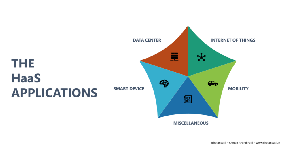
THE HaaS APPLICATIONS
The application areas of any given product is what differentiates it from competitors. In the last decade, the HaaS application has increased and many smart hardware providers have moved to the product-based service model.
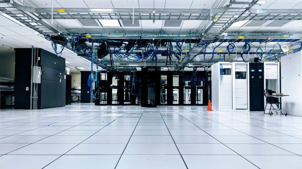
The important application area of HaaS has been the data center, where cloud service providers (Amazon, Google, Microsoft, etc.) and content delivery networks (Akamai, Cloudflare, etc.) have created plethora resources to cater the growing need and demand of software enterprises. Anyone can rent as many nodes required and deploy a solution. The shared and dedicated website hosting also falls into the same category. Renting out per month basis than buying the hardware and setting up in the office is more cheaper and reliable. HaaS (Hardware == Data Center) also eliminates the cost of setting up a dedicated team to handle all the data center related issues.
The growth of smart devices has lead to change in the way consumers consume these products. Taking the queue from the smartphone business, it is evident that a new version of the smartphone is launched every year. This automatically prompts consumers to buy a new one due to the attractive features. Shelling out more than $500 every year on a smartphone is not what every consumer would like to do. To tackle this issue, the service providers (mainly cellular one) moved to the HaaS model (Hardware == Smart Device), in which they started providing the smartphone as part of a monthly plan than paying upfront. It certainly has pros and cons, but has provided consumers the ability to switch to better devices as and when required. This smartphone subscription model is now being extended to several other smart devices like cameras, drones, watches, security, T.V., and the list is endless.
Mobility is a very crucial part of the day to day life. In the transportation area, the HaaS model (Hardware == Vehicle) has been in use for decades. The model of renting the vehicle for a specific period is well proven and widely used. Due to the proliferation of vehicles for hire services, the HaaS model is being applied more relentlessly. From car to skateboard to electric bike to bicycle, now everything is available under the HaaS model. The growth of point-to-point will keep extending the application area of the HaaS within the mobility domain. Gen-Z and Gen-Alpha are going to mostly rent the vehicles under the HaaS model than spending money to purchase one.
As countries around the world move towards 5G and Wi-Fi 6, the digital landscape will also change as more consumers will have the ability to connect to the online world. This will demand a vast array of the internet of things that needs to be deployed across cities, states, and countries. The business (internet service providers) will unlikely follow the trend of settings technology on their own. This is where the HaaS (Hardware == Internet of Things) model will come in as a way to save cost while providing services.
Apart from the discussed application areas above, there are still miscellaneous domains where the HaaS model can be applied. It is already in use in the airline industry, where purchasing air crafts has moved to a year-long rental agreement. A similar concept will start to fill in the developing world where services are more vital now than ever.
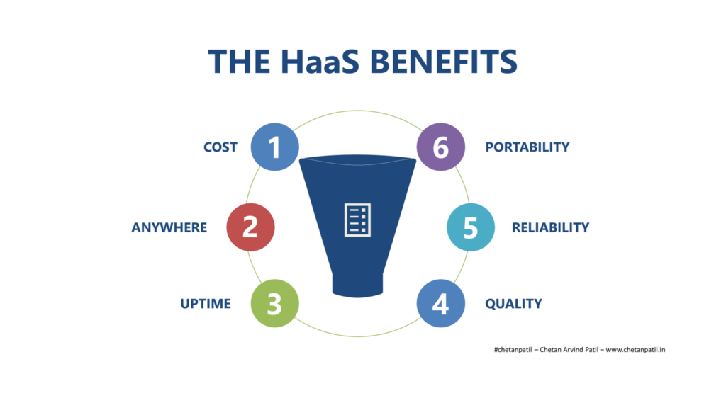
THE HaaS BENEFITS
Technology when applied correctly, provides numerous benefits. SaaS showed many benefits to the software world. Same applies to the hardware world due to the HaaS implementation.
Cost is one of the major benefits of HaaS. The ability to rent out as many nodes for as many days required has provided new way for consumers to manage the cost. In many cases, consumers can spend money wisely in other critical areas. The ability to terminate and forget about the infrastructure is also one keys to why the HaaS model is getting popular.
The HaaS provides a way to access services anywhere. From data centers to mobility all are available at the click of the button. The HaaS will be deployed and available at the doorsteps. Majority of the cities around the world are already equipped with several HaaS services and this has provided reliable uptime to the services.
Portability is another important benefit of HaaS. The option to switch smart devices to a new one without worrying about the cost is one example. Even with data centers, one can move from one cloud HaaS provide to another, without the need to understand the underlying process and technical challenges.
With SaaS, the quality and reliability of software services improved. Always on services and customer support was a great addition to the SaaS model and it has ensured that the customers are never out of help. The same quality and reliability solutions have been extended to the HaaS model and are taking the customer experience to a new level.
Digital transformation, expanding high-speed network, and advancement in the semiconductor solution is only going to improve the HaaS experience.
THE HaaS FUTURE
Given the expansion of the artificial intelligence and autonomous solutions, it is highly unlikely that the HaaS delivery model will change much from the existing one.
The HaaS in the future will keep evolving around the following three important aspects:
Users are the consumers for the HaaS model and paying for the service. Middleware is the connectors between the users and service providers and gets the share of both sides of businesses. Services are the different solution providers with innovative services and products.
It will be interesting to see if the industry moves to a new way of subscribing to the services. Currently, the business is moving around pay as a use model, and it has worked wonders both for the service providers and the consumers. However, every model evolves, and with the rate at which the technology is advancing, it will be important to adapt the business model accordingly. What new way of supporting these services will come, only time will show.