Heterogeneous Integration (HI) has become one of the most focused topics in the last decade. From academia to industry, everyone is publishing and launching innovative solutions to scale transistors per area out of the die. HI is also one of the paths (that soon) all of the semiconductors companies will have to follow for high-impact and core systems like XPUs.
For every new technology, there are basic blocks that are required to ensure the new technology is adopted speedily. The list of blocks can be endless and varies from technology to technology. The same is valid for new semiconductor technology, and the challenges become tenfold due to the time, cost, and resources required to make an idea work error-free.
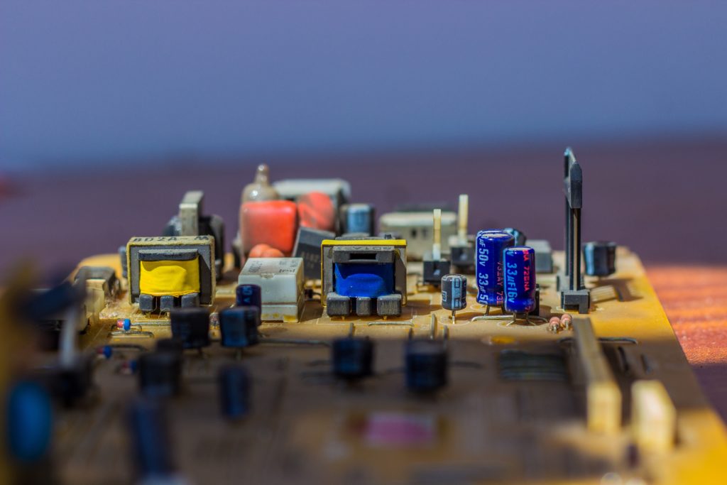
HI also requires several new and old building blocks to come together. Few of these blocks have been in use for decades (in the semiconductor industry), can be directly applied to HI. On another side, some blocks must get adopted for the HI.
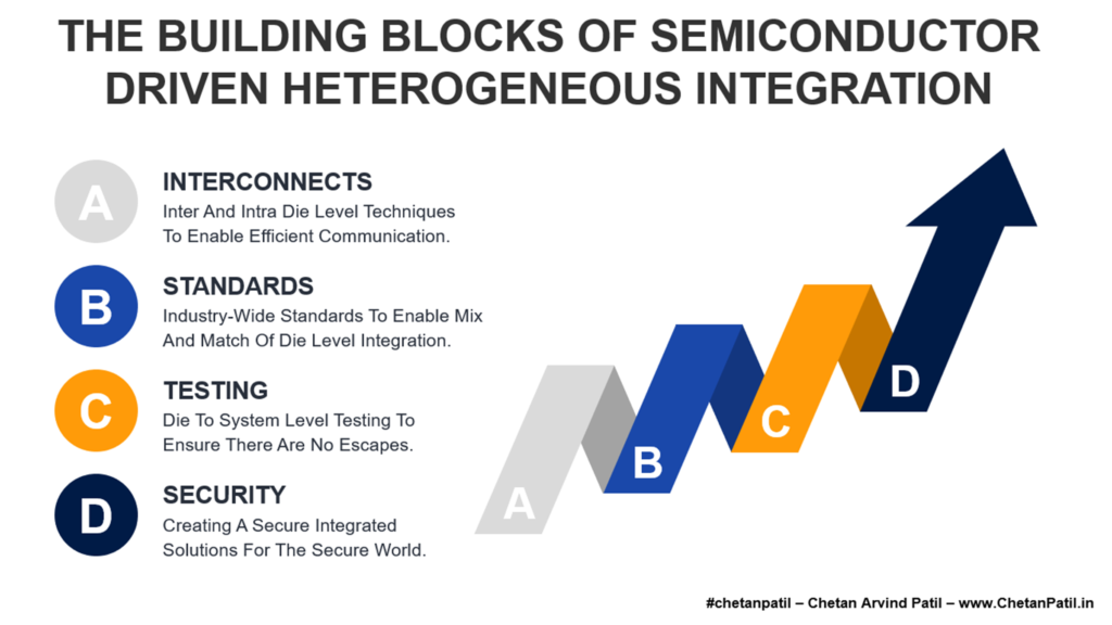
A couple of examples of such blocks are interconnected and standards.
Interconnects: Interconnects are vital in driving the data transfer rate, and that too without adding any bottlenecks. For HI, electrical interconnects can introduce bottlenecks and thus demand new solutions. Optical and Optical-Electrical are two approaches that HI systems are increasingly adopting to solve bottlenecks. In HI, die-to-die interconnect also becomes crucial apart from silicon/die-only interconnect. A perfect combination of die-level and die-to-die interconnect is vital for HI solutions.
Standards:In HI, the die can come from a different vendor (due to IP) or the same vendor. However, to drive efficient integration, die-to-die level standardization is required. One such example of standards is Advanced Interface Bus (AIB). As more companies come up with HI solutions, it will be crucial for all to come together and move forward with HI-focused industry standards.
Apart from interconnects and standards, the other two critical building blocks vital for HI: testing and security. In the end, to make a HI solution defect-free, the building blocks required will evolve, but it is good to make a few blocks of HI robust. Importantly, to increase the adoption rate.
Testing and security are other major building blocks of the HI world. These two together ensure the end HI-inspired semiconductor product meets the strict requirement of the industry. Without proper testing, there can be escapes that can lead to failures in the field, and similarly, without security, the product can be compromised.
Testing: Testing ensures all the parts and sub-blocks within a die work as expected. For HI, this process changes a bit as the testing now needs to occur at a multi-die level. The testing world will still follow the individual die-to-die testing plan, but it is equally vital to ensure the multi-die (something like chiplets) work as it should. It certainly requires new methods, equipment, and skills.
Security: Like monolithic chips, HI-driven chip development also demands secure solutions. During HI, it becomes more about ensuring no counterfeiting, which may occur with multiple moving parts. Thus, it requires a secure supply chain for a secured HI world.
HI provides a long-term incentive for the semiconductor industry by ensuring the next-gen solutions will not be defined by the technology-node. Instead, chip development will get ranked based on how they leverage different die level techniques to bring an integrated way to design and fabricate future chips.
One of the challenges for the HI solutions is the cost and time to manufacture. Taking the die level solutions and manufacturing it into multiple dies and then integrating is costly and requires capacity, and both are very difficult to balance.
Irrespective of where the semiconductor industry heads, the chip development process will become more HI, and it will open up new opportunities for the semiconductor design and manufacturing world.
The computer architecture design to cater the personal computing to data center needs has seen many changes over the last four decades. Computer architects have pushed the boundaries of designing novel ways to process data, which has lead to the manufacturing of advanced processing units (XPU) that are powering low to high-performance computing systems.
The growth of XPU is not only driven by the novel designs but also due to the shrinking transistor size. The advanced technology-node has allowed computer architects to take advantage of billions of transistors in the smaller area possible. With the ability to pack more transistors, the processing speed has increased, which has reduced the time taken to process user requests. All these hardware features combined with an elegant software system is powering the system to drive a rich user experience.
However, packing more transistors in the same area is hitting the wall. The benefits that Moore’s law provided a decade ago will not be applicable ten years down the line. Packing more transistors is not only leading to area-wall but is also adding power-wall, performance-wall, and thermal-wall. As more users come online, the expectation to provide real-time data processing will grow and this demands a new design and manufacturing approach for the next-gen XPU. The next-gen innovation should not only drive the required market growth and but must also ensure that the semiconductor industry never hits the usage-wall.
Heterogeneous Integration Is For Next-Gen XPU
On top of all this, the transistor size can not keep decreasing forever. The new technology-node also demands massive investment in the existing and new semiconductor fabrication facilities, thus pushing the semiconductor industry towards new XPU designs that uses a novel combination of technology-node and packaging solutions. These new types of CPUs are/will use heterogeneous integration for semiconductor designing and manufacturing.
There are two aspects of heterogeneous integration that any new emerging solution will have to consider before heterogeneous integration can be used to fabricate the next-gen XPU:
Design: Developing XPU with a heterogeneous integration approach needs different dies (sub-systems) to work in harmony. This demands cycle/time accurate communication between dies/blocks that may or may not come out of the same design team/company. To ensure all the dis-integrated systems can work in an integrated manner, requires a detailed design, verification, and testing approach. Without ensuring all the systems within the heterogeneous integration powered XPU working in synchronization, the end-product might not meet the expectation of the end-customers.
Manufacturing: Fabricating, packaging, and testing all the components of an XPU on a single die is a proven method. With heterogeneous integration, the dies (fabricated individually) will get integrated to form a single system. This will require a novel approach that is cost-effective and does not add a new bottleneck from a manufacturing point of view.
Heterogeneous integration and solutions around it are not new but will be when the industry moves towards large-scale adoption to design chips that follow the heterogeneous integration approach. The main reason is the bottlenecks and issues semiconductor companies without prior heterogeneous integration experience will face when they decide to venture into this territory.
Design and manufacturing are the two key areas that the emerging heterogeneous inspired XPU will have to focus on. However, there are several other challenges that both the existing and emerging solutions around heterogeneous integration will face.
Heterogeneous integration is touted as one of the More-Than-Moore solutions that can take away the need of shrinking transistor size further. However, there are few challenges to overcome when the XPUs are designed using a heterogeneous integration approach:
Data: The goal of any XPU is to ensure the data being processed flows across the blocks in the fastest possible time with near-zero latency. If the systems are going to be more heterogeneous and are stacked in such a way that they eventually have to communicate via a bus, then this may very well add data flow bottlenecks. This challenge can be overcomes via an optical interconnect system, but such solutions are not fully tested for a large-scale computing usage.
Power: Heterogeneous integration certainly provides avenues to overcome the challenges shrinking transistor size brings. However, the focus should also be on Performance-Per-Watt (PPW) to justify XPU designs that uses a heterogeneous integration approach. In the end, the goal of any processing unit like XPU is to provide maximum benefits at the lowest cost possible. Given, the demand to run more sophisticated graphics driven applications, the need to provide better PPW should be the priority of any heterogeneously integrated XPU.
Quality: XPU that will use heterogeneous integration will require qualification before production. In a monolithic chip, all the components are designed and fabricated together, which also gets qualified (JEDEC/AEC, etc.) for production use. However, with a heterogeneous approach, the singulated dies that form an integrated system will have to get qualified individually. This will increase the cost and time taken to execute the qualification plan, and might also raise the question on how different qualification criteria can be applied to integrated XPU.
Thermal: Controlling temperature ensures that there is no thermal runaway in any type of XPU. If heterogeneous integration will take the 3D approach, then managing die-to-die heat transfer can be a challenge. Fast heating will mean throttling the system often and will eventually impact the user experience.
Protocols: Heterogeneous integration also means integrating two different IPs. If the protocols to ensure smooth communication between these multiple dies are not defined and standardized across the industry, it might hinder the progress of next-gen XPU.
Packaging: Integrating all different die to eventually form a single system demands innovative packaging. While System-In-Package (SiP) based solutions are already out in the market, there is a need to test a different approach to packaging that ensures the area and thermal constraints are not leading to bottlenecks.
Above are few challenges that the next-gen XPU powered using heterogeneous integration may face. As more and more XPU design follow heterogeneous integration approach, the challenges can be overcome but might also lead to newer ones.
Above are the major challenges that the next-gen XPU powered using heterogeneous integration may face. However, there are several opportunities also that the heterogeneous integration provides.
The two major opportunities for the semiconductor industry if heterogeneous integration is adopted at a large scale:
Emerging Solutions: The solutions that heterogeneous integration can enable will be novel that can take the best of the IPs and integrate them to form an efficient computing system. These systems might very well provide high-performance computing to the general-purpose domain. The area to power wall can be overcome using heterogeneous integration and will drive design to packaging solutions. The only key is large scale usage as is the case with monolithic chips.
Cost Optimization: Yield is one of the major concerns when a single die is fabricated to manufacture XPU. With heterogeneous integration, there is a possibility to design and manufacture dies separately. It can bring down the wastage and improve yield, which in-turn will lower the cost and will certainly improve manufacturing efficiency.
The time of heterogeneous integration has come. Emerging solutions have started to embrace the possibilities heterogeneous integration provides. It will be interesting to see how general-purpose computing changes with heterogeneous integration design and manufacturing.
THE GROWING NEED FOR HETEROGENEITY IN SEMICONDUCTOR
The computing world today is all about processing data in real-time. Developers expect their code to compile in milliseconds. Consumers expect applications to respond with zero-delay. All of this requires a seamless communication of different computing components is a must, mainly the software (code) and the hardware (chip) is required.
The computing world pitched against the human brain. The ultimate goal is to outperform the human brain’s ability to sense, think, and act. While computers are outpacing humans, the desire for the silicon brain is still ongoing. To eventually mimic the human brain’s capabilities (mainly – sense, think, and act) demands much more computational speed and optimization than available today.
To reduce the time to run the compiled code on the chip has pushed both the software and the hardware (semiconductor) industry.
The software industry has been consistently coming up with unique ways to handle the data to avoid thrashing. Efficient use of parallel programming to split the single process/task into threads has been one major factor. Software developers (mainly frameworks and programming ones) have also been pro-actively utilizing all the hardware features (SVMS – Scalar, Vector, Matrix, Spatial) to enable a rich user experience by processing the data faster.
To Reduce Time To Completion While Balancing Performance-Per-Watt Is Pushing The Need For Heterogeneous SystemArchitecture
On another side, the hardware (semiconductor) industry is also innovating consistently (and trying to keep up with the software industry’s demand) to provide more performance-per-watt (PPW) that ensures the complex applications/workloads run efficiently. CPU/GPU/FPGA/ASIC design has seen not only architecture level innovations but also transistor-level. Shrinking transistor size made it possible to fabricate System-On-A-Chip (SoC) with billions/trillions of transistors in it. Transistor-level innovation has also allowed AI workloads to thrive. However, the SoC is hitting the design-wall and demands an innovative approach to cater to future workloads.
The SoC hitting the design-wall has pushed the semiconductor industry towards the Heterogeneous System Architecture (a.k.a. heterogeneous integration), which combines the best of the hardware capabilities to form a unique computing system. It allows the workloads to reduce time to completion while balancing the power-to-performance ratio.
Heterogeneous System Architecture requires unique semiconductor techniques that enable processing unit designs built using the best innovation out of the CPU, GPU, FPGA, and ASIC designs. It also drives the manufacturing process towards advanced technology nodes, packaging technology, and novel equipment.
THE SEMICONDUCTOR INNOVATION TO ENABLE HETEROGENEITY
Academia and the industry has been putting forward ways to design and manufacture architectures that can fit the demand for heterogeneous system architecture.
The heterogeneous system architecture can be classified into three categories:
Synchronous: Synchronous heterogeneous system architecture uses a single voltage, frequency, clock, and power domain for all of its processing units/cores. Multiple clusters with cores can exist, with each cluster designed using a unique data pipeline technique such that clusters are capable of operating at different speeds/frequencies. However, the processing units/cores within a cluster, always run under the same voltage to the power scheme. Apart from the CPU, the GPU (running on separate voltage to power domain) is the only other type of processing unit that is part of the synchronous heterogeneous architecture system. ARM big.LITTLE is one such example.
Asynchronous: Asynchronous heterogeneous system architecture borrows everything from the synchronous one, but it may also allow processing units/cores level voltage, frequency, clock, and power scaling. The helps in fusing cores/units on the same SoC that improves PPW. Qualcomm’s Snapdragon is one such example. However, the data pipeline of all the cores in the Snapdragon is the same. In reality, an asynchronous heterogeneous system architecture is not yet available as it demands innovative transistor-level techniques to drive per core level power domain apart from different core designs. There are thermal challenges too. Asynchronous heterogeneous system architecture often has another type of processing units/cores (FPGA, ASIC, GPU) apart from the CPU.
Fusion: In many architectures that form heterogeneous system architecture, per-core/unit level power management is not available. Instead, a fusion heterogeneous system architecture technique of combining different types (CPU, GPU, FPGA, ASIC, NPU, XPU, and so on) of processing units/cores are used. Each of these processing units may have separate power management. AMD’s Accelerated Processing Unit is an example of fusion without per processing unit/core power management. Fusion-based heterogeneous system architecture demand advanced technology nodes, packaging technology, and novel equipment
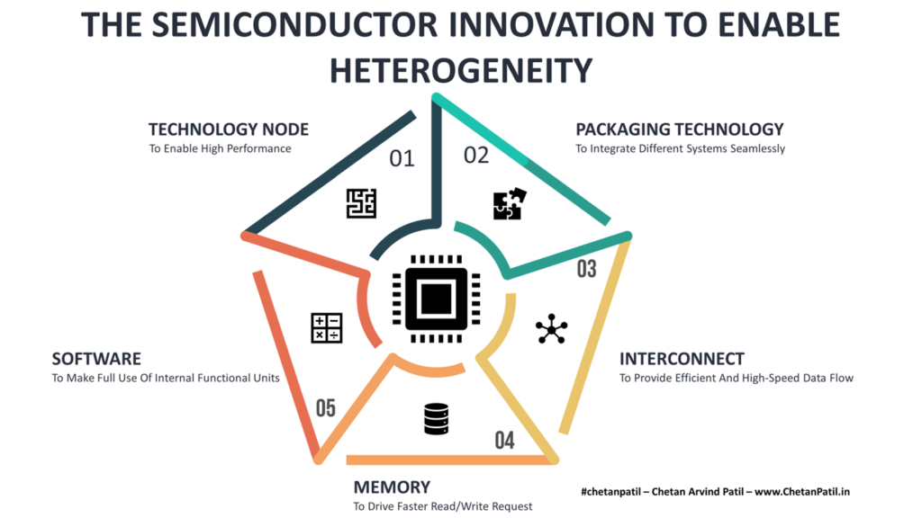
Whether one is designing synchronous or asynchronous or fusion heterogeneous system architecture, below are the five pillars of heterogeneous system architecture:
Technology Node: Integrating different processing cores/units to create a heterogeneous system architecture requires advanced technology nodes. The dies or the cores/units that get fused often have to get fabricated with the smallest possible transistor size. A true heterogeneous system architecture is supposed to make use of different technology nodes for the same integrated system. Example: A CPU inside a heterogeneous system architecture maybe 5nm, and the GPU might note be 5nm, and this pushes fabrication semiconductor companies to keep innovating on the transistor size and also on the device/transistor design/type (Planner FET, FinFET, GAAFET, MBCFET, etc.) Investing in Process Design Kit (PDK) and Electronic Design Automation (EDA) tools that can aid defect-free design is also required apart from developing fabrication facilities that can turn designs into silicon chips. All this puts pressure on the fabrication part of the semiconductor manufacturing process.
Interconnect: Faster data movement is key to enabling optimization on heterogeneous system architecture. Whether it is within the processing core/unit or in-between two or more, high-speed bandwidth is vital. Many are proposing silicon photonics-based interconnection that provides a high-speed interface. There are still open questions about the power requirements for silicon photonics-based solutions. It might be possible to make use of a photonics-based solution with electrical interconnects. Researchers have also proposed several solutions for heterogeneous silicon photonic interconnects. Eventually, continuous research and development is a must, as tomorrow’s heterogeneous system architecture will be highly complex than today’s.
Memory: Like the high-speed interconnect, high-bandwidth memory is also vital for heterogeneous integration to enable faster read/write for processing core-to-core (unit-to-unit). It may also act as a memory side cache. Intel’s MCDRAM is one such example. AMD also has hUMA that provides Heterogeneous Uniform Memory Access (hUMA) for fusion-based heterogeneous system architecture. Recently, Micron launched 176-Layer NAND, which delivers high performance and density. Similar techniques are required to enable faster input/output in heterogeneous system architecture.
Software: Efficiently scheduling tasks on a heterogeneous platform needs APIs, as it allows developers to map software on the target heterogeneous system architecture efficiently that allows access to internal functional units and drivers. Intel’s oneAPI provides exactly such an interface for its heterogeneous platform. Another approach is utilizing the Heterogeneous System Architecture Intermediate Language (HSAIL) which acts as an ISA for parallel compute routines. Software developers need to also make use of all the internal hardware features to drive the fastest time to completion.
Irrespective of the type of heterogeneous system architecture used – synchronous, asynchronous, or fusion – the above five components are crucial to take full advantage of the heterogeneous system architecture and its capabilities.
THE IMPACT OF HETEROGENEOUS SYSTEM ARCHITECTURE AND INTEGRATION
The impact of deploying heterogeneous system architecture is largely on the semiconductor manufacturing process due to the highly complex nature of fabrication, testing, and assembling the different types of sub-units using heterogeneous integration technology.
FAB: Semiconductor FABs have to always keep innovating new types of transistor devices, interconnects (TSV Interposers, etc.), and most importantly the advanced technology nodes. The demand and pressure to produce zero-defect products while the transistor size decreases is a challenge in itself. FABs like TSMC and Samsung have already started work on 3nm well before large scale production of 5nm, which is a challenging task. Lower technology nodes will enable highly complex silicon that is most likely be part of the heterogeneous system architecture. Fabricating 7/5/3 nm and beyond not only requires massive investment (upward of $10+ Billion) but demands continuous research and development too in close collaboration with academia. Heterogeneous integration is a vital market and is pushing the FABs to get into the packaging domain. TSMC already has a TSMC-SoIC solution for heterogeneous chiplets integration. Soon Samsung and others follow the suit.
Heterogeneous System Architecture Is Pushing Semiconductor Manufacturing To Innovate
EQUIPMENT: The equipment required to not only enable accurate testing but also assembling (Chiplets, Multi-Chip Multi-Die Modules, and SiP) without compromising on the specification puts pressure on the suppliers. The majority of the OSATs providing heterogeneous solutions will have to either upgrade their infrastructure or invest in new facilities. It is directly pushing semiconductor equipment providers to come up with new solutions.
COST: Eventually, aligning FAB to OSAT to equipment for heterogeneous integration requires CapEx. The added cost to design, fabricate, test, and assemble will increase the cost of development. It might directly affect the cost of goods sold, and semiconductor companies will have to come up with new techniques for viable product development to breakeven.
YIELD: All of the above factors eventually impacts the yield. The more complex the product is, the difficult it is to keep the yield high. Maintaining a high yield becomes a challenge due to the new way to test the system. This challenge is due to the complex fabrication and assembly process brings due to the integrated approach. It also means investing in new test hardware, probe cards, and automated test machines to handle heterogeneous testing.
The heterogeneous system architecture is pushing the manufacturing and the design semiconductor industry to new possibilities. It will be crucial to see how both the FAB and OSAT innovate and work in close collaboration with EDA and FAB-LESS/IDM houses to drive the era of heterogeneous integration.