Category: MANUFACTURING

  • The BIG-5 Are Becoming Semiconductor Companies

    The BIG-5 Are Becoming Semiconductor Companies

    Photo by İsmail Enes Ayhan on Unsplash


    THE NEED TO PROCESS DATA

    Internet usage is growing. Every new user generates a new type of data. The technology companies are always eager to process and understand new consumer behavior. It requires continuous research and development of both the software and the hardware.

    Software development has advanced in the last two decades. It has kept pace with the need to understand and process data due to the development of software libraries and frameworks. The large amount of data that has generated post-2010 has helped the Deep Learning (DL), Machine Learning (ML), and Artificial Intelligence (AI) frameworks train networks, and that is now allowing new data to be processed faster and accurately.

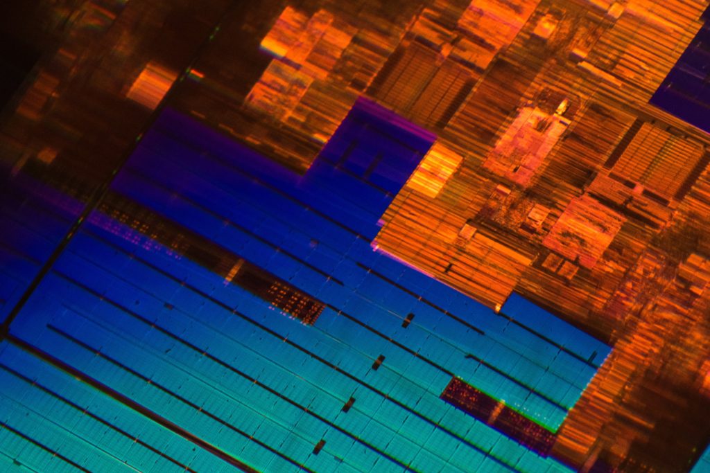
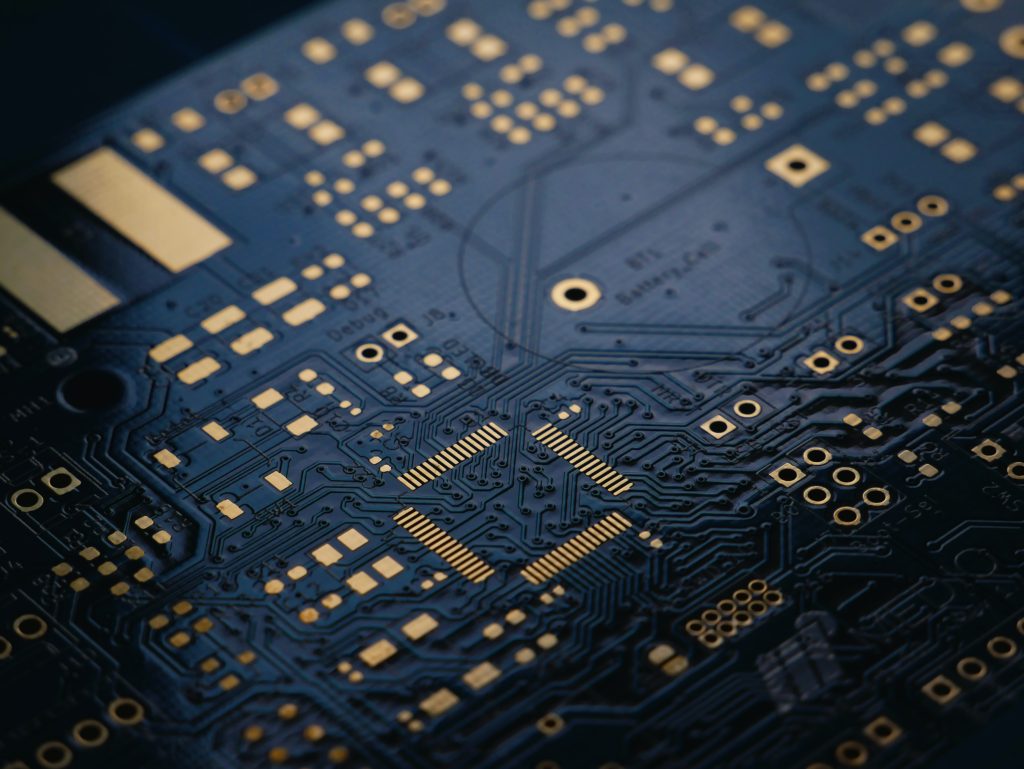
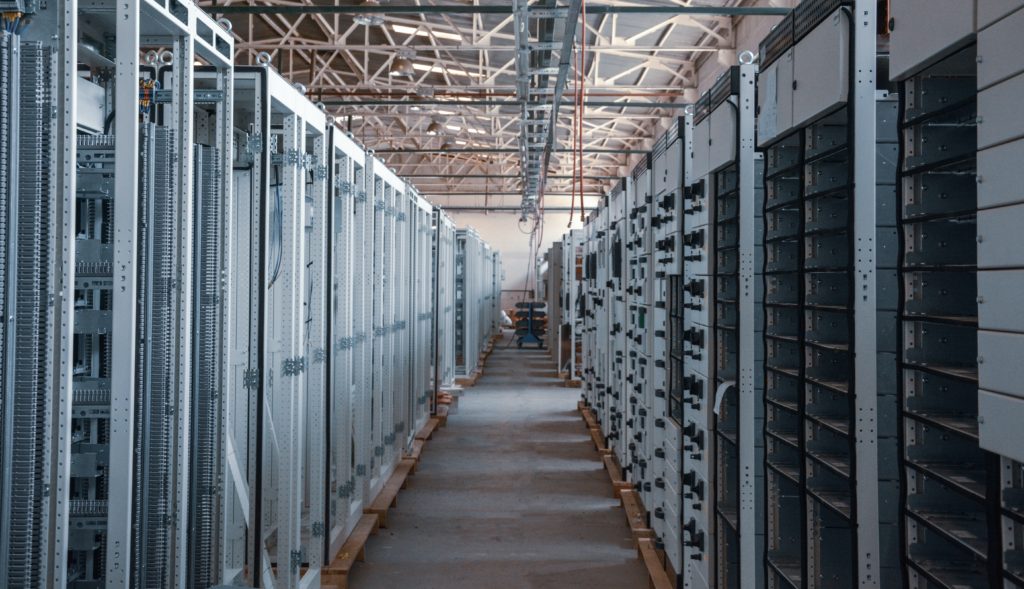
    Hardware is vital in ensuring that the processing of data using training and prediction frameworks occurs in the shortest time possible. It requires a massive amount of computing. The majority of the technology companies now rely on massive data centers equipped with advanced computer architectures.

    BIG-5Facebook, Amazon, Apple, Microsoft, GoogleFAAMG

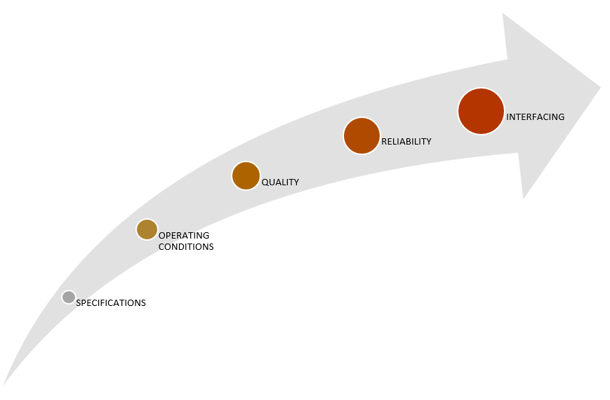
    To fully utilize computer architectures, an in-depth architecture-level understanding is required. It is not always possible to do so, as the data centers still run general-purpose computer architectures that do not cater to different types of data the big technology companies have to process.

    The disconnect between the software, the hardware, and the data has promoted the need to move from General-Purpose SoC To Application-Specific SoC. Not all data companies are capable of setting up a dedicated team that can focus on in-house silicon development to come up with an Application-Specific SoC.

    To overcome the reliance on semiconductor companies, the BIG-5 (FAAMG) technology companies have started (or have already developed) developing in-house SoC with the hope of opening up the silicon to different data companies around the world.


    Picture By Chetan Arvind Patil

    THE PUSH FOR IN-HOUSE SILICON

    Two major factors drive the push to develop new computer architectures (silicon):

    • Memory
    • Parallel computing

    Memory:

    • Modern applications are becoming memory intensive and also demand faster computation. To process requests from memory-intensive applications in the shortest possible time, the data needs to reside closer to the processing unit.
    • The time to bring the data from SSD to DRAM to Cache adds cycles and delays processing of the data. To overcome such bottleneck, semiconductor companies have implemented the following three techniques:
      • Cache Prefetching:
        • Bring the data near the processing unit in advance to minimize cycle time
      • Increasing Level Of Cache:
        • Add Leve-1 (L1), Level-2 (L2 – Shared), and Level-3 (L3 – Shared) small (KB/MB) cache memory to improve memory prefetching speed
      • Enable High Bandwidth Memory:
        • An extra layer of large high-speed memory between Last Level Cache (LLC – Either L2 or L3) and DRAM to speed up prefetching
    • All the above three techniques improved the response time of processing units. However, as the application data started growing, the cache and memory trashing became a new hurdle.
    • Multiple processing units sharing the same level of memory started corrupting each other’s data to process the request faster. On top of all this, the lack of interconnect bandwidth added further bottlenecks.

    Parallel Computing:

    • Apart from being memory intensive, applications have become compute-intensive too. It prompted the need to have multiple processing units within the same SoC. Running multiple data requests on a single processing unit or two separate processing units provided a way to accomplish the task in the shorted possible time.
    • The processing units still relied on the low-level memories to bring the data to be processed quickly. It means new SoC designing techniques that can allow the sharing of cache and high bandwidth memories in elegant ways without compromising on the need to add latency.
    • Adding more processing units to a single SoC is not the solution. On top, the developers have to keep comping up with smart ways to distribute the data to multiple SoC to speed up the processing.
    • Distributed computing is what the majority of the technology companies have adopted to ensure the data is processed quickly. It means a massive number of servers with thousands of SoC and a large amount of memory. Over time this has increased the cost of operating data centers.

    Even though in the last decade, semiconductor companies have come up with unique computer architecture to cater to both memory and compute-intensive applications, it has not been enough to adopt the changing processing requirement of BIG-5.

    The need to handle memory and parallel computing demand by modern workloads and applications efficiently at the architecture level has pushed BIG-5 to go for in-house silicon.


    THE STATUS OF IN-HOUSE SILICON

    BIG-5 has been gearing towards the development of adaptive computer architecture for data and operating systems.

    Facebook:

    Facebook started working on in-house silicon a couple of years back. With a growing user base across multiple platforms (Instagram, WhatsApp, Messenger), Facebook ramped up silicon effort last year.

    They have a silicon team that is focusing on Application-Specific SoC development that not only caters to data centers but also portable devices like Oculus.

    Amazon:

    Amazon Web Services (AWS) is one of the leaders in cloud solutions. The desire to have customized SoC is vital to ensure the consumers and enterprises can make most of the wide range of computing services AWS provides.

    Apart from AWS, Amazon’s growing range of Echo products is also pushing it to drive in-house silicon development. Amazon is betting big on ARM architecture to drive its silicon needs.

    Apple:

    Apple was always into silicon development. This year with the Apple M1 launch, they are making big bets on in-house silicon development that caters well to their need.

    With Siri about to become the default search option on all the Apple devices, the need to have data-centric customized silicon will grow.

    Microsoft:

    Microsoft always had a keen interest in hardware. They already have a strong team of researchers focusing on hardware research. The Surface line of products has shown strong growth, and the SQ1 line of SoC establishes Microsoft’s goal of making Windows smoother to use on silicon.

    Recently, Microsoft also announced a plan to develop Secure Chip with the help of semiconductor giant Intel and AMD.

    Google:

    Like Microsoft, Google also has a dedicated team that has heavily contributed to silicon development via different computer architecture domains. They have already announced plans to develop in-house silicon for Pixel and Chromebook devices.

    A few years ago, Google showcased the world Tensor Processing Units (TPUs) to speed up the training of data set using the TensorFlow framework. Google’s latest data shows they have been successful in doing so.


    Picture By Chetan Arvind Patil

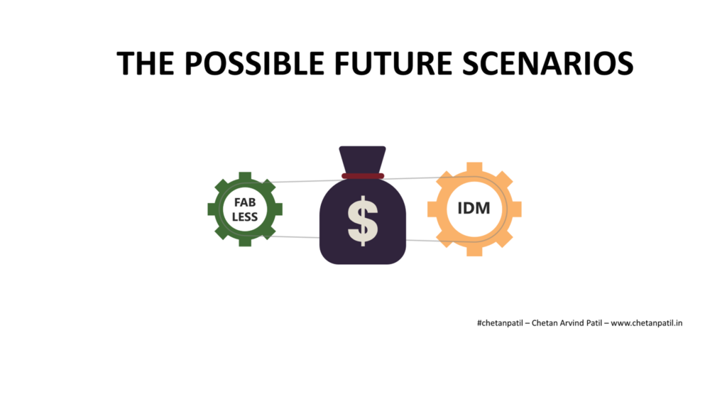
    THE POSSIBLE FUTURE SCENARIOS

    BIG-5 is betting big on in-house silicon development. This requires not only years of planning and investments but also a dedicated semiconductor development team and flow chain. Going forward there are two possible scenarios that BIG-5 might take:

    Scenario 1:

    BIG-5 will keep collaborating with semiconductor companies (Intel, ARM, AMD, and Qualcomm) to design silicon for their products and data centers with strict control over features and the manufacturing process. It will enable BIG-5 to enter the in-house FAB-LESS business model.

    Scenario 2:

    BIG-5 will slowly move away from semiconductor companies and spin-off an in-house team with a full turnkey silicon development chain. It will be more like an IDM business model and might require the acquisition of existing semiconductor manufacturing units.

    The probability of the second scenario occurring soon is unlikely. In a decade or so, BIG-5 may go big on the semiconductor business and try to keep themselves as in-house FAB-LESS silicon developers (while owning a piece of IDMs/FABs), which will ultimately play in the hands of FAB/Pure-Play Foundries like TSMC and GLOBALFOUNDRIES.

    Whichever scenario ends up occurring, there will be exciting developments in computer architectures that will drive the semiconductor industry to new levels.


  • The Semiconductor Industry Shake Up

    The Semiconductor Industry Shake Up

    Photo by Jason Leung on Unsplash


    THE SEMICONDUCTOR INDUSTRY STATUS

    In 2020, the semiconductor industry has seen both negative and positive trends.

    The first half of 2020 showed mostly the negative trend driven by the COVID-19 restrictions, as it lead to slower semiconductor production and increased inventory due to decreasing salesThe second half of 2020 has been more positive. The sales have gone up and production lines are 100% occupied, to cater the newly launched devices and products by vendors across the globe.

    Apart from the steady increase in design, development, and production, merger/acquisition have gone up too. There have been some unexpected takeovers which are bound to have a strong impact in the long run.

    The semiconductor industry from a product point of view can be divided into:

    • CPU
    • GPU
    • SoC/MPSoC/RFSoC
    • ASIC/FPGA/ASSP/ACAP
    • Digital/Analog/Mixed
    • Memory
    Picture By Chetan Arvind Patil

    The mergers and acquisitions that have occurred in 2020 have affected each of the above product domains.

    All these acquisitions from the design have shaken up the semiconductor design industry. However, at the same time, it is turning out to be a boon for semiconductor manufacturing, as many IDMs plan on becoming FAB-LITE to focus more on the design aspect and increase share the mobile, AI, and data center market.

    This raises the question of how the future of semiconductor design and manufacturing is going to be.


    THE SEMICONDUCTOR INDUSTRY SHAKE UP AND FUTURE

    Taking a look from the semiconductor design point of view, it is getting clear that companies are more focused on a specific product domain and want to dominate the market. To achieve this, companies are either creating new asset via acquisition or selling old asset that do not align with the goal.

    Intel last year sold its smartphone modem business to Apple and this year Intel also decided to sell NAND memory business. This shows that Intel wants to focus on its strength of personal and data center computing. For sure, NVIDIA’s acquisition of ARM is concerning for Intel, given how much strength an established IP from ARM will give NVIDIA and also allow it to extend its business from GPUs to CPUs, and that too smartphone business which is not Intel’s primary domain.

    On top, with AMD’s solid performance and acquisitions, the fight for smart computing is going to heat up. AMD (since 2009) and NVIDIA are FAB-LESS semiconductor companies. This allows AMD and NVIDIA to focus more on the design aspect and let external manufacturers take care of the manufacturing. This is a big advantage as semiconductor manufacturing is hard and takes a long time to perfect.

    Picture By Chetan Arvind Patil

    All these points towards a major shake-up that will occur in near future. The business mode; will change and semiconductor companies will go either:

    • FAB-LESS
    • FAB/Pure-Play Foundry

    Competing in both the arena as a single entity is going to be challenging. Spinning off or selling part of the semiconductor manufacturing might be a more viable solution. Such shake-up will eventually end up creating more business for the semiconductor manufacturing companies and they will have to predict today and start planning on increasing the capacity (or acquisition) to keep the business running.

    It will be vital for countries like India to take advantage of such market business change by coming out with policies that heavily incentivize semiconductor manufacturing.


  • The Data-Driven Approach Towards Semiconductor Manufacturing

    The Data-Driven Approach Towards Semiconductor Manufacturing

    Photo by Vishnu Mohanan on Unsplash


    THE GROWTH OF DATA IN THE SEMICONDUCTOR MANUFACTURING

    The growth of digitization has led to the generation of massive amounts of data on day to day basis. The data explosion has pushed several industries to adapt to data-driven analysis and decision-making processes. The same is true for the semiconductor industry.

    Data was always an integral part of semiconductor design and manufacturing. The need for data has increased further due to the cost and risk involved in designing products that are becoming smaller and smarter. The cost to fabricate semiconductor products is high and that is why during the design phases innovative simulations/modeling approaches are used to validate product design against specification before sending the final design files to the semiconductor fabrication houses. The risk of not spending time to collect and review semiconductor data both during the design and the manufacturing stage can cost a lot of money and time if the product starts failing in the field. 

    Data-Driven Approach Is Raising The Bar Of Semiconductor Manufacturing

    As the technology-node and package technology have advanced, so needs to take a data-driven approach to semiconductor manufacturing. The goal of the data-driven approach is to ensure that the products being are defect-free. The sophisticated tools and equipment used by the semiconductor manufacturing process have only gotten more advanced. The de-facto feature of these system-driven tools is to capture data and present it in a form that makes the decision-making process easier and faster.

    The data-driven approach is required to meet the following two important requirements of semiconductor manufacturing:

    Quality: Qualifying every semiconductor products is vital. It has to meet different industrial standards. Automotive semiconductor products have to go through one of the most stringent qualifying processes to ensure the product can work seamlessly everywhere. It is vital to ensure the manufacturing process established meets the high standards of quality requirement, which is possible only if the data captured to drive the decision-making process.

    Waste: Every data point tells a story. In semiconductor manufacturing, data can be about the design or the manufacturing tools, or handling issues, and many more. Every semiconductor data type counts towards ensuring the wafers and assembled parts are not getting scrapped. Scrapping raises yield concerns and indirectly impacts the cost.

    Without investing time and money in the data-driven approach to manufacturing semiconductor products, the semiconductor companies run into the risk of overlooking the quality metric. Driven by the need to ensure the products using the semiconductor solutions meet user satisfaction, the customers/companies using the semiconductor products are increasingly using Defective Parts Per Billion (DPPB) as a new metric than Defective Parts Per Million (DPPM).

    The need to capture, process and review semiconductor manufacturing data is becoming vital when there is a possibility that the semiconductor device might end up powering critical infrastructures likes satellites to aerospace to automotive (and many other solutions).

    All this is why the semiconductor industry is becoming more data-driven than ever before. The manufacturing part of the semiconductor process is not complete without letting the data speak.


    Picture By Chetan Arvind Patil

    THE PROCESS TO CAPTURE DATA IN THE SEMICONDUCTOR MANUFACTURING

    The semiconductor manufacturing process is a well-established flow. While every product has different requirements driven by the specification it is supposed to work within, some standard flows/stages are common across numerous semiconductor products.

    These processes use tools/solutions/recipes to capture data, which eventually drives a data-driven decision-making approach in semiconductor manufacturing.

    Following are the major process that leads to capturing of semiconductor manufacturing data:

    Fabrication: The first step towards semiconductor manufacturing is to fabricate the product on the wafer. Every layer/mask/stage of the semiconductor device fabrication is data-driven. If the data does not align at the etch or the lithography stage (for example), the wafer/lot cannot move forward. Several modules are placed in the kerf region of the wafer to data of the devices (that eventually make up the full die) to ensure is no deviation in the semiconductor wafer. All this data is unique to the technology-node. At the end of the wafer fabrication, data in the form of visual images ensure no particles or scratches are present on the wafer/die.

    Wafer Test: The defect-free wafer coming from the semiconductor fabrication facility gets sent to the test facility. The wafer test stage ensures all the die on the wafer gets electrically tested with the test program to validate whether the die meets the specification or not. The good and the bad die are marked accordingly. All this is possible due to ATE tools and probing hardware. The data is analyzed to understand any excursion, which eventually gets debugged to ensure no test escapes. 

    Final Test: The final test can be performed on the wafer (Wafer-Level Chip Scale Package (WLCSP)) or on the assembled parts (non-WLCSP). The final test uses similar testing criteria and tools like the wafer test). The major difference is the packaging testing versus dies testing. The data points are specific to the package testing. This is often the last electrical data point the semiconductor manufacturing process generates before the parts are shipped to the end customer or assembly.

    Assembly Inspection: Post assembly, the visual inspection of the assembled parts is carried out. The tools used for visual inspection capture all sides of the assembled parts. The data in the form of images show if chipping/defects occurred during the assembly process. If so, then the root cause needs to be determined. The data in the form of images often requires a highly automated system to alert any defects.

    System Testing: A final system (like a smartphone) not only uses one specific semiconductor product but several others. All the different semiconductor products are assembled onto the Printed Circuit Board (PCB) and should work in harmony. If anything fails, then the data relevant to the failing semiconductor product is capture and sent to the company that fabricated it. System testing also drives the semiconductor manufacturing process from the customer side.

    Miscellaneous: The last data point in the semiconductor manufacturing are from the equipment that enables the different process. These need periodic maintenance to avoid breakdown. All the equipment connected via a Manufacturing Execution System (MES) is monitored to capture every activity the equipment/tools perform. This data is vital for keeping the semiconductor manufacturing facility up 24x7x365.

    The above data points are vital in ensuring the semiconductor manufacturing process is fabricating/testing the high-quality products that meet the stringent quality requirements. To ensure, the high-quality demand data-driven process is critical in semiconductor manufacturing.


    Picture By Chetan Arvind Patil

    THE ADVANCED DATA APPROACH IN THE SEMICONDUCTOR MANUFACTURING

    Even though data exploration in semiconductor manufacturing is not new, the need to take a different data analysis approach is growing. The main reason is due to the high cost required to generate the semiconductor data. In the smallest data available, the semiconductor engineers need to predict that the products will work in the market as per the specification.

    To lower the time taken to move the wafers to the next stage, the semiconductor manufacturing process is relying on different advanced approaches to enable data-driven semiconductor manufacturing:

    Algorithm: Due to the proliferation of fast systems that can crunch data on the go has led to the development of algorithmic solutions that can detect scratches, clusters, excursions, particles, etc., faster than ever. The algorithms deployed can capture the patterns to raise an alert if there are issues with the semiconductor manufacturing process. These algorithms take the help of numerical data or visual data. Visual data is more vital as it shows gate-level details using an advanced microscope. There are already solutions, but there is a need to minimize the time taken for decision making as spending more time to decide on the correctness of the product means holding the lot/wafer from releasing, which can be costly.

    Analytic: Data lying without insights is not useful. Given that every die/chip that gets shipped out of the semiconductor manufacturing flow is visualize/tested, it is important to develop an analytical approach that uses computational analysis of statistics to drive data exploration. It helps the semiconductor data engineers to visualize data using diverse statistical methods to find issues/outliers. Analytical solutions are already available in the market/industry, but often requires skills to look beyond what is being presented on the dashboard.

    Tool: Tools are required to view the detailed history of every die that gets manufactured. The standard process to capture and store is already defined. The end-to-end semiconductor manufacturing data analysis still requires different tools to visualize and critically analyze the data. One single data tool may not be enough. It is good to test and use data analytical tools (or programming methodologies) as per the need to drive the decision-making process.

    Decision: Eventually, the goal of data analysis in semiconductor manufacturing is to either hold or release the product. It requires the perfect combination of computer and human. Computers can enable data collection and storage. However, the data wrangling is still on humans. In semiconductor manufacturing, every new data requires a new inspection approach as every new product is different from the last one. All this means every changing data-driven approach to decision-making (hold or release).

    The speed at which the semiconductor industry is driving towards the shirking technology-node year-on-year, the process to scrutinize the data will also change, and the semiconductor data inspection process will keep getting directed towards new ways to enable the smarter data-driven approach towards the semiconductor manufacturing.


  • Data Enabled End-To-End Manufacturing

    Data Enabled End-To-End Manufacturing

    Photo by Laurel and Michael Evans on Unsplash

    Industry 1.0 was all about the transfer of manufacturing from humans to machines. Industry 2.0 increased productivity by using technology-enabled information and faster transfer of goods. With Industry 3.0, computers took over machines and allowed efficient manufacturing compared to Industry 2.0.

    Today, we are in Industry 4.0. This is all about data gathering at each stage of end-to-end manufacturing to allow the right product at the right place at the right time with minimal waste and downtime.

    In order to fully achieve Industry 4.0, there is a need to understand how efficiency can be achieved, and to do so one has to look at each stage from a data point of view. Without capturing data information at every stage of manufacturing, it is difficult to remove bottlenecks.

    Photo By Chetan Arvind Patil

    PROCUREMENT

    Procurement is the defacto process for any manufacturing domain. Does not matter what type of products are being developed, manufacturers have to keep track of inventory.

    During the pre-computer era, this process required manual bookkeeping and then actions would need to be taken based on when raw materials are going to be out of stock. This meant the raw materials were ordered without understanding whether the market demand, thus leading to waste of manufactured goods and money.

    In the post-computer era, this process moved from books to computers. Software was deployed that could keep track and alert beforehand. However, this process was still similar to the pre-computer era, except that humans could do be used for more productive work than bookkeeping.

    Photo By Chetan Arvind Patil

    In today’s day and age, the need is to make procurement more real-time, smart and market demand-driven. Toyota Production System follows the concept of Just-In-Time (JIT) manufacturing since the 1970s. It is more relevant today where cost saving is critical while ensuring market demand is met. In order to achieve efficient manufacturing, data from different vendors need to be connected in real-time. This allows the end customer to understand how late OR how early they should procure the raw material based on the demand of the product.

    Enterprise Resource Planning tools are increasingly being used to provide such solutions. However, they cost a fortune to deploy and manage. Dedicated teams are required. A big enterprise might find it easy to make use of such tools, but small manufacturers will financially struggle to get such a system deployed.

    With the advancement in connectivity and computing if such gaps can be filled while ensuring minimum impact on the expense, then procurement (the stepping stone of manufacturing) can be made more efficient by tapping into the data information.

    MANUFACTURING

    After procurement, comes the real task of manufacturing. When goods are being manufactured the focus is on cost efficiency by achieving maximum uptime with minimum downtime. We are living in an always-on world, where things need to keep running 24×7 to achieve more profits year on year. The same applies to machines that are churning out goods. Here too, does not matter what domain is being catered; machines and tools need to be up and running all the time. An idle machine in manufacturing is a liability.

    In order to achieve 100% uptime, a critical factor is to predict downtime. Predictive downtime requires capturing real-time data. Data can be about how old the parts are, have parts are aging based on usage, when should parts be replaced and serviced, when should machine go through calibration, is demand going to keep machine idle, how can resources be planned efficiently and many other data points.

    Photo By Chetan Arvind Patil

    Oil and gas production has to be up and running 100% of the time. To achieve 100% uptime, the oil and gas industry has taken an advanced approach and adapted to data-enabled production. Manufacturing in today’s date is not just about production engineering, it has to have a data engineering aspect where data is captured, stored, analyzed, and presented for pro-active action.

    Capturing all such data points and presenting in a single dashboard can provide much more insight into the manufacture than waiting for the machine to go down. All of this requires a drastic change in the way of working so that resource planning for manufacturing is made more data-driven. Data-enabled manufacturing solutions are already present and it is time many manufacturers start taking data aspect into production to achieve 100% uptime.

    TESTING

    Testing is the most critical process during manufacturing. Now only the product should meet all the requirements under quality, reliability, and operating conditions, the data generated during the testing process should also be analyzed thoroughly and stored in case of any customer return.

    Photo By Chetan Arvind Patil

    The last thing the manufacture wants is another Samsung Galaxy Note 7 situation where the smartphone exploded due to faults in the battery. Depending on the product the test data can be captured using different tools and processes. This requires implementing a software interface that can log the data during the testing process. Then, based on the specifications applicable, it can be then put through different operating conditionsquality, and reliability checks before putting through interface testing for a real-world application.

    Today, there are different analytical tools that are available in the market that are proving to be critical for productivity and probability. Data generation, data analysis, data action, and data storage in itself going to be a trillion-dollar industry. The solutions provided for manufacturing analytics with respect to testing are many. It is critical for product development and manufacturing companies to embrace and find ways to implement data-driven testing within the manufacturing cycle.

    After all the testing and quality requirements have been met the product can move to the next stage of manufacturing.

    PACKAGING

    In the US alone, 165 Billion packages are shipped every year and this is just e-commerce data. 50% of these packages end up being waste and not getting recycled. This clearly points to the need to make packaging more efficient.

    LimeLoop and Repack provide solutions to enable re-use of packaging. However, this requires tracking of where the package is being used and then need to re-ship the empty packages. This is not a practical solution for a custom manufacturer dealing directly with businesses that are not into e-commerce like car manufacturers, electronic design and manufacturing, and many other domains.

    In order to achieve efficiency in packaging, manufacturers need to follow data enabled packaging by considering following points:

    • Quality
    • Waste
    • Usage
    Photo By Chetan Arvind Patil

    Quality enables whether the product being manufactured and being shipped in certain packaging meets the required industry standards. This means tracking the data points of happenings with respect to packaging. The old-age process of using cardboards to package is only going to add cost and eventually leads to waste. To understand where cost savings can be achieved, it is critical to capture data points on the usage of the package. All this eventually allows innovation within the packaging domain to make more informed decisions.

    For example: Is there a way to package products in small form factors which can in turn save packaging cost including on shipping? This cannot be achieved by package innovation, which requires data capturing of the packaging within the manufacturing unit.

    LOGISTICS

    Out of all the blocks of manufacturing, logistics is the most advanced and has embraced data faster than any other sector. It has been the leader in data usage and driving it for the efficient delivery of goods.

    For manufacturer data usage in logistics means tracking the market for the least expensive way to ship the goods from point A to point B. Traditionally, big manufacturers try to save cost by means of entering contracts with giants like UPS, FedEx and DHL, which will provide cheaper cost for a certain number of shipments for the agreed period. However, smaller or mid-scale manufacturers do not have this luxury.

    Thanks to data sharing there are more than ever data points on the way to ship goods from one place to another and also understand a cheaper way to ship the product to the end customer. There are already many companies that have started to provide data-driven logistics to small and medium scale industries.

    To save cost, the planning team also needs to become more data-aware and then find ways to implement strategies to utilize cost effect logistics.

    Photo By Chetan Arvind Patil

    Currently, the majority of the manufacturer is shipping even before understanding market needs. That also means manufacturing before capturing demand. To save cost and be more efficient demand can be re-factored by implementing just in time stocking to save cost on shipping the product earlier than required.

    Logistics data analytics just does not apply to final goods, but to also to the raw materials. This is why the scope to save costs is much broader than one can imagine. It is time manufacturers embrace data tools to provide more insights to cost savings on logistics.

    DISTRIBUTION

    Distribution is more about after-sales handling when manufactured goods have shipped out. Data in the distribution has been more critical for e-commerce where manufacturers can directly engage with customers by eliminating distributors.

    In the age of data drove process and decision making, it is more critical to understand how data allows distributors to manage inventory and tap into the next era of the supply chain. For manufacturers, the less the number of stops from the factory to end customers, the more profits they can make. For distributors to be relevant, they need to keep track of industry demand and come up with a supply chain system that provides cost-saving and at the same time real-time delivery.

    Photo By Chetan Arvind Patil

    If the customer needs the parts as soon as possible for the critical task that is stopping the production, then it becomes all about who can provide the needed goods in the fastest way possible. For such scenarios, it is important to tap into the data points in terms of usage and manufacturing.

    • From customers, distributors need to understand ways to leverage real-time usage of the parts so that they can ship when required and in some cases beforehand considering the aging the raw material has wen through.
    • From the manufacturer’s side, they need to keep track of real manufacturing throughout. This has to be the balance of demand and supply without getting into waste.

    This requires the implementation and usage of data tools that can provide distributors more than just inventory stock. There are already solutions out in the market, it is just about investing and understanding how distribution make most of the data-driven manufacturing.


    INDUSTRY 5.0

    As manufacturer look to increase the EBITDA, industry 4.0 is going to be a big driver for it by leveraging data points at each step of the manufacturing.

    Photo By Chetan Arvind Patil

    In a few years, the industry will soon transition to Industry 5.0 which will be more about smart automation with respect to decision making. These smart decisions will be towards reducing waste, enabling efficient processes hopefully without impacting human resources, and delivering what the customer needs by adapting products to their requirement.

    It is going to be a combination of Data, Connectivity, Intelligence, and Automation. May be 3D Printers are the first step towards Industry 5.0.


    PSA

    McKinsey & Company has useful resources for those interested in learning more about data enabled manufacturing.

  • PCBWay – Smart PCB Prototyping And Manufacturing

    PCBWay – Smart PCB Prototyping And Manufacturing

    Photo by PCBWay

    Developing an electronic product requires a lot of iteration. A hardware electronic device has to go through a detailed design process which is followed by numerous prototyping and evaluation. It is often a time-consuming and cost-intensive process.

    Not all the development processes happen in the house. The majority of the companies do in house designing and then rely on trusted partners to manufacture prototypes and later on the scale based on the outcome. It is critical to understand how one can design and where one can manufacture.

    MAJOR STEPS IN HARDWARE DEVELOPMENT

    There are two major steps before the hardware product hits the market: Designing and Prototyping

    Designing a hardware product for consumers requires a dedicated team that can provide proof of concept using different tools. After the idea is validated using circuit simulation tools, then the team will generate a detailed Bill of Materials (BOM) which will have all the details regarding components required to assemble and manufacture a hardware prototype in form of Printed Circuit Board (PCB). In most cases, the designing team will also provide Gerber files that will have the details of how many layers the PCB will have, which components are placed at what locations, orientation of the components, and many other assembly related details. All these technical details and information is then sent to the team which is capable of producing PCB for rapid prototyping.

    Prototyping is a very complex process and requires that the BOM being assembled adheres to industry standards. Majority of the prototyping happens using PCB which is outsourced. To assemble PCB, the service provider should have dedicated tools and teams that can take Gerber files, validate that it is correctly designed, and then process it through the manufacturing flow to provide faster PCB prototyping.

    WHERE TO MANUFACTURE

    There is no denying that China is the leader in PCB assembly with over 50% of the global market share. Shenzhen, which is often termed as The Silicon Valley of Hardware, is the go-to place when it comes to prototyping and large scale manufacturing of hardware products.

    Numerous companies provide elegant solutions in China and PCBWay is one of the leading manufacturers of PCB designing, prototype, fabrication, and assembly. It is one-stop solution for all things hardware manufacturing.

    PCBWay has opted a different approach that combines the power of software and hardware to provides manufacturing without compromising quality while ensuring timely delivery and cost effectiveness

    It is becoming a powerhouse of smart PCB prototyping and manufacturing.

    THE PROCESS

    PCBWay makes sit very easy for any customer to get started with the service. Traditional there are two types of design and development companies:

    • One which prefer to only outsource PCB and then do assembly either in a house or at other vendors
    • Second which wants everything to do done the same manufacturer: PCB, assembly, testing and scaling
    Photo By PCBWay

    For both such types of companies, PCBWay has solutions. Using PCBWay’s online quotation system designing company can opt for a quick quote. Apart from standard single-layer PCB, the company offers advanced multi-layer PCB designing and prototyping. Flexible electronics is one of the upcoming markets and PCBWay already has technology that can easily provide rapid prototyping and assembly of flexible PCB.

    All this is very handy for customers who would like to just get a quick prototype of PCB built based on the design provided, and later on, prefer to assemble somewhere else.

    If the OEM wants everything from PCB designing, manufacturing, and assembly to be done at a single location, then PCBWay already has all such resources. They can handle sample prototyping to turnkey production.

    Photo By PCBWay

    QUALITY

    It is very critical to ensure that any hardware being assembled goes through all the required quality checks. PCBWay assembly and manufacturing adhere to all such requirement that includes design rule check, automated optical inspection, electronic and probe test, automated X-Ray inspection, impedance control, RoHs lead-free, UL certification and different manufacturing tolerance.

    They have also partnered with leading design houses which ensures all these quality requirements are met from day one.

    COMMUNITY

    Apart from catering to the industry, one of the major steps PCBWay has taken is to differentiate itself from other manufacturers in China by engaging with electronic enthusiasts. They often run an online competition and PCBWay Community is one of the fastest-growing assembly communities.

    Anyone with or without knowledge about PCB manufacturing and assembly can sign up and learn rapid prototyping.


    PSA

    If you watch videos from Scotty Allen then you will definitely like below one by him on PCBWay.