Category: METROLOGY

  • The Semiconductor Metrology

    Image Generated Using DALL-E


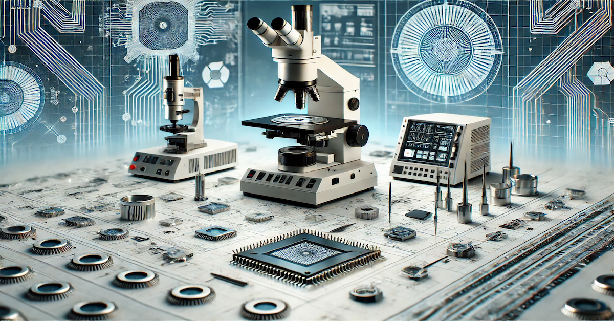
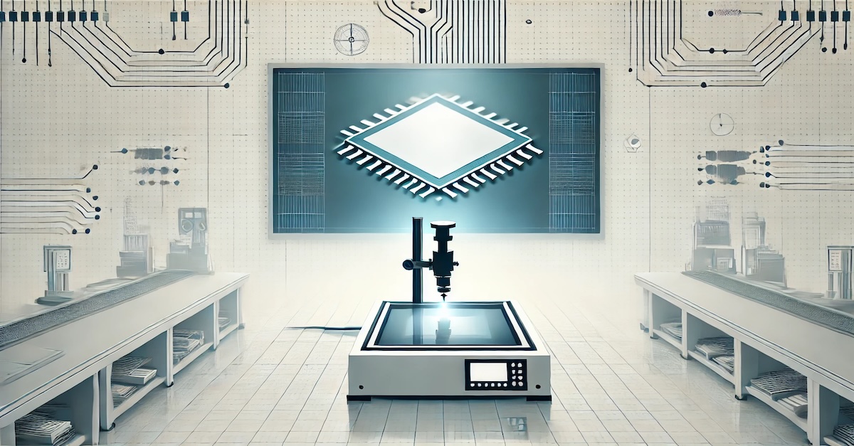
    What Is Semiconductor Metrology

    Semiconductor Metrology is the science and technology of measurement explicitly applied to semiconductor manufacturing processes. It encompasses the tools, techniques, and methodologies used to measure and analyze various aspects of semiconductor materials, components, and devices. The primary goal is to ensure that chips meet stringent design and performance specifications.

    Below are the key aspects of semiconductor metrology:

    Key AspectsDescription
    Dimensional MeasurementsPrecise measurements of nanoscale features, such as line widths, spaces, and pattern dimensions on wafers.
    Material CharacterizationAssessing the chemical composition, thickness, and uniformity of films and materials used in semiconductor fabrication.
    Defect DetectionIdentifying and analyzing defects on wafers or during the manufacturing process, critical for improving yield.
    Critical Dimension (CD) ControlMonitoring and ensuring that the dimensions of semiconductor features stay within allowable tolerances.
    Process Monitoring and ControlUsing metrology data to monitor process consistency and adjust manufacturing processes in real-time.
    Optical and Electron-Based TechniquesUtilizing advanced tools such as Scanning Electron Microscopy (SEM), Atomic Force Microscopy (AFM), and Spectroscopic Ellipsometry.

    Why Metrology Is Crucial For Semiconductor Manufacturing

    Metrology is crucial for semiconductor manufacturing, as it ensures dimensional accuracy by verifying nanoscale features meet strict design specifications, enabling advancements in technology nodes. It enhances yield by detecting and preventing defects early in the process, reducing waste, and improving production efficiency. It also enables precise process control, ensuring consistency and minimizing variations across wafers. This is vital for scaling to smaller nodes like 3nm and 2nm. It also improves reliability by ensuring devices meet performance standards, reducing field failures in final products.

    Additionally, it optimizes cost efficiency by identifying process inefficiencies and defects, minimizing rework, and accelerating innovation by providing critical data for developing new materials, processes, and devices. Apart from this, metrology in semiconductor manufacturing also supports advanced technologies like EUV lithography and 3D packaging, making it the backbone of precision and operational excellence in semiconductor manufacturing.

    What Are The Skills Required Based On Metrology Specific Career

    A career in semiconductor metrology requires a unique combination of technical knowledge, analytical skills, and adaptability. A strong foundation in physics, material science, and semiconductor manufacturing processes is critical. Professionals need to understand the properties of materials and how they interact with advanced tools such as Scanning Electron Microscopes (SEM) and Atomic Force Microscopes (AFM).

    Skill CategoryDetails
    Metrology ToolsExpertise in SEM, AFM, Ellipsometry, and Optical Profilometry.
    Semiconductor ProcessesKnowledge of lithography, etching, deposition, and Chemical Mechanical Planarization (CMP).
    Data AnalysisAbility to interpret statistical trends and patterns in measurement data.
    PrecisionAttention to detail for working with nanoscale measurements and ensuring high accuracy.

    Analytical and data skills are critical for semiconductor metrology professionals. Using statistical tools and techniques to identify trends and anomalies in measurement data is essential for ensuring process accuracy and reliability. Understanding basic machine learning algorithms also enables professionals to process large datasets effectively, derive actionable insights, and enhance process control. Familiarity with programming languages like Python, MATLAB, or R further supports data analysis and reporting automation, allowing for efficient interpretation of raw data and optimization of processes based on measurement trends.

    The Future Of Metrology In Semiconductor Manufacturing

    The future of semiconductor metrology is evolving rapidly to address the growing complexity of advanced technologies and smaller technology nodes. As the industry progresses to sub-2nm nodes and beyond, metrology will play a pivotal role in ensuring precision, yield, and efficiency. Emerging trends in artificial intelligence, non-destructive techniques, and advanced tools are set to redefine how measurements are conducted in semiconductor manufacturing.

    Here are the key developments shaping the future of metrology:

    Precision for Shrinking Nodes: Metrology techniques must evolve to measure nanoscale features with extreme accuracy, addressing the challenges of sub-2nm technology nodes and atomic-scale dimensions.

    Integration of Artificial Intelligence (AI): AI and machine learning will enhance metrology by enabling faster data analysis, predictive maintenance of equipment, and real-time process optimization, boosting yield and efficiency.

    Non-Destructive and In-Line Techniques: The future will emphasize non-destructive, in-line metrology methods that allow real-time measurements during production, minimizing delays and increasing throughput.

    Advanced Tools for New Architectures: The rise of Extreme Ultraviolet (EUV) lithography and 3D structures like FinFETs and Gate-All-Around (GAA) transistors will necessitate advanced metrology tools capable of characterizing complex, three-dimensional, and atomic-scale structures.

    Automation and Robotics: Metrology systems will integrate robotics to streamline wafer handling, reduce contamination risks, and ensure consistent and repeatable measurements in high-volume manufacturing environments.

    In summary, the future of semiconductor metrology lies in its ability to adapt and innovate, addressing the demands of next-generation technologies while maintaining precision, efficiency, and sustainability.


  • The Precision Frontier In Understanding Metrology In Semiconductor Manufacturing

    Image Generated Using DALL-E


    Precision And Semiconductors

    Precision is not just a technical term in semiconductor manufacturing. It is the foundation on which everything is built. As the FET devices get smaller, faster, and more advanced, the margin for error becomes razor-thin. That is where metrology comes in. It is the science of measuring, but it is much more than that in this industry.

    What Is Metrology

    Metrology is the science of measurement, and in semiconductor manufacturing, it ensures every tiny component on a chip is produced with extreme precision. As chips become more complex and feature sizes shrink to the nanometer scale, even the slightest error can impact the performance and reliability of devices.

    Semiconductor metrology involves using advanced tools and techniques to measure everything from the thickness of materials to the alignment of circuits, ensuring that each step in the manufacturing process meets exacting standards. Without metrology, the high-performance technology we rely on, from smartphones to medical devices, would not be possible.

    Application Of Metrology In Semiconductor

    Metrology is applied at nearly every stage of semiconductor manufacturing to ensure precision and reliability. Here are some key areas where metrology plays a crucial role:

    StageMetrology Application
    Wafer ProductionMeasures wafer thickness, flatness, and surface quality to ensure uniformity.
    LithographyVerifies the accuracy of patterns etched onto the wafer, measuring line widths and alignment.
    Etching and DepositionMonitors depth, uniformity, and precision of materials etched or deposited on the wafer.
    Doping and ImplantationEnsures the correct concentration and placement of dopants to alter the wafer’s electrical properties.
    Packaging and AssemblyVerifies dimensions of interconnects, bumps, and solder joints to ensure reliable connections.
    Quality ControlDetects and identifies defects, from contamination to structural flaws, at every stage.
    Final TestingMeasures electrical characteristics, thermal properties, and functionality of the finished product.

    Maintaining the necessary precision at these critical stages of semiconductor production without metrology would not be impossible, leading to lower yields and potentially defective chips.


    Picture By Chetan Arvind Patil

    Semiconductor Equipment To Enable Metrology

    Metrology in semiconductor manufacturing highly depends on using advanced equipment to achieve the precision required at the nanometer scale. These tools ensure that each step of the process, from wafer production to final testing, meets the stringent demands of modern technology, presenting a constant challenge.

    Without the right metrology equipment, measuring, monitoring, and controlling the intricate features that makeup today’s semiconductor devices would be impossible. The following table outlines vital metrology equipment and their critical applications in semiconductor manufacturing.

    EquipmentApplication
    Scanning Electron Microscope (SEM)High-resolution imaging to inspect surface features and dimensions at the nanoscale.
    Atomic Force Microscope (AFM)Measures surface topography, roughness, and mechanical properties at the atomic level.
    Optical MicroscopeInspects larger features and performs quick quality checks for alignment and defects.
    X-ray Metrology ToolsAnalyzes thin film thickness, composition, and structure using X-rays.
    EllipsometerMeasures film thickness and refractive index of deposited layers.
    Critical Dimension Scanning Electron Microscope (CD-SEM)Measures precise feature dimensions, such as line widths, on wafers.
    Fourier Transform Infrared Spectroscopy (FTIR)Identifies chemical compositions of materials used in wafer processing.
    ProfilometerMeasures surface profile and step height, often used after etching and deposition.
    ScatterometryNon-imaging technique to measure periodic features and critical dimensions via light diffraction.
    Overlay Metrology ToolsEnsures proper alignment of multiple layers during chip fabrication.
    Electrical Test EquipmentMeasures electrical properties such as resistance, capacitance, and transistor performance.

    Metrology equipment is the backbone of quality control and precision in semiconductor manufacturing. Each piece of equipment serves a specific purpose, whether inspecting surface features at the atomic level or ensuring proper alignment between layers.

    As semiconductor devices continue to shrink and grow in complexity, the role of metrology tools becomes even more vital in maintaining production quality, yield, and performance. It is thus crucial to invest in the right metrology equipment to keep up with current technology and drive future innovations in the semiconductor industry.

    Data-Dependent Metrology

    Metrology tools generate vast amounts of data, from wafer thickness measurements to defect identification at the atomic scale. This data is critical in ensuring that each semiconductor device component is within its strict design tolerances. In an industry where margins of error are measured in nanometers, capturing, interpreting, and acting on metrology data is essential to quality control and innovation. As an example:

    SEM and AFM data provide insight into surface roughness and dimensions, which are crucial for ensuring the chip performs as designed.

    Electrical Test Equipment is a critical player in this process, producing data on transistor performance that aids in forecasting the overall reliability and efficiency of the semiconductor.

    Overlay Metrology Tools generate alignment data between layers of semiconductors, ensuring multi-layer chips are fabricated without defect.

    Furthermore, this demands a specialized skill set, where engineers and technicians must be proficient in operating metrology equipment and understanding and analyzing the complex data it produces.

    Talent And Skills Needed For Metrology

    RoleDescriptionKey Skills Required
    Metrology EngineerDesigns and manages metrology processes, ensuring accurate measurements and improving tools/techniques.Proficiency in metrology tools (SEM, AFM, profilometers), data analysis, troubleshooting, and semiconductor process knowledge.
    Process Control EngineerMonitors manufacturing processes using metrology data, ensuring stability and preventing defects.Strong analytical skills, statistical process control (SPC), process optimization, and real-time problem-solving.
    Data ScientistAnalyzes and interprets large datasets from metrology equipment to drive predictive analytics and process improvements.Data analysis, machine learning (ML), programming skills (Python, R), and statistical modeling.
    Calibration TechnicianCalibrates and maintains metrology equipment to ensure precise measurements and tool reliability.Understanding of calibration techniques, attention to detail, tool maintenance, and equipment troubleshooting.
    Quality Assurance (QA) EngineerEnsures all products meet quality standards by interpreting metrology data and assessing compliance.Proficiency in quality management systems (QMS), defect detection, metrology data interpretation, and compliance auditing.
    RnD Metrology ScientistDevelops new measurement methods and tools to support advanced semiconductor technologies.Research skills, innovation in metrology techniques, deep knowledge of semiconductor materials, and data interpretation.

    The role of metrology in semiconductor manufacturing goes far beyond just taking measurements. It blends cutting-edge equipment, complex data interpretation, and skilled professionals, ensuring each chip performs reliably.

    As semiconductor technology continues to evolve at a rapid pace (leading to much smaller devices), so will the demands placed on metrology. The professionals who bring this data to life, analyze it, and apply their insights will remain at the forefront of the semiconductor revolution, maintaining quality and driving innovation in one of the world’s most precise industries.