Category: MOORE

  • The Post-Moore Semiconductor Computing Shift With Data And Yield At The Core

    Image Generated Using 4o


    The semiconductor industry is at a turning point. For decades, Moore’s Law offered a clear roadmap for progress: double the transistor count, boost performance, and drive costs down.

    That predictability is fading as both computing and semiconductor industry approaches physical and economic limits, forcing engineers, designers, and manufacturers to explore entirely new paths forward.

    In this new era, success depends on more than just clever design. It requires rethinking architectures around data movement, embedding intelligence into manufacturing, and building roadmaps that tightly connect design choices with yield outcomes.

    Let us explore how these shifts are reshaping the industry and setting the stage for the next generation of computing.


    Emergence Of Post-Moore Computing Paradigms

    For years, Moore’s Law, predicting the doubling of transistors every couple of years, was the North Star guiding performance improvements. It provided a clear sense of direction: keep shrinking transistors, pack more onto a chip, and performance will keep improving. But as semiconductor industry approach physical limits, that predictable march forward has slowed. Manufacturing costs are soaring, quantum effects are creeping in at the most minor scales, and simply making transistors smaller is no longer the whole answer.

    This turning point has given rise to what the industry calls More Than Moore approaches, strategies that rethink progress without relying solely on transistor scaling. Instead of building ever larger monolithic chips, engineers are turning to modular design, chiplets, multi-chip modules, and advanced packaging to push performance further. I explored this shift in The More Than Moore Semiconductor Roadmap, where I explained how mixing different chip types (SoC, MCM, SiP) can shrink board footprint, improve flexibility, and even enhance yield.

    Of course, adopting chiplets comes with its challenges. As I discussed in The Hurdles For Semiconductor Chiplets, issues like high-speed interconnect complexity, the need for standard interfaces, and the slower-than-hoped pace of adoption have slowed their mainstream rollout. Encouragingly, some of these barriers are beginning to be addressed through industry-wide collaboration.

    In Universal Chiplet Interconnect Express Will Speed Up Chiplet Adoption, I examined how open protocols like UCIe are laying the groundwork for interoperability between vendors, unlocking economies of scale that could make modular architectures the default choice in the years ahead.

    Ultimately, the value of these innovations extends beyond just sidestepping Moore’s Law. As I highlighted in The Semiconductor Value Of More Than Moore, these approaches allow the industry to build chips that are tuned for specific workloads, balancing cost, performance, and power in ways traditional scaling never could.

    In short, the post-Moore era is not about the end of progress, and it is about redefining what progress looks like, moving from chasing smaller transistors to engineering more intelligent systems.


    Data-Centric Architectures Redefining Chip Design

    As semiconductor industry shift away from Moore’s Law, another transformative trend is emerging: designing chips around data, not just arithmetic operations. In today’s landscape, raw compute is no longer the only king; what matters more is how quickly, efficiently, and intelligently data can be handled.

    Data-centric architectures treat data flow and handling as the heartbeat of the system.

    Rather than moving data through complex pipelines, these architectures embed processing where data lives, right in memory or near the sensors that generate it. This minimizes delays, slashes energy use, and magnifies performance.

    In my post The Semiconductor Data Driven Decision Shift, I explored how data collected from fabrication, including inline metrology, critical dimensions, and yield analytics, is transforming design loops. The hardware must now be agile enough to feed, respond to, and benefit from data streams in real time.

    Similarly, as covered in The Hybrid AI And Semiconductor Nexus, the convergence of AI and semiconductors is accelerating edge intelligence. When chips must support neural networks locally on mobile, IoT, or edge devices, the data-centric mindset demands memory hierarchies and compute structures that prioritize data movement over raw transistor counts.

    Looking ahead, semiconductor industry (alongside computing industry) will see architectures that tightly couple storage and compute, such as near memory or in-memory computing, to process data where it resides. This is not theoretical, and industries already experimenting with these paradigms are seeing significant gains in AI workloads, graph analytics, and streaming data operations.

    In essence, data-centric design reframes the challenge. Instead of asking “How many operations per second can an architecture perform?”, customer will now ask, “How smartly and swiftly can the silicon architecture handle data at scale?”


    Yield Optimization As A Critical Success Factor

    As semiconductor industry sharpen our focus on smarter, data-centric architectures, it becomes clear that progress is not just about innovative chip design, it is also about turning those designs into reality cost-effectively. That is where yield optimization comes in. It is the art and science of ensuring that as many chips as possible coming off the production line actually work, and do so reliably.

    High yield is not just a technical win, and it is a business one, too. In The Economics Of Semiconductor Yield, I explored how yield directly impacts cost per chip, profit margins, and competitiveness. When yield climbs, manufacturers can lower prices, reinvest in innovation, and stay agile in rapidly shifting markets.

    But yield is not something that magically appears. It must be managed. In The Semiconductor Smart Factory Basics, I examined how real-time data, such as wafer metrology and inline process metrics, can alert fabs to yield drifts early, allowing for proactive adjustments rather than costly reactive fixes.

    Understanding why yield issues arise is just as essential. As discussed in The Semiconductor Technical Approach To Defect Pattern Analysis For Yield Enhancement, analyzing defect patterns, whether they are random or systematic, lets engineers pinpoint root causes of failures and fine-tune processes.

    In short, yield optimization is the bridge from clever design to efficient production. When a chip’s architecture is data savvy but the fab process cannot reliably deliver functional units, everything falls apart. By embedding data-driven monitoring, agile control mechanisms, and targeted defect analysis into manufacturing, yield becomes the silent enabler of performance innovation.


    Bridging Data And Yield To Enable Strategies For Future-Ready Chipmaking

    From data-centric architectures to yield optimization, the next step is clear, and unite these forces within a single, forward-looking roadmap. Such a roadmap makes data and yield inseparable from the earliest design stages to high-volume manufacturing.

    In The Semiconductor Learning Path: Build Your Own Roadmap Into The Industry, I outlined how understanding the whole value chain from design to manufacturing enables data-driven decisions that directly influence yield.

    Disruptions like those in The Impact Of Semiconductor Equipment Shortage On Roadmap show why yield data and adaptive planning must be built in from the start. Real-time insights allow teams to adjust plans without losing competitiveness.

    At the ecosystem level, India’s Roadmap To Semiconductor Productisation shows how aligning design, manufacturing, and policy can create resilient industries. Technical alignment is just as important. In The Need To Integrate Semiconductor Die And Package Roadmap, I explained why die and package planning must merge to optimise yield and performance.

    Finally, the Semiconductor Foundry Roadmap Race illustrates how foundries are embedding yield and data feedback into their roadmaps, making them competitive assets rather than static plans.

    Bridging data and yield within a cohesive roadmap turns chipmaking into a dynamic, feedback-driven process, essential for strategies that are truly future post-Moore era.


    In summary, the Post-Moore era demands a different mindset. Progress is no longer a straight line of shrinking transistors, but a complex interplay of more innovative architectures, intelligent data handling, and disciplined manufacturing.

    By uniting these elements through thoughtful roadmaps, both the computing and the semiconductor industry can continue delivering breakthroughs that meet the demands of AI, edge computing, and emerging applications. The path ahead will be shaped by those who can integrate design ingenuity, data-driven insight, and yield mastery into one continuous cycle of innovation.

  • The Semiconductor ASIC Versus SoC Design Reality On A Post-Moore World

    Image Generated Using 4o


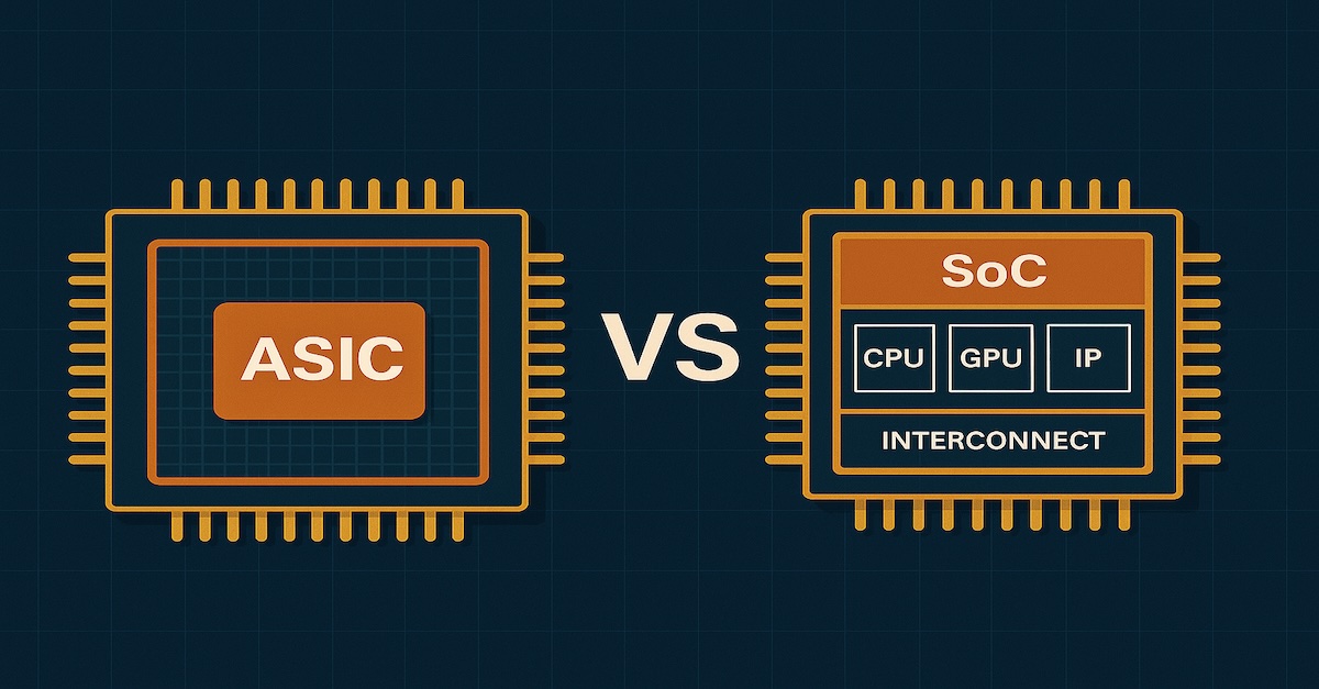
    What ASIC And SoC Actually Mean Today

    An ASIC was a fixed-function chip logic designed from scratch, optimized for area, power, and speed, and then locked down. It worked particularly well for high-volume products, where every bit of efficiency mattered.

    A System-On-A-Chip (SoC) integrates multiple functions, including CPU, memory controllers, accelerators, and I/Os, using pre-verified IP blocks. It reduced design time but gave up some control.

    The question is no longer “Is it an ASIC or SoC?” It is:

    • How much of it is reused?
    • How configurable is it?
    • How much control do you have?
    • Can team handle the integration and bring it up to speed?

    That line is now blurred. Most ASICs use third-party IPs. Some System-On-A-Chip (SoC) devices are heavily customized for specific applications. And hybrids, such as semi-custom SoCs and chiplet-based designs, mix both worlds.


    Design Tradeoffs: Cost, Time, And Risk

    The core difference between ASIC and SoC design is not technical. It is about tradeoffs. Engineering teams rarely get unlimited time, budget, or people. Every decision shifts pressure to another part of the process, resulting in more integration, extended verification, higher costs, or added schedule risk.

    ASICs and SoCs have different profiles in terms of cost structure, development time, silicon risk, and maintainability. These factors are not always apparent at the outset, especially when decision-makers prioritize performance or BOM reduction.

    The table below outlines the practical differences most teams encounter:

    FactorASIC DesignSoC Design
    Development Cost (NRE)High — Full RTL, physical design, verificationModerate — Uses licensed IPs and reference subsystems
    Licensing CostLow — Mostly in-house logicHigh — Paid IP cores (CPU, GPU, I/O, etc.)
    Time to MarketLong — Custom design and verification cycleShorter — Integration-focused, often platform-based
    Performance TuningHigh — Full control over timing and layoutLimited — IP black-box behavior restricts optimization
    Verification LoadFocused — Single-purpose, scoped verificationHeavy — Complex IP interactions and corner cases
    Risk of Re-spinHigh — Full custom logic, harder to catch bugsMedium — IP is usually well-tested but integration is risky
    Volume SuitabilityHigh — Payback improves with high unitsGood — Better for mid-volume or evolving product lines
    Design ReuseLow — Hard to adapt without major reworkHigh — Easier to reuse across multiple designs
    Team Skill RequirementAdvanced — Needs strong physical + logic teamMixed — Strong integration and system-level thinking
    Tooling/EDA DependencyHeavy — Full flow needed (RTL to GDSII)Shared — Platform vendors often provide part of toolchain

    Many teams attempt to strike a balance between the two, utilizing ASIC methodology for the core logic and incorporating SoC-style IP blocks around it. The key is not just choosing a design model but also knowing what your team can realistically deliver, verify, and provide production support for. Cost, time, and risk are always connected, improving one usually stresses the others.


    Post-Moore Constraints Are Changing The Game

    Shrinking nodes no longer guarantee better power, area, or speed. At 5nm and below, power density, interconnect delay, and thermal issues dominate. Routing is more challenging, and physical limits, such as variation and IR drop, can hinder performance gains.

    For ASICs, even finely tuned blocks now face yield and manufacturability challenges. Full-custom is harder to justify unless volumes are high. Teams increasingly rely on hardened IPs and foundry-guided flows to stay within constraints.

    SoCs handle this better through the reuse of mature IP blocks, stable interconnects, and known thermal profiles, thereby reducing risk. However, flexibility is limited. You cannot continually optimize data paths or packaging to fit specific system needs.

    In the post-Moore era, design is now more about managing limits than pushing specs. What matters is not what performs best in theory but what yields, scales, and ships reliably.


    Choose What You Can Sustain, Not Just What You Can Build

    The ASIC vs SoC decision is less about architecture and more about lifecycle cost, verification effort, and team maturity. If your design requires tight control over timing, power, or area and you have the resources to manage full RTL ownership, physical implementation, and signoff, ASIC can make sense.

    But every decision is expensive to change. One late bug or corner-case miss can delay the tape out or force a re-spin.

    SoCs reduce that risk by leveraging proven IP and platform integration. You trade off flexibility for predictability. But even that path demands strong system validation skills, especially when IP vendors vary in quality, methodology, and update cadence.

    The fundamental constraint is not what you can design, but rather what you can verify, debug, yield, and support under actual time and budget pressure. In a post-Moore landscape defined by complexity, cost, and uncertainty, sustainable execution beats architectural ambition. Choose accordingly.


  • The Semiconductor Value Of More-Than-Moore

    Photo by Dan Cristian Pădureț on Unsplash


    The semiconductor industry is all about value creation for the business dependent on it. This value is primarily due to Moore’s first law-driven semiconductor product that brought several generations of computing solutions. And, to ensure the value creation process continues forever, More-Than-Moore solutions are now needed.

    The need to bring More-Than-Moore is not due to Moore’s first law not applying to the semiconductor industry. More so, it is still a few decades before the semiconductor industry will run out of ways to pack more transistors while also shrinking the area.

    The fundamental reason to adopt More-Than-Moore solutions is Moore’s second law or Rock’s law, as it is known widely. According to it, the complexity and cost of a new generation of die solutions are doubling every few years and thus leading to a point whereby the ability to pack more transistors will not lead to any favorable cost benefits. The main reason is the capital-intensive semiconductor design, research, and manufacturing processes.

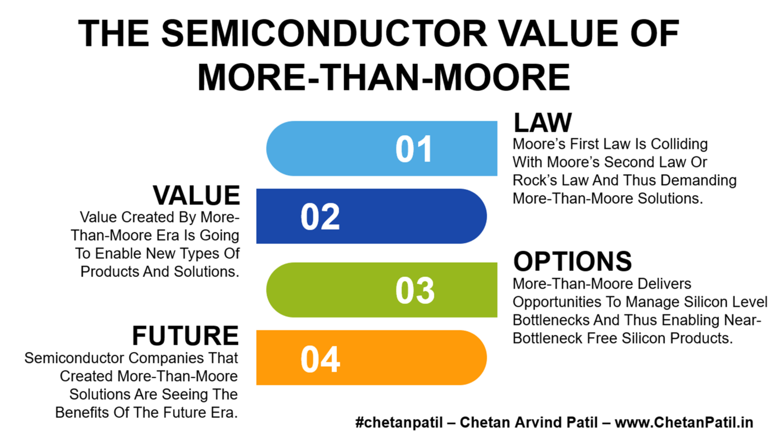
    Law: Moore’s First Law Is Colliding With Moore’s Second Law Or Rock’s Law And Thus Demanding More-Than-Moore Solutions.

    Value: Value Created By More-Than-Moore Era Is Going To Enable New Types Of Products And Solutions.

    The best way to overcome the scenario of Moore’s first law colliding with Moore’s second law or Rock’s law is to bring semiconductor solutions that speed up the growth of More-Than-Moore. It will enable a new generation of silicon products and balances the feature and costs of highly complex semiconductor products, mainly XPUs.

    Overall, the value created by the More-Than-Moore solutions is toward solving the exact problem the semiconductor design and manufacturing industry will face (or already has) in the future. More-Than-Moore provides design-level optimization and can also reduce the cost of manufacturing by leveraging the mix of older and newer technologies.


    Picture By Chetan Arvind Patil

    Today, complex silicon architectures are following the traditional die-level integration and hitting the feature walls, thus demanding new solutions. Something, More-Than-Moore can provide.

    Solutions like chiplets, disaggregated design, and heterogenous packaging are a few More-Than-Moore solutions. These solutions, for now, are costly. However, as the rate of adoption and deployment increases, the cost will slowly go down and eventually will drive new types of silicon solutions that are always bottleneck-free.

    Options: More-Than-Moore Delivers Opportunities To Manage Silicon Level Bottlenecks And Thus Enabling Near-Bottleneck Free Silicon Products.

    Future: Semiconductor Companies That Created More-Than-Moore Solutions Are Seeing The Benefits Of The Future Era.

    Out of all, a critical value created by the More-Than-Moore solutions is: providing options for the computing industry. Chiplets and heterogenous integration have already enabled this path. To further drive futuristic products, the semiconductor industry will have to focus on solutions that can provide customers with better options by embracing the More-Than-Moore-enabled era.

    Semiconductor companies that are working on complex silicon architecture have realized the value the More-Than-Moore era will bring. It is the primary reason such companies are investing in solutions that will become de-facto in the future. The companies that have not started working on such a solution should review the potential the More-Than-Moore era can provide by reshaping the computing world.