Category: OPINION

  • The Ever Changing Semiconductor Computing

    The Ever Changing Semiconductor Computing

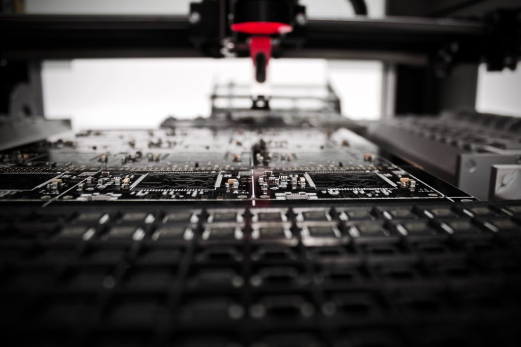
    Photo by Jeremy Bezanger on Unsplash


    THE FEATURES DRIVING SEMICONDUCTOR COMPUTING

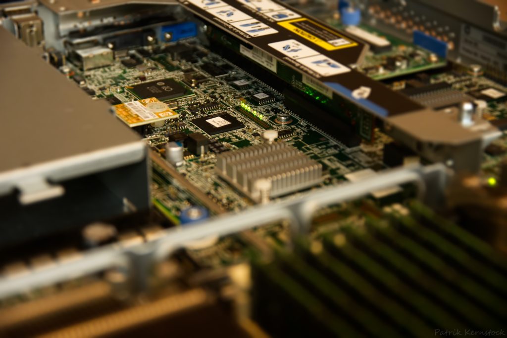
    The computing world is heavily reliant on semiconductor products. To implement target features, it is important to look into the low-level hardware characteristics. These characteristics over the years have become key driving factors and are not defining how future semiconductor-powered computing will be.

    The features that drive semiconductor computing are well known. These are a perfect combination of technical and business aspects. The business aspect focuses on increasing the margin apart from acquiring new markets and customers. The technical features set the foundation of how the computing system will work.

    The technical and business feature list is endless, but below few points define how key features drive the semiconductor-powered computing world.

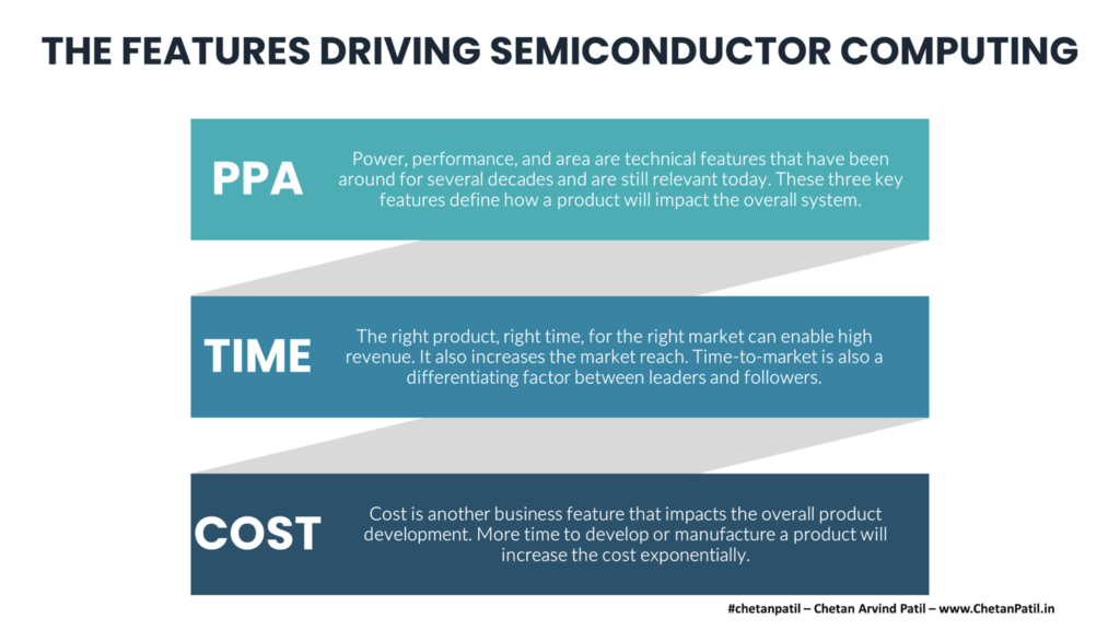
    PPA: Power, performance, and area are technical features that have been around for several decades and are still relevant today. These three key features define how a product will impact the overall system. As semiconductor technology has progressed, these three features have too. In the end, it all boils down to the different combinations of these three factors, which are required to power any given semiconductor computing system.

    Time: Time is a business feature, and it tracks the time required to bring the product into the market. The right product, right time, for the right market can enable high revenue. It also increases the market reach. In a highly competitive world like the semiconductor industry, the time has been a differentiating factor between leaders and followers.

    Cost: Cost is another business feature that impacts the overall product development. More time to develop or manufacture a product will increase the cost exponentially. New semiconductor technologies like FETs, Packaging, and Testing also have increased the cost of product development.

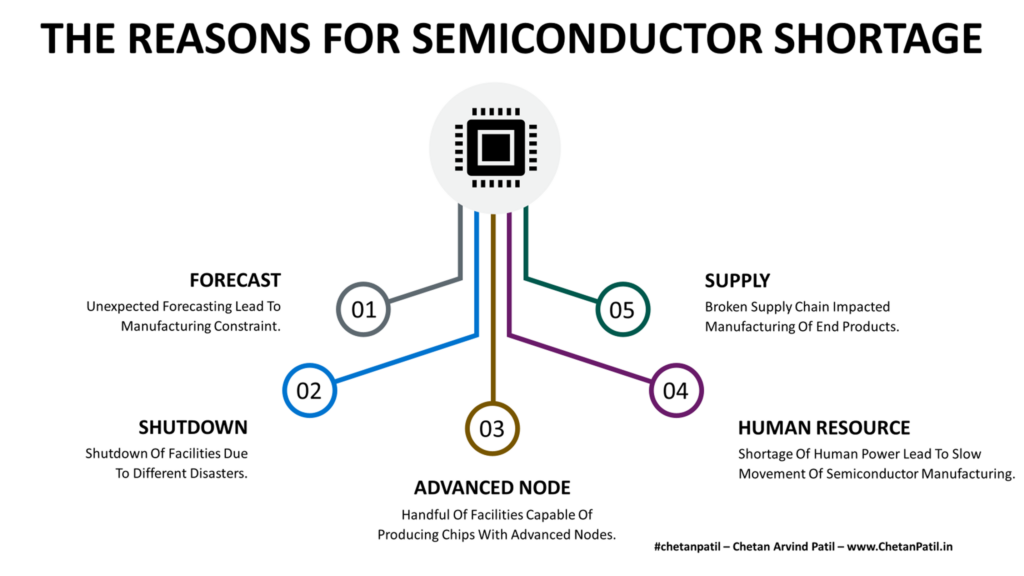
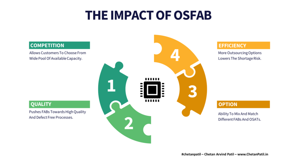
    Two critical changes have occurred in approximately the last two years: First is the increasing complexity of the semiconductor products that power the computing world (XPUs etc.). Second is the resources required to bring the complex features into the market. 

    The complexity comes as part of providing modern features. The resources aspect (non-human) is something that has an impact on semiconductor computing. The reason is the CapEx-driven facilities and continuous investment required to drive next-gen semiconductor computing.


    Picture By Chetan Arvind Patil

    Picture By Chetan Arvind Patil

    THE NEXT-GEN SEMICONDUCTOR COMPUTING FEATURES

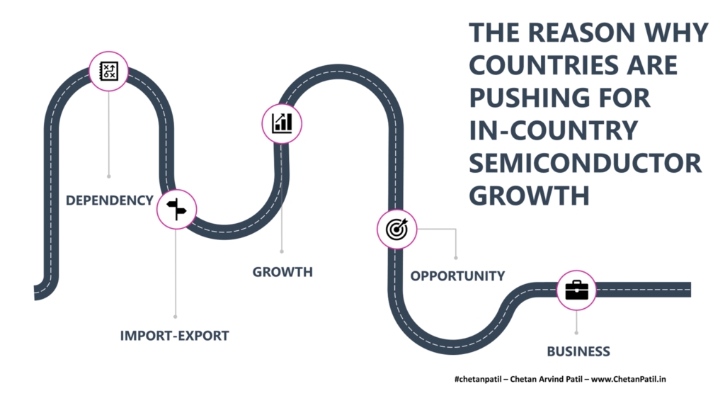
    The world of computing is advancing. The need to provide modern semiconductor-powered systems is never going to end. To meet customer (and market) demand, the semiconductor industry has to keep inventing next-gen features.

    The semiconductor industry has already been inventing new technologies for decades and thus pushing the computing industry forward. These features have followed Moore’s law, and several got launched due to the market demand.

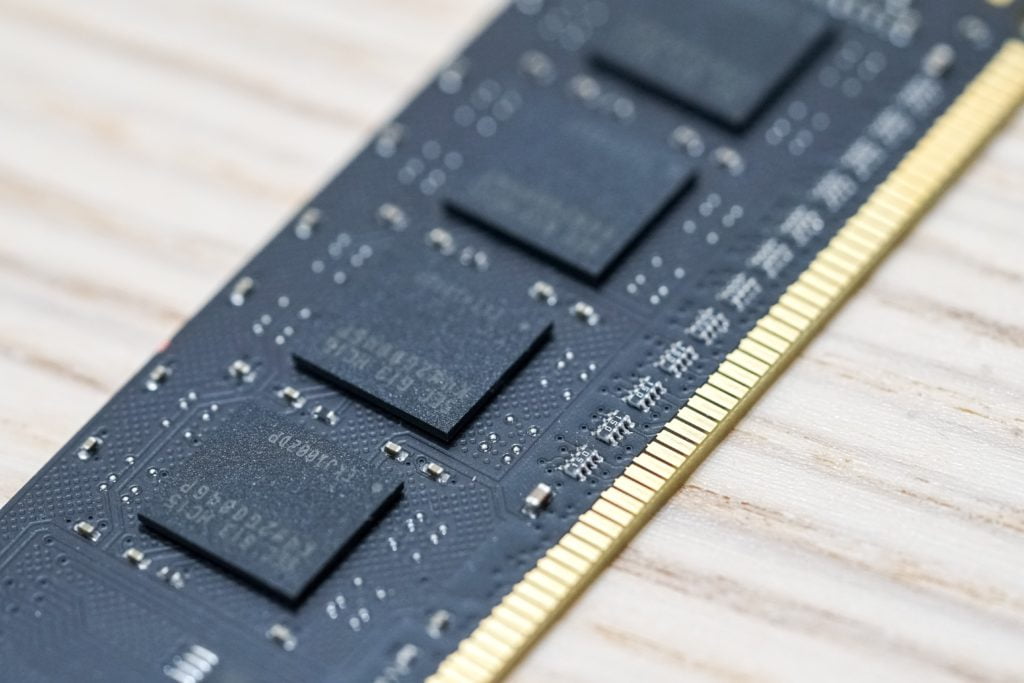
    FET: FETs are the building blocks of any silicon chip. Several transformational changes have occurred around FETs. However, the angstrom era demands a new wave of FETs that can drive the critical components (XPUs and other similar chips) towards power and performance needs that can drive next-gen semiconductor needs. These can be from better operating to area requirements.

    Package: Like FETs, package technology has to evolve. While several advanced packaging solutions already exist, there are still new features required to manage the complexity of the new generation of design methodologies like chiplets brings-in. On top of all this, package technology also has to be cost-effective, otherwise, the cost of manufacturing will keep rising.

    Adaptive: Workloads are getting complex year-on-year. Constant architecture processing these new workloads often ends up with bottlenecks. Design and manufacturing approaches for chips targeted for the computing industry needs to be more adaptive. Neural Processing Units (NPUs) provide a way forward, but still, a lot of work is required to make it mass-market friendly.

    The computing world is going through drastic changes. Customers want a balance of power and performance to drive savings without impacting features. Balancing these two features is not an easy task. That is why next-gen features like FETs, package technologies, and adaptive will play a key role in shaping up the semiconductor-powered computing industry for the decades to come.

    Apart from features, drastic changes in design and manufacturing methodologies are also two key pieces that will drive next-gen semiconductor computing features. All this will heavily rely on how the existing and emerging semiconductor companies bring in the new solutions.


  • The Semiconductor Manufacturing Cluster

    The Semiconductor Manufacturing Cluster

    Photo by Louis Reed on Unsplash


    THE REASONS TO DEVELOP SEMICONDUCTOR MANUFACTURING CLUSTER

    Developing a dedicated semiconductor manufacturing infrastructure from scratch is a billion-dollar risk and the cost of doing so is also increasing year on year. As the semiconductor industry marches towards a new era of capacity creation, it is important to invest in strategies that can enable a high return on investment.

    Today, the majority of the big semiconductor manufacturing companies are looking for new regions to create their next-gen semiconductor device fabrication, assembly, and testing infrastructure. The cost of making the wrong choice for such a large investment is very high.

    The time, and effort required to build semiconductor manufacturing infrastructure are pushing companies, and also governments, towards utilizing (or creating) regions that already have a semiconductor history. This is one of the major reasons why companies like TSMC, Intel, and Samsung are focusing on regions that already have a large presence of semiconductor companies (end-to-end), as it allows them to make the most of the existing ecosystem and thus drives their new facilities towards breakeven.

    Semiconductor Manufacturing Cluster: A dedicated region or area, where within proximity different semiconductor companies have facilities to provide semiconductor device fabrication, assembly, testing, and distribution services. This area may and may not house a different number of semiconductor design companies.

    When multiple semiconductor manufacturing companies are located in the same region, then a semiconductor manufacturing cluster is formed. A semiconductor manufacturing cluster provides several benefits. These benefits are more geared towards semiconductor companies but in the end also benefit the city or the region where these clusters are located.

    Collaboration: A region with multiple semiconductor manufacturing (and design) companies enables collaboration that can drive the development of next-gen solutions and thus benefits the semiconductor industry at large.

    Optimization: Semiconductor manufacturing cluster will allows the development of several business resources that can aid companies. This can range from raw materials to near-by equipment provider to several other support systems that semiconductor manufacturing companies often need.

    Research And Development: The proximity of advanced semiconductor manufacturing facilities allows companies to develop research and development infrastructure. This is often in collaboration with the government and universities. Doing so speeds up development of new devices that can provide much better efficiency and thus pushes the development of new semiconductor-driven products.

    Ecosystem: Worldwide, there are different semiconductor manufacturing clusters. Some are in Taiwan, some in China, and many in the USA. All these regions have transformed themselves into powerhouses and are now an ecosystem for emerging semiconductor manufacturing facilities.

    Talent: In the end, human resources are vital for any industry. The same applies to the semiconductor manufacturing facilities wherein different skills are required to drive the development of semiconductor products. Semiconductor manufacturing cluster creates an infrastructure that attracts talents from all over the world.

    Semiconductor manufacturing clusters are not built overnight. It takes years of effort from both the government and private players. In many cases, a single entity starts from scratch and there on goes on attracting future companies. There on, over an extended period creates the semiconductor manufacturing cluster on its own. Also, having a university with a very high research and development focus is also an important factor in driving cluster-based semiconductor manufacturing regions.

    Worldwide, as governments attract new investments towards semiconductor manufacturing, it is worth planning by focusing on strategies that can eventually turn the regions into a semiconductor manufacturing cluster.


    Picture By Chetan Arvind Patil

    Picture By Chetan Arvind Patil

    THE STEPS TO BUILDING SEMICONDUCTOR MANUFACTURING CLUSTER

    Developing a dedicated semiconductor manufacturing cluster is not an easy task. It takes years of planning, investment, collaboration, failure, and risk to create one. This is the primary reason as to why there are only a handful of countries that have semiconductor manufacturing clusters.

    Semiconductor clusters can be classified into two types:

    Multiple Companies Multiple Facilities (MCMF): A specific region where multiple semiconductor manufacturing companies come together to create their own separate semiconductor manufacturing infrastructure to drive device fabrication, assembly, and testing.

    Multiple Companies Single Facility (MCSF): A specific area or a region where multiple semiconductor manufacturing companies invest to create a single large facility to provide fabrication, assembly, and testing services for different semiconductor companies.

    MCMF is very common and countries like Taiwan, Japan, South Korea, China, and the USA already have several such regions which cater to different needs of semiconductor manufacturing.

    On another hand, MCSF is very rare and the major reason is the effort required to bring different stakeholders to invest in a single facility that can cater to the manufacturing requirements of different semiconductor players. Today, planning for MCSF might be more favorable due to the cost and time, but there have been several examples where such collaborative strategies have failed.

    Countries looking to develop a region that purely focuses on semiconductor manufacturing need to plan for the next century and not a decade, and the following steps can provide a roadmap of achieving the goal of developing a semiconductor manufacturing cluster, which is what countries without semiconductor manufacturing history need today.

    Government Support: Government support is crucial in driving the development of policies, incentives, and facilities that can cater to the semiconductor manufacturing cluster. This is why countries looking to attract new semiconductor manufacturing investment should develop strategies to make an investment from private players a long-term collaboration.

    Private Partnerships: Semiconductor manufacturing clusters today will require move JV between different semiconductor companies. While single entities can themselves invest in new FABs and OSATs, but in the long run, the region needs to develop by continuously attracting new investment. This is possible if in the initial phases more JVs are formed to drive the development of the semiconductor manufacturing cluster that future private players can take advantage of.

    Aligned Goals: Both government and private players need to be on the same page so that the region chosen as a dedicated place to develop the next-gen cluster thrives for several decades. This requires not only planning for the semiconductor industry but also building regional facilities like logistics to universities and several other plans to drive day-to-day facilities. 

    Future Roadmap: In the end, dedicated clusters are divided into sub-regions that are owned and operated by different entities. However, if there is no future roadmap as to why several companies are bringing new investment (mainly if the cluster type is MCSF) then the future roadmap may not be beneficial. Hence, companies need to collaborate more to drive new manufacturing methodologies.

    Continuous Investment: Semiconductor manufacturing clusters are difficult to build and to make the most of it, continuous investment is required. This can be in the form of new investment policies from governments to attract new semiconductor companies to build new facilities (example: TSMC in Arizona) that can take the region towards a new era.

    There are multiple ways of attracting new investment into new regions/countries. Semiconductor manufacturing cluster vision and planning is one of doing so. This way, semiconductor companies (focused on manufacturing) can be confident in the future of the location they are investing in.

    Whether, the semiconductor manufacturing cluster is MCMF or MCSF, the benefits of regions with multiple semiconductor companies are profound, and governments all over the world should focus on developing semiconductor manufacturing clusters to facilitate in-country requirements of future semiconductor products.


  • The Reasons And Mitigation Plan For Semiconductor Shortage

    The Reasons And Mitigation Plan For Semiconductor Shortage

    Photo by Marc PEZIN on Unsplash


    THE REASONS FOR SEMICONDUCTOR SHORTAGE

    In today’s market, the majority of the consumer and enterprise products are heavily equipped with semiconductor products (silicon chips). Over the last few years, the share of semiconductors in modern products has increased steadily. From automotive to smartphone to smart devices to aerospace, everywhere semiconductors are present. This has made semiconductors the building blocks of modern infrastructure.

    These semiconductor products (silicon chips) require a lot of precision and time to manufacture. Any gaps in the manufacturing flow can eventually have negative consequences, which not only has an impact on the semiconductor manufacturers but also on the end products that are using these tiny silicon’s, and this is exactly what is happening since 2020.

    Semiconductor Shortage Is A Combination Of Both The Design And The Manufacturing.

    Shortage in the semiconductor industry not only impacts the semiconductor industry itself, but it ends up costing a lot to all the companies that are heavily reliant on these products. This is why automotive production has been halted, consumer electronics are not available easily in the market, and many other several consequences.

    So, what is the reason for the semiconductor shortage?

    Shortage in the semiconductor products is not because of one specific reason. To stop an industry like semiconductor from manufacturing, several negative factors have to come together. Unfortunately, this is what has lead to the shortage of semiconductors as the factors affecting it have introduced gaps in the manufacturing flow.

    Below are the major contributing factors for the semiconductor shortage:

    Forecast: Forecasting is an important part of ensuring that there is no wastage and all the customer demands are met in time. This eventually leads to efficient supply chain management. However, the forecast is not always accurate. It relies on many factors. This can range from market demand, a customer moving to a new solution, better cost alternative, and many more. For the semiconductor shortage that started in 2020, the reasons are majorly due to the market demand. Due to COVID-19, several facilities have to be closed down and this forced consumers and businesses to work remotely. This leads to the sudden surge in demand for smart solutions (one of the several such surges) and eventually increased the semiconductor demand (breaking the forecast). This prompted the companies to play safe by stocking (manufacturing) more devices than planned, which eventually put pressured on the semiconductor manufacturing capacity which lead to slow movement of silicon development, eventually putting them through the tough time of managing never seen before capacity management.

    Shutdown: Semiconductor FABs are designed to run 24×7. The facilities are so complicated that any kind of shutdown can take weeks to recover, and will eventually lead to a shortage in silicon chip delivery which in turn halts the product of several other dependent industries (automotive for example). This exactly is what has happened in the last few months. Some FAB has to be shut down due to COVID-19, some due to extreme weather climate, and few due to fire hazards. All the FABs that were impacted were large facilities catering to the core products/solutions. Once a shutdown happens it becomes difficult to re-run the FAB quickly without proper checks to ensure there are no blocking points during the manufacturing flow.

    Advanced Node: A smart product is made of different electronic chips. Each of these chips is using a different technology-node. However, the smartest and the most critical pieces in these devices are using the most sophisticated technology-node out in the market. Unfortunately, there are not many semiconductor FABs that are making advanced nodes. This puts a lot of dependency on these FABs and any shortfall in the production is eventually going to have an impact on the end product. The surge in demand in one segment (relying on the advanced node) has lead to a shortage of silicon products (using advanced node) in the other market segment. There is no time to expand the facility and this has eventually lead to the shortage of advanced node silicon.

    Human Resource: Semiconductor FAB is highly automated but eventually does require human intervention. There are several tasks that have to be carried out manually and all these tasks are part of building the production wafers. COVID-19 lead to the curtailing (for their own safety) of people inside the FAB and this slowed down the production movement. The slowing of FABs is not good for the industry relying on semiconductor products. This eventually leads to slow production and contributed to the shortage.

    Supply: Supply is not only about shipping the semiconductor product out of the FAB. It is also about ensuring the wafers and assembled part keep moving ahead till the end product has been assembled. Unless and until all the silicon chips are available, the end product (television for example) cannot be assembled. The semiconductor shortage is not about all the silicon products that go insider a device (for example smart camera), it is more about several other components that come from different FABs and facilities. Any supply constrains any of one the supply points can introduce shortage.

    The above points are a handful amount of reasons. In reality, there can be more valid reasons for the shortage. In the long run, the semiconductor industry will overcome all the shortages and will also learn from them.


    Picture By Chetan Arvind Patil

    Picture By Chetan Arvind Patil

    THE MITIGATION PLAN FOR SEMICONDUCTOR SHORTAGE

    Shortage of any product (groceries to cars to semiconductor) eventually does get over. It indeed takes time and also leaves behind learnings that should be leveraged to overcome any such scenario in the near term.

    When it comes to a high-tech industry like semiconductors, there is no single answer to semiconductor shortage avoidance. The shortage in the first place was contributed due to many factors. Based on the market situation below are the few points that can help mitigate the shortage in the future:

    Older Node: Moving all the critical semiconductor solutions to the advanced node without building capacity is not the way forward. The FAB-LESS/IDM semiconductor design houses have to go back to the drawing board and understand how to diversify the technology-node usage based on the available capacity. Of course, the technology combination should eventually meet the specification, but the end goal should be to also consider how the market capacity (reality) is and will there be any capacity constraint if different shortage reasons come together again in the near future.

    Internal Capacity: While IDMs already have the internal capacity that they can leverage to capture sudden increase in semiconductor demand. However, there needs to be a thorough review of what type (solutions) of capacity is in-house and how to balance the capacity against the external one. This can allow any of the external capacity shortages to be absorbed internally and thus helps in mitigating any pitfall.

    Backup: Semiconductor products eventually get tied to a specific manufacturing flow that includes FABs and OSATs. It takes years to move these products to newer facilities. This is why semiconductor companies should start qualifying their products for multiple facilities to ensure any gaps/shortage at one location is fulfilled by the backup option.

    External Capacity: Pure-Play foundries are very crucial to the semiconductor industry. They play an important part in ensuring that the product meets the end customers’ demand. However, in the last couple of decades, there has been growing reliance on external capacity. There is nothing wrong with it and not all semiconductor companies can put so much money in the semiconductor FAB. Still, the problem arises when there is a constraint in the external capacity as external can be pre-booked or pre-occupied by any entity in the world. This puts pressure on other semiconductor design houses that rely on external capacity but do not have enough capacity pre-booked. This has promoted an important discussion to build more external capacity that caters to not only today’s demand but to the demand of the next few decades.

    Modularity: Both the design houses and the manufacturing facilities will have to quickly adapt to the modular approach. This modular approach can be about using any technology-node possible and also using any semiconductor manufacturing facility that is available. This will be a daunting task but should be doable.

    Semiconductor design and manufacturing both play a crucial role in product development. Shortage in the semiconductor product is not only about the manufacturing but also about the design constraint that hinders flexibility in the manufacturing flow.

    This is why the semiconductor shortage in 2020/2021 should not only be seen from the manufacturing aspect but also from the design point of view too.


  • The Semiconductor OSFAB

    The Semiconductor OSFAB

    Photo by Patrik Kernstock on Unsplash


    THE ROLE OF OSFAB

    In the majority of the industry, outsourcing enables a way to operate efficiently. The efficiency is achieved both from a technical and business point of view.

    In the software industry, outsourcing is primarily focused on providing the right tools and services required to drive internal day-to-day operational activities efficiently. This allows the customer (companies) to instead focus on their core business. The same outsourcing strategies are applicable in the hardware industry, in some cases more than it is in the software industry.

    The core business of the semiconductor chip design companies is to come up with designs that allow them to create products for their niche market. In many cases, semiconductor companies often have to compete with others to win the business. To drive winning strategies, no matter what, the semiconductor companies have to focus on the manufacturing process. Without manufacturing and delivering samples on time, there is no way to win the market. This is why companies without in-house semiconductor fabrication facilities (FAB-LESS) have to heavily rely on OSFAB.

    Outsourced Semiconductor Fabrication (OSFAB) is not new to the semiconductor industry. Companies like TSMC, Samsung, and alike have been providing OSFAB services to the semiconductor industry for a long time. In doing so, these companies have created a niche market for themselves. And, over the years as the OSFAB business has grown, they have also added the required capacity. Another advantage OSFAB provides to FAB-LESS companies is the option to choose from a large pool of technology-node and industrial flow options. This allows FAB-LESS (and in some cases also to IDMs) a way to optimize and allocate products to different OSFAB.

    Even though OSFAB has been critical to the semiconductor industry, there seems to have a growing reliance on specific OSFAB companies. If the trend continues, then there will not only be a shortage of OSFAB (due to growing semiconductors in different products) but the dependency might harm the semiconductor companies without any internal FAB capacity.

    Recently, Intel announced IFS (Intel Foundry Services), which will open up Intel’s FAB capacity to the outside world. This is a welcome change in many aspects. Foremost, it will put pressure on companies that have dominated the OSFAB arena. It will also drive new manufacturing solutions (devices, FETs, AI-driven automated processes, etc.) that will eventually help the semiconductor industry.

    Intel’s years of design and manufacturing experience will also have an impact on the cost and capacity strategies that many of the FAB-LESS often have to focus on.

    Cost: The top FAB-LESS companies are well capable of spending and building internal FAB capacity. However, they do not do so due to the added CapEx and operating cost. With Intel joining the OSFAB business along with TSMC, Samsung, and others, the ability to optimize cost will only increase. This cost can be from taking advantage of Intel’s process node that is different (and maybe in some cases better) than its rivals but is low on cost. FAB-LESS companies can also deploy strategies to prioritize products based on the time-to-market and thus evaluating non-critical products at the new OSFAB to capture how much cost optimization can be achieved.

    Capacity: The worldwide OSFAB capacity increase due to Intel Foundry Services will provide FAB-LESS with options to choose from and thus will allow them to allocate products to different OSFABs. This will take away the pressure of planning years in advance and also ensuring that there is no dependency on specific OSFAB. On top of all this, newly added capacity also provides companies with an option to choose the OSFAB that is more supply chain friendly.

    OSFAB business is going to heat up more in the coming years. In the next couple of years, TSMC, Samsung, Intel, and others will be competing against each other and this will only allow FAB-LESS companies to leverage the best semiconductor manufacturing solution in the market.


    Picture By Chetan Arvind Patil

    Picture By Chetan Arvind Patil

    THE IMPACT OF OSFAB

    Irrespective of how Intel’s new Foundry Services shapes up the semiconductor industry, there is certainly a positive impact of OSFAB. Since the OSFAB business is primarily focused on providing cutting-edge solutions to the semiconductor design houses, the internal research and development activities end up providing nice solutions to the market.

    OSFAB without having to focus on the design aspect of any product they manufacture, end up spending a lot of time and money in perfecting the manufacturing process. This eventually pushes the industry towards next-gen products that are more efficient and at the same time powerful enough to meet the target application needs.

    To summarize, there are four major aspects (mix of technical and business) that OSFAB drive:

    Competition: The more OSFAB options are there in the market the better it is more the end-customer i.e. FAB-LESS. FAB-LESS companies get an edge to choose from different capacity that is available in the market. From the OSFAB point of view, it is a good scenario too as it pushes competition and it ends up driving new products (FETs/devices) that can be vital in attracting a new customer base. If there is no competition and the only couple of big players have all the OSFAB capacity, then the pace of innovation will slow down. This is why Intel’s decision to open up its FAB is going to not only add pressure on the OSFAB business but will also push OSFAB towards newer FET devices.

    Quality: OSFAB focuses primarily on the manufacturing aspect of the semiconductor. Doing so allows them to deploy strategies and solutions that ensure defect-free products. In a semiconductor, where the room for error is next to none, maintain high quality is the topmost criteria. The quality control can come from an error-free fabrication pipeline or by deploying equipment/tools that capture defects early in the fabrication line. OSFAB has played a critical role in enabling such a solution.

    Option: Having OSFAB also provides options to FAB-LESS companies to mix and match the FAB with different OSAT. This allows them to diversify key products from a supply chain point of view. Depending on specific FAB/OSAT can have a negative impact. With growing OSFAB capacity, it is becoming a more business-friendly option for FAB-LESS companies, as it will allow them to plan products and in many cases execute them in parallel instead of waiting for capacity to open up.

    Efficiency: Having more OSFAB options (along with new capacity added by TSMC, Intel, and even Bosch in automotive) ensures there is never a shortage of FAB to choose from. If OSFAB X is fully occupied then the FAB-LESS can certainly take advantage of OSFAB Y. In many cases, going for newer OSFAB can bring better (and future capacity) options. This frees FAB-LESS companies from planning and securing capacity and instead puts energy on how to execute products for the market.

    Both OSFAB and OSAT play a crucial role in bringing design to life. Eventually, adding more capacity is only going to drive the competition and also provide FAB-LESS with more options. It is also a vital time for countries without OSFAB to start building one today (at least for internal consumption).

    Hopefully, Intel’s new announcement is only going to have a positive impact and will push the semiconductor industry towards newer semiconductor manufacturing solutions.


  • The Roadmap For In-Country End-To-End Semiconductor Industry Growth

    The Roadmap For In-Country End-To-End Semiconductor Industry Growth

    Photo by Laura Ockel on Unsplash


    THE REASON WHY COUNTRIES ARE PUSHING IN-COUNTRY SEMICONDUCTOR GROWTH

    The basic and the applied science form the base for any technological advancement. Countries globally have always focused on the importance of these two aspects of science. That is why countries race against each other and invest a lot of time and money to lead science that enables technology.

    In the 21st century, the focus on applied science (basic science is not behind, maybe ahead in several aspects) skyrocketed due to the proliferation of digital devices and wireless connectivity. Only a handful of countries quickly realized the importance of leading in a technological solutions that forms that base of a modern digital solution. Some focused heavily on the research and development (design) of novel technologies (WiFi to 5G to autonomous to robotics and beyond), while others emphasized the need to manufacture these for the end customers.

    Semiconductors Are Everywhere

    The semiconductor industry also can be seen by separating out into design and manufacturing. Countries like the USA focused more on the design aspect of the semiconductor, while Taiwan and China ramped up manufacturing efforts. This worked well until the 5G and COVID raised concerns over the growing inter-dependency, and then started the saga of how leadership in the semiconductor design and manufacturing affects day-to-day technological (from satellites to cars) solutions. This in turn started pushing several other countries (India to Australia and beyond) to focus on the need to design and manufacture semiconductors in-country.

    There are several reasons as to why countries (which are behind) should focus on end-to-end in-country semiconductor industry (or at least have enough infrastructure to cater to in-country demand):

    Dependency: Relying on other regions for manufacturing or designing semiconductor products is one reason that is pushing countries to focus on the in-country end-to-end semiconductor solutions. This also includes materials to equipment. It is difficult to make everything in-house, hence good enough infrastructure to cater to the local consumer demand and critical national infrastructure of the county is a good way to start.

    Import-Export: From smartphones to cars, all are heavily powered by semiconductor solutions. In trade, it is good to keep imports and exports in balance. Countries without vital semiconductor (manufacturing) infrastructure will always end up importing more than exporting. This will put pressure on their forex reserves and will make them fully dependent.

    Growth: The semiconductor market is growing due to the growth of semiconductor usage in the modern infrastructure/technology. Automotive is one example, apart from the consumer market, and many other industries where semiconductor solutions are used by default. Countries should capture a portion of the market which will eventually generate employment and business growth. This is critical for long-term financial stability too.

    Business: Establishing a high-tech industry like semiconductors (mainly manufacturing, as many countries do have design houses) will not only lead to market growth and employment but will also support other businesses that eventually are the pillars for the semiconductor industry. It can be from equipment manufacturing to raw materials to turn-key (and ever-expanding) civil engineering work to build FABs/OSATs.

    Above points fueled with the growing use of semiconductor in all the major infrastructures and technological solutions (that affects every aspect of day-to-day life) is more than enough reasons for countries with lacking semiconductor manufacturing infrastructure to start today for tomorrow’s need.


    Picture By Chetan Arvind Patil

    THE ROADMAP FOR IN-COUNTRY SEMICONDUCTOR INDUSTRY SUCCESS

    There are 195 countries and each one of these have their own strengths and weaknesses. It is difficult to create an end-to-end in-house solutions for the semiconductor industry. More so, when the goal is to drive in-country semiconductor growth to the next level.

    In reality, there are no roadmaps that countries can follow to gain momentum for an in-country semiconductor to make themselves self-reliant. On other hand, countries today also cannot overlook the importance of having as many points checked from the roadmap that can enable, if not end-to-end, some parts of the semiconductor supply chain. This will allow them to tap into the future market needs and ensure stability in semiconductor market.

    The roadmap to success in the semiconductor industry consists of many points and below are the few major ones:

    Talent: Nothing can be developed without having the right set of talent (human resources). Countries already have a framework to educate their population. However, the traditional education system is still focusing on core aspects that enable basic training. While there is no harm in doing so, it is about time that countries wanting to engage in in-country semiconductor growth (manufacturing and beyond), needs to start with training programs that focus more on core semiconductor on-field training programs apart from the fundamentals.

    Policy: Eventually, investment is a big part of semiconductor growth. While countries looking to steer ahead in the in-country semiconductor solutions have already started to come up with incentives and policies, the approach should be more holistic that focuses not only on the semiconductor growth but also on the regional infrastructure required for the semiconductors. This may be from ensuring airports to logistics to man-power availability, apart from ease of the land and housing facilities.

    Infrastructure: The semiconductor supply chain is heavily driven by the turn-key infrastructure. From FAB-LESS to FABs to OSATs, all require support infrastructure to ensure the products reach the market in time. This infrastructure varies from material handling to chemicals transportation to water availability to non-stop electricity. Building FAB/OSAT is one thing and running it non-stop is another. The better the support infrastructure for the semiconductor industry, the more likelihood of semiconductor giants willing to setup future-focused manufacturing setups.

    Public-Private: Government support plays a very key role in driving in-country semiconductor growth. This can be from investing in the required infrastructure to providing incentives that can ensure required investment is available to drive manufacturing facilities. A two-way shake hand between the private players and public bodies can drive the needed policies that are friendly to both the businesses and the consumers.

    Research: Research is key to long-term semiconductor growth. Countries focusing on the in-country semiconductor ecosystem should provide research funding (mainly countries with lack research funding support) to universities and colleges to focus on the next-gen semiconductor devices and manufacturing solutions. Universities and colleges themselves also can raise funding via industry collaboration with the semiconductor companies.

    Academia: Education is vital to every aspect of industrialization. The majority of the countries already have the infrastructure to educate the future workforce. However, the goal to make semiconductor in-country growth requires academic institutes to focus on semiconductor engineering courses apart from the traditional engineering domains.

    Cluster: FAB requires billions of dollars before it can run at full capacity and then it takes years to break even. Even then, due to changing technology-node and solutions around it, the process to upgrade FAB is a continuous one. Countries without a FAB wanting to attract/setup one, should focus more on the cluster approach. Cluster-based FAB can be a pooled investment for higher technology-node (older but relevant) that caters to different semiconductor FAB-LESS companies. Such kickstart can then lay the foundation of dedicated sub-10nm foundries.

    Outreach: Outreach is about reaching out to other countries and also attracting businesses to showcase what a specific country can offer. This way there is a dialog between the public and private players that can lead to many business opportunities in the semiconductor sector. Countries should do outreach by default, if the goal is to setup the semiconductor manufacturing (FABs to OSATs) in-country.

    Future-Tech: Countries that have semiconductor design houses but not manufacturing facilities should set the target on what the world will need in 2040 and not in 2030. This can range from chiplets manufacturing (semiconductor specific) to next-gen 6G wireless solutions to flexible electronics. Doing so will ensure that the companies and countries are creating infrastructure today for tomorrow’s demand. This can give an edge over countries with massive semiconductor manufacturing infrastructure and are not willing to invest further without closing/upgrading existing semiconductor infrastructure.

    The above roadmap points cover the majority of the aspect of ensuring in-country success in the semiconductor industry. There can be different points that also are vital for the semiconductor industry growth. In the end, it all boils down to what eventually works and what does not.


    Picture By Chetan Arvind Patil

    THE LONG TERM IMPACT OF IN-COUNTRY SEMICONDUCTOR INDUSTRY

    The last two years have shown the growing importance and emphasis on the need for in-country semiconductor industry growth. Countries are putting efforts to lead in every aspect of the semiconductor solutions, mainly in order to make themselves less reliant on other countries while also taking lead in the advanced modern technological solutions.

    The in-country semiconductor growth will have two major long term impact:

    Self-Reliance: Countries that can take the lead in the semiconductor industry growth will make themselves self-reliant in the long term. Which will prove vital in the long term due to the fact that the consumers solutions to national infrastructure is fully reliant on the semiconductor powered solutions.

    Leadership: There is no denying that every country is racing to claim leadership in every aspect of the modern world. Leadership in the semiconductor industry is certainly going to veto on who gets to call itself the superpower.

    It is good that the semiconductor industry is getting the focus, but countries will have to be diligent in understanding what works and what does not works as per the demand and supply requirements.

    In the end, investment to get semiconductor manufacturing up and running is huge. Any miss-step will put countries behind instead of going ahead. It also takes years of planning to create any kind of massive (and advanced) infrastructure.

    Hopefully, the global supply chain the semiconductor industry runs on, stays intact even with in-country semiconductor infrastructure race.


  • Indian Automotive Industry Can Drive Semiconductor Manufacturing In India

    Photo by Amin Khorsand on Unsplash

    India’s automotive industry is the world’s largest two-wheeler, three-wheeler, and tractor manufacturer. It is also the world’s second-largest bus manufacturer, third-largest heavy truck manufacturer, and fourth-largest car manufacturer.

    With the advancement in automotive solutions that will enable sensor-based safe assisted driving, the demand for smart Electronic Component Units (ECUs) will grow for every car, tractors, trucks, buses, and motorcycles that will come out of India’s production unit. Smart semiconductor products have started to change the automotive industry for good.

    Picture By Chetan Arvind Patil

    With the growing demand for automotive vehicles in India and the ability to export it in different regions, isn’t it time to ensure that the semiconductor products that are drivers of smart capabilities are also manufactured in India?

    The fairly old and well established automotive industry can surely enable semiconductor manufacturing growth given the increasing demand for smart solutions from infotainment to radar to collision avoidance.

    It is being anticipated that in 2030, 80% of the cars driving capability will be based on smart ECUs. Rest 20% will depend on the rules and regulation around level 5 is autonomy.


    AUTOMOTIVE INDUSTRY IN INDIA

    India has set an ambitious goal to move to alternate-fuels for automotive. First step is 100% electric cars only by 2030. This also means increased demand for semiconductor products that make up the smart ECUs to enable efficient driving.

    With each new car having more feature than the last one and all of these features relying on semiconductor solutions, raises the question of how automotive industry can drive semiconductor manufacturing in India.

    A very crucial and vital role will be played by the Original Equipment Manufacturers (OEMs). India is already home to all of the top automobile manufacturers that are evenly spread across different clusters and states.

    India Will Be The World’s Third-Largest Automobile Manufacturer With A Market Size of $300 Billion By 2026.

    Picture By Chetan Arvind Patil

    Designing of automotive ECUs is actively done in many of the R&D offices by the semiconductor companies in India. However, the majority of these smart solutions are manufactured overseas and then imported by automotive customers back in India.

    If all the activities from design to manufacturing of semiconductor products for the auto industry is done in house in India, then the benefits in terms of employment and business are huge.

    Any advanced car that is manufactured in 2020, has around 100 million lines of software code that has to meet automotive regulation. The established software industry in India can then provide over the top (OTT) solutions that will quadruple the amount of safety features on top of the smart mobility solution provided by the semiconductor solutions.


    LEADERS IN SEMICONDUCTOR AUTOMOTIVE SOLUTIONS

    Currently, the leaders in semiconductor manufacturing for the auto industry are all based in the Americas, EU, or East Asia. India certainly is home to all these semiconductor giants but only from designing and R&D point of view, which in itself is a great advantage.

    The automobile industry’s growing demand for smart semiconductor solutions in India should be an attractive opportunity. Establishing semiconductor manufacturing units in India not only allows semiconductor design companies to have access to the automobile industry but can also enable the growth of other sectors that they are catering to apart from the auto industry in India.

    Having an end-to-end design to manufacturing solutions in India will also help companies innovate faster and enable cost savings without compromising on security and quality.

    Another important factor is India’s open market that already has a talent pool to drive innovation. Many companies already heavily invested in R&D activities that can then quickly be tested using the automotive infrastructure.


    SEMICONDUCTOR AUTOMOTIVE OPPORTUNITIES

    As per Deloitte, the cost contribution of automotive electronics in 2007 was 20% and in 2017 it increases to 40%, and by 2030 it is expected to be 50%. With the way smart mobility is changing the auto industry, it is fair to say that the trend is only going to go up. Alternate fuel will demand more smart semiconductor solutions and many of these are already in use.

    From infotainment to lane assistance, all require ECUs that are not manufactured from start to end in India. This has lead to an increase in the cost of semiconductor components.

    Picture By Chetan Arvind Patil

    With the increasing use of electronics in automobiles along with exploding automobile industry, India needs to re-think the policies such that they not only cater to the automotive industry but also enable semiconductor manufacturing.

    Having policies that provide more financial and profits based incentives is going to attract foreign direct investment in semiconductor manufacturing much faster than a scheme that only caters to one domain that needs to be started from scratch in India.


    AUTOMOTIVE AND SEMICONDUCTOR MANUFACTURING COLLABORATION

    India cannot afford to be 100% importer of these electronic semiconductor solutions if it has to be the leader in the automobile industry in the smart mobility world.

    The automotive industry in most cases doesn’t require the lowest semiconductor technology node possible. That can be one take away where semiconductor fabrication can be set up for higher technology nodes, which are cost-effective and affordable given India’s history with semiconductor manufacturing. Apart from automobiles, higher technology node can also cater to other segments like smart devices, smartphones, and smart infrastructures.

    Picture By Chetan Arvind Patil

    There are already many greenfield electronics manufacturing clusters that are in the region where automotive companies already have manufacturing units. Collaboration between the automotive and semiconductor industry in India needs to be explored to drive semiconductor automotive manufacturing.

    Automotive Electronics Account For 8% of Electronic In India

    The sensor market for automotive itself is going to be worth $5 billion by 2022. This is just one of the many segments that automotive in semiconductor solutions for. Adding AI to semiconductor solutions for smart mobility is going to increase the market demand tenfold. Having all such solutions in the house is critical for long term financial and innovation growth.

    Picture By Chetan Arvind Patil

    Designing of advanced automotive semiconductor chips already happens in India. The only hurdle is manufacturing and testing at large scale. The government of India is already looking to expand the local manufacturing of automobile equipment and it is about time to enable the same for semiconductor manufacturing from automobile use.

    The success of automobile semiconductor manufacturing in India will surely enable the growth of end-to-end semiconductor manufacturing for different domains.


    PSA

    NXP is a leader in advance autonomous semiconductor solutions from design to manufacturing and below videos show a glimpse of how they do it.


  • The Smart

    The Smart

    Photo by Rahul Chakraborty on Unsplash


    THE SMART

    As technology is progressing, the world is becoming smarter. The decision making is becoming more data-driven rather than experience-driven. People around the globe rely more on smart systems to find solutions to their daily problems. With the proliferation of Artificial Intelligence and its influence on day to day life, the world is only going to become more reliant on smart services and products.

    The smart software and hardware systems have already found its way into every consumer product. Cars are becoming more connected. Homes are becoming more energy-efficient due to data-driven decisions. Logistics and transportation are data-enabled too. All this has enabled companies to spend wisely, while being profitable at the same time.

    The next decade is going to see the wider adoption of smart devices. The impact of these devices is going to enable a smarter ecosystem. Software companies are also launching smart hardware, which is also helping in the growth of the smart ecosystem market.

    There are certain key areas where smart technology is going to enjoy an exponential growth.


    THE SMART KEY AREAS

    Major areas where the smart technology is going to be more profitable are:

    • Smart Data
    • Smart Environment
    • Smart Manufacturing
    • Smart Transportation

    Smart Data: The systems that are being deployed across the cities, offices, houses, industrial areas, etc., are by default being designed to monitor the surroundings. The major goal of these systems is to capture the data in the cleanest form possible. The subsequent system doesn’t have to post-process the data and this ensures that the decision is provided in the shortest possible time. The data collection, processing, and the presentation are going to be the critical piece in order to classify a system as smart data ready. Smart data has already seen tremendous growth in the last decade and promises to be on the same path.

    Smart Environment: In the last decade, as technology innovation has progressed, so has the use and deployment of it. The turnkey infrastructure projects have embraced the new possibilities that smart solutions are capable of providing. The buildings are becoming more sensor-driven. The cities are becoming more connected. The open spaces are more secure due to smart security cameras. The schools and offices are more eco-friendly. All this is becoming possible due to the efficient use of spaces that are being created with the usage of the smart systems, which can project and provide an optimized solution against the capital expenditure. The net-zero concept is the main driver in enabling the smart environments around the cities and countries. With new infrastructure projects, the smart environment domain is only going to enable the growth and adoption of the smarter technologies.

    Picture By Chetan Arvind Patil

    Smart Manufacturing: Manufacturing is hard. The time and effort required to build a product involves a lot of steps and resources. Any company that is into manufacturing has one major goal: eliminate waste. The waste can be at any stage from the procurement to development to delivery. Money saved in manufacturing without compromising the quality is money earned. Companies are relying more on the robotic decision (while balancing human resources) to optimize the manufacturing process. Smart manufacturing is also relying on artificial data decisions to make a more profound judgment based on the market need, in order to manufacture the products efficiently. Industry 4.0 is here, but in a few years time, the world will move to Industry 5.0, which will rely more on smart manufacturing. As the factories start to invest in smart manufacturing to reduce waste, the opportunities for the smart solution providers will also grow. It has already started happening in automobile and semiconductor manufacturing.

    Smart Transportation: It is human nature to move from one place to another in the search of better opportunities. Uber and Lyft have already provided a sneak peek on how future transportation is going to be. With Waymo expanding the driverless riding services, more driverless cars will inevitably be seen around. This points out how the world is going to adopt smart transportation that is connected and statistically geared to be safer than human-driven cars. The logistics domain is also going to adopt to these smart technologies to save on the cost and become more profitable. As more companies and startups put in talent to make vehicles ecosystems smarter, the opportunities in this area will also keep growing.

    These are the four key areas, where the smart ecosystem is enjoying (and will keeping doing so) faster adoption and positive growth.


    THE SMART FUTURE

    The smart solution heavily relies on both the smart software and smart hardware.

    Smart software: In the last decade, software has become more advanced that ever. The machine learning, deep learning, and artificial intelligence solution created on top of the vast amount of data collected due to internet adoption, have ensured that the systems can understand the need before it is needed. As more people come on board the online world, the growth and usage of the smart software is also going to increase.

    Smart Hardware: Hardware development has kept the pace with the software, however, the hardware innovation has always relied on massive systems that are power-hungry. The supercomputers are capable of providing solutions in seconds, but that comes at a steep cost. Slowly, the hardware is also getting embedded with artificial intelligence, at the architecture design stage, to make it more adaptive and thus ensuring smart solution at low cost. The possibility of performing massive computation at source is going to make the computer systems more smarter and faster than ever.

    It will be interesting to see how the growth in the smart software and the smart hardware solutions in the next decade is going to shape the smart world.


  • One Breakthrough Technology That Is Must For Work From Anywhere Workplace

    One Breakthrough Technology That Is Must For Work From Anywhere Workplace

    Photo by Andrea Caramello on Unsplash

    Work From Anywhere Workplace is becoming the standard mode of working. Many of the top companies have started providing Work From Anywhere Workplace as an option to the employees. According to the survey by Buffer, 98% of the respondents will prefer remote working if given an option.

    Many software and hardware tools are required to ensure that Work From Anywhere Workplace experience is as good as Work From Office. These resources and tools are only valid when the nature of the job enables employees to work remotely. Unfortunately, not all jobs fall into this category.

    Even though there are so many resources available for Work From Anywhere Workplace, there are still gaps needed to be filled.


    THE TOOLS

    To work efficiently from anywhere, one needs a set of correct tools. These tools increase productivity.

    Any person working in the technology-enabled domain has to have the basic tools like hardware that establishes connectivity to the external remote work. This hardware tool runs the software. Depending on the need and nature of the work, this can be a smartphone, a tablet, a desktop, a laptop, or an ultra-book.

    To make use of hardware, seamless connectivity is required. Always-on high-speed internet networks are so crucial that without it none of the tools running on top of the hardware can be utilized fully. High-speed connectivity is defacto but still suffers from issues of downtime and intermittent slowness.

    Connectivity also comes in the form of ensuring enough ports are available from the power outlets to multiple USB and HDMI outlets via a docking systems.

    Picture By Chetan Arvind Patil

    Communication is a key aspect of Work From Anywhere Workplace. It requires a reliable cell network for tasks that demand urgent inputs from the team. Many use VoIP tools nowadays, but the fact that calling and asking for solutions establishes resolves issues quickly.

    Audio and Video are key tools to Work From Anywhere Workplace. Getting up from the cubicle and walking to the colleague for help is not possible in remote work. The only way to efficiently hold project presentations and important work calls are by using audio and video compatible tools.

    All these tools discussed above are good to work efficiently from anywhere. Workplace need not be just home but can be any place like an outdoor place, co-working area, or even a coffee shop.

    If all the tools that are required for remote working are available then what is the missing link?


    THE NEED

    A quiet place to work is everyone’s dream setup. No interference mainly from the surrounding noise is key to working efficiently. To eliminate any type of noise, many have started using noise cancellation headphones. These work perfectly and do the job of eliminating noise but are often costly to afford and not everyone is willing to pay the high premium cost. On top, not everyone likes to keep headphones on all the time.

    Another solution to a focused workplace remotely is to have a dedicated room that can allow focused working. However, finding a quiet place in a home environment with family members is not an easy task. If the employee is working from a public places then too it is difficult to find a quiet corner.

    Picture By Chetan Arvind Patil

    Apart from noise, there is a privacy concern too. What you hear can be routed through headphones/earphones/speakers, but then when one speaks over the work call, then it is not possible to cancel the outgoing noise. In Work From Anywhere Workplace environment, one can be working next to anyone, thus inviting privacy concerns when sensitive work information is discussed.

    If we take a holistic look, then there are different types of sounds that a person working in an remote working environment has to deal with. These ambient sounds can be from nearby houses or roads, or from people in close proximity. All this leads to audio privacy concerns.

    This audio privacy concern is the missing link from calling a Work From Anywhere Workplace a perfect workplace environment. The question is how to ensure audio privacy with the help of Audio Privacy Technology.


    THE SOLUTION

    Audio Privacy Technology solution involves eliminating noise/sound without the need for a dedicated headphones/earphones. Even if one uses headphones/earphones, then these devices are only capable of eliminating ambient noise but do not ensure that the output audio from the employee is only heard by the employer and the team, and no one else.

    A perfect Audio Privacy Technology will ensure that without using any device and by only having the workstation, one is able to create different focused Work From Anywhere Workplace Zone.

    These focused sound zones work in harmony with the nearby environment to ensure that none of the ambient sounds sneak into Work From Anywhere Workplace Zone. It also ensures that the sound generated from the Work From Anywhere Workplace Zone does not disperse.

    These two features working in synchronization ensure that there is bi-directional audio privacy.

    Picture By Chetan Arvind Patil

    Audio Privacy Technology is audio aware. It provides breakthrough solutions that can not only be used for Work From Anywhere Workplace but can also be applied in different zones like in cars, public areas, airports, flights, and many more places where audio privacy is non-existent.

    Another impact of Audio Privacy Technology is the elimination of headphones/earphones. With the decreasing number of ports in laptops to smartphones, wireless devices are the only solution. With wireless, the solution is not an issue but the degrading battery power when working remotely for longer hours is.

    Thus, having a chip-based feature that is embedded inside the smart devices which is capable of creating audio zones is the need of the hour. This will also make headphones/earphones obsolete. On top of it, not everyone likes to be wired all the time, and having bi-directional audio privacy without the need for headphones/earphones can make people more productive.


    THE BREAKTHROUGH

    There are already Audio Privacy Technology solutions in the market. The key is to make it accessible at large scale. Like the elimination of audio jack lead to the adoption of wireless headphones/earphones. Similarly, one-day electronic chips embedded in the smart devices will remove the need of having headphones/earphones. One less device to carry as embedded chip with Audio Privacy Technology will ensure more privacy and noise cancellation than any other solution currently in use.

    Noveto Systems already have the 

    SeatCentric by Bose already has Audio Privacy Technology. It will be interesting to see how soon they can release products that can be used by employees Working From Anywhere Workplace.

    Video By Bose

    Hyundai also has the Audio Privacy Technology ready, and “>certainly, it looks promising.

    Samsung owned HARMAN also showcased a similar solution back in 2015 CES.


    It will be interesting to see how the future of Work From Anywhere Workplace evolves with Audio Privacy Technology. This breakthrough technology will not only help audiophiles but can literally make headphones and earphones obsolete while ensuring that anyone can work remotely at any given location by soundproofing the work zone.

    Audio Privacy Technology can also be applied in Work From Office environment where one doesn’t like to listen to colleagues speaking loudly, or the noise from table fan used by someone next to the work cube.

    There will be concerns about not being able to hear emergency information from nearby surroundings, but then the same applies when someone is wired in with noise cancellation headphones. Surely, there will be options and features to enable emergency information to sneak in.

    Only time will tell how the solution will evolve, but certainly Audio Privacy Technology breakthrough is must for Work From Anywhere Workplace.


  • The Challenges For Electric Vehicles In India

    The Challenges For Electric Vehicles In India

    Photo by CHUTTERSNAP on Unsplash


    ELECTRIC VEHICLES IN INDIA

    India has set an ambitious goal of 30% electric vehicle (EV) adoption by 2030. The adoption is expected to be driven majorly by two/three-wheelers and commercial vehicles. This is a daunting task and there are many challenges on way to ensuring faster EV adoption.

    EV adoption requires a three-way handshake and the same is true for the Indian automotive market:

    • First: Automotive manufacturers need to provide an EV alternate to every non-EV model in production
    • Second: Consumers should be able to afford the EV model
    • Third: Infrastructure required to ensure end-to-end EV support

    The majority of automotive manufacturers around the world have already started working on plans to launch a wide range of EV vehicles for consumers. Some are also working on an alternate EV model for every alternate fuel model in production. The more manufacturers join such initiative, the better it will be for a new market like India.

    From the consumer point of view, the major concern is still about the range and the cost. Over the last 5 years, several startups in India have focused on EV solutions to capture the two/three-wheeler market. Some have been very successful in doing so. There are still concerns around the cost and range, as these two/three wheelers still take on an average of 5 hours to get fully charged to provide a range of about 150-200 KM (93-125 Miles).

    Infrastructure is another key to the wider adoption of EV. Countries that have a well-developed market for EV (the USA, EU, etc.) have ensured that the policies are suitable for faster EV adoption including incentives for both manufacturers and consumers.

    India though has taken a step in all the three points discussed above, there are still challenges on the EV 2030 roadmap.


    EV CHALLENGES IN INDIA

    EV growth in India is depended on overcoming the following challenges:

    • Cost
    • Range
    • Option
    • Environment
    • Infrastructure

    Cost: Given the technology required to develop an efficient EV is fairly new, the cost is becoming the major hurdle in wider adoption. The majority of India’s automotive buyers focus on vehicles that are compact and provide long-term reliability and cost benefits. This choice has driven automotive manufacturers in India to keep churning out new models that are not only compact and reliable, but are low cost too. Any new EV passenger vehicle will have to not only beat the entry-level fuel-powered models but will also need to ensure that there is no compromise on the features.

    Range: India is still a fuel-powered automotive market. Users have adapted to the fact that they need not worry about waiting to re-fuel the vehicle. Not all the cities and towns have the EV electric charging infrastructure. On the go charging requires time and that doesn’t help EV adoption. This is a turn off for the EV market. On top, the planning and implementation of such EV charging network is yet to be defined clearly for the Indian market.

    Picture By Chetan Arvind Patil

    Option: In 2020, Indian automotive manufacturers are not providing more than two or three EV model options. This limits the EV options for the consumer. While commercial vehicles by default are slowly getting more EV models, the major market (~70%) is still in the passenger vehicles which is far behind in terms of EV models. Unless automotive manufactures come up with a wide range of options, consumers will still get attracted to fuel-powered vehicles.

    Environment: There is still no clear roadmap in India about how the battery charging infrastructure is going to be. Whether it will be re-charging the EV batteries at the charging stations or the battery swapping is going to be an economically viable option. In both cases, the environmental challenges still exist. Taking fossil fuel out of the vehicles still does not mean that the EV is 100% environment friendly. Disposing of the battery after long usage is still a big concern. On top, the raw materials required to develop batteries are not fully environment friendly.

    Infrastructure: EV requires a network of charging stations. The developed market already have policies and partners who have worked on creating a network of infrastructure that allows anyone with an EV model to get their EV charged at an affordable cost. The same infrastructure is now being extended to provide EV servicing, in case of breakdowns. India needs a clear policy and partners to ensure that the infrastructure is in place before ramping up the EV production.


    EV FUTURE IN INDIA

    The future of EV is promising in India. It does come up with challenges. There are already established EV markets to learn from and take the best possible route possible to increase the wider adoption of passenger and commercial EV.

    The commercial EV market is growing mainly due to state government policies. The same needs to be applied to passenger vehicles. Two/three-wheelers have already started adopting to the EV business model. If the cost goes down further with an increase in range, the speed of adoption can be faster.

    EV market also provides opportunity to the semiconductor companies which can provide electronic based solution to make EV ecosystem smarter.

    The mass mobility transition for 1.3+ Billion people is not an easy task. It is an opportunity for all the manufactures that are driving the EV market around the globe. Will be exciting to see how the world helps India drive into the EV world.


  • Moral Machines

    Moral Machines

    Photo by Denys Nevozhai on Unsplash

    In 2018, Uber self-driving car under test in Tempe, Arizona was involved in a crash which unfortunately leads to the killing of a pedestrian. Last week, National Transport Safety Board concluded that it was Uber’s self-driving software’s fault (apart from various non-technical valid issues), as the autonomous software was not programmed to react to pedestrians crossing the street outside of designated crosswalks. This flaw (which Uber seems to have fixed now) raises a question about situations in which software, when not programmed correctly, can lead to more severe crashes.

    This reminded me of Moral Machine, a project at Massachusetts Institute of Technology, that creates extreme scenarios (similar to trolley problem) to understand human perception. The data collected points to the fact that every individual has a different perspective to the same extreme situations.

    This is interesting, as self-driving cars are designed and programmed to do what humans have been doing for over a century: driving the car. If people have a different perspective about a hypothetical crash situation, then how will an autonomous car react to such situations? How does software considers this?

    For sure, the programmers writing code for autonomous cars are smart enough to take all this into account, but with Uber’s technical flaw it surely means that moral machine concepts cannot be overlooked. There will be scenarios when the software will follow specific rules, and that may be safe.

    Moral machines concept is something to think about, as the industry is still far away from providing technological solutions that will make self-driving cars hardware and software do what human brains can.