Category: PACKAGE

  • The Semiconductor Packaging Shift

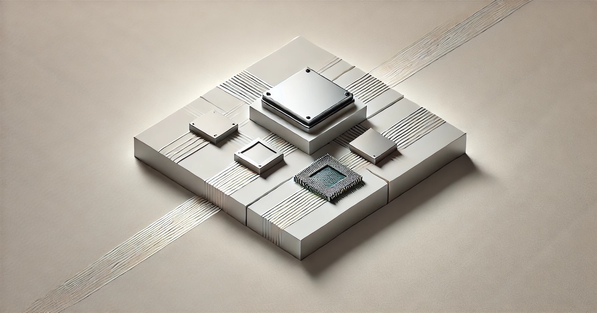
    Image Generated Using DALL-E


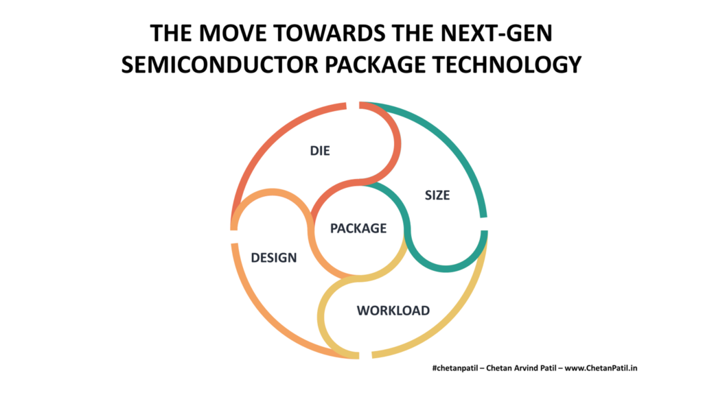
    Continuous Package-Level Scaling

    Moore’s Law, which predicted the doubling of transistors every two years, is slowing down due to atomic-scale limitations. The industry is adapting by shifting towards advanced packaging solutions that enable continued performance scaling without the need for extreme lithography advancements, such as EUV (extreme ultraviolet) lithography or multi-patterning techniques.

    These new methodologies are not just a shift, but a leap forward in semiconductor technology. They facilitate enhanced chip density, lower power consumption, and higher performance across various applications.

    Some of the key package-level scaling approaches include:

    • 2.5D and 3D Integration: Stacking chips vertically (3D ICs) or placing them side-by-side on an interposer (2.5D) increases transistor density, enhances bandwidth, and reduces interconnect delays. This approach benefits high-performance computing and AI applications that demand massive data throughput.
    • Heterogeneous Integration: Integrating diverse chiplets, logic, memory, RF, analog into a unified package enables optimized performance per function, minimizing power loss and latency while improving efficiency. This allows for tailored architectures that cater to specific workloads, reducing the need for monolithic designs.
    • Hybrid Bonding: A next-generation interconnect method that facilitates denser packaging by directly bonding dies at a molecular level, significantly improving performance and reducing power consumption. This approach also enhances signal integrity and minimizes the parasitic effects of traditional interconnects.
    • Advanced Thermal Management Solutions: As power densities increase, thermal challenges must be addressed through innovations like embedded microfluidic cooling, thermal interface materials, and optimized heat dissipation structures to maintain system reliability.
    • Photonic Integration: The convergence of electronic and photonic components within a package enables ultra-fast optical interconnects, reducing latency and power consumption for data-intensive applications such as AI, cloud computing, and high-speed networking.

    This evolution in packaging enhances system-level performance, optimizes power efficiency, and provides superior thermal management, which is critical for AI workloads, high-performance computing, and next-generation consumer electronics.


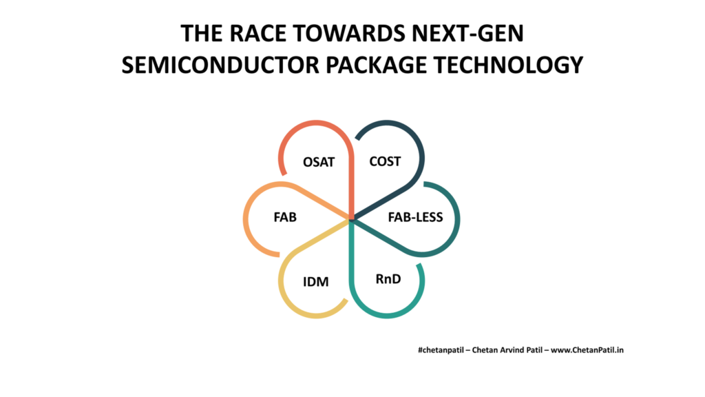
    Packaging Cost And Economic Feasibility

    While advanced packaging drives performance scaling, its adoption is increasingly fueled by cost considerations. Traditional monolithic scaling is becoming unsustainable due to rising fabrication costs, process complexity, and diminishing yield efficiency. The heavy reliance on EUV lithography and cutting-edge fabs demands massive capital investments, making continued node scaling economically impractical for many manufacturers.

    To mitigate these costs, the industry is shifting toward advanced packaging, which enables performance gains without aggressive transistor scaling. By integrating modular components and optimizing interconnect solutions at the package level, companies can enhance power efficiency, improve yield, minimize material waste, and extend the usability of mature process nodes, all while controlling manufacturing expenses.

    The following (few) advanced packaging techniques are enabling this transition by balancing performance with economic feasibility:

    • Chiplet-Based Design: Breaking down a large monolithic die into smaller functional chiplets reduces defect rates and improves yield.
    • Fan-Out Wafer-Level Packaging (FO-WLP): A cost-efficient alternative to traditional wire bonding, improving I/O density and electrical performance while reducing the package footprint.
    • Co-Packaged Optics (CPO): Reducing power consumption and improving data transmission speeds for high-performance computing applications.
    • Substrate-Less Packaging: Eliminating the need for an interposer or traditional substrate, which significantly reduces material and production costs.
    • Wafer-Level Chip Scale Packaging (WLCSP): Reducing manufacturing complexity by performing packaging steps at the wafer level, which lowers production costs and improves efficiency.

    These advanced packaging techniques offer varying trade-offs between cost, performance, and complexity. While some approaches, like chiplet-based design, balance efficiency, and scalability, others prioritize high performance at greater complexity, such as co-packaged optics.

    The table below highlights these distinctions, helping to evaluate cost-effective solutions for different semiconductor applications.

    Packaging TechniqueCost EfficiencyPerformanceComplexity
    Chiplet-Based DesignHighHighModerate
    Fan-Out Wafer-Level (FO-WLP)ModerateHighLow
    Co-Packaged Optics (CPO)ModerateVery HighHigh
    Substrate-Less PackagingVery HighModerateLow
    Wafer-Level Chip Scale (WLCSP)Very HighModerateLow


    Manufacturability Considerations In Advanced Packaging

    The shift to advanced semiconductor packaging demands significant investment in specialized equipment to support complex integration techniques. Hybrid bonding, wafer-level processing, and high-precision lithography require next-generation tools capable of nanoscale accuracy. Advanced metrology and inspection systems are essential to detect defects early and maintain high yields, making capital-intensive upgrades a necessity for semiconductor manufacturers.

    Material innovations are also critical in overcoming manufacturability challenges. New substrates, dielectrics, and thermal interface materials are required to enhance interconnect performance, power efficiency, and reliability. High-density redistribution layers (RDLs) and ultra-thin interposers are pushing the limits of traditional materials, requiring ongoing research and collaboration with material science experts.

    A skilled talent pool is even more essential to scale advanced packaging technologies. As manufacturing complexity increases, companies must invest in specialized workforce training for precision assembly, hybrid bonding techniques, and AI-driven quality control. Bridging the talent gap requires academic partnerships, internal training programs, and a shift in workforce development strategies to meet the evolving demands of semiconductor packaging.

    Finally, investment in infrastructure is critical to ensuring long-term manufacturability. Establishing localized packaging hubs reduces supply chain risks and enables tighter control over production processes. Governments and industry leaders are increasing funding for domestic packaging capabilities to secure technological leadership, reinforcing the strategic importance of advanced semiconductor packaging in the global market.


    Takeaway

    The semiconductor packaging shift has transcended its conventional role and emerged as a defining factor in the future of chip design and manufacturing. It is no longer just about protecting a chip, it is about unlocking new levels of performance, energy efficiency, and integration essential for the next generation of AI, computing, and high-speed connectivity.

    As traditional transistor scaling reaches its limits, the chip design’s ability to innovate depends heavily on the advancements in heterogeneous integration, 3D stacking, and high-bandwidth memory architectures.

    Companies that embrace these advanced packaging technologies will position themselves at the forefront of semiconductor progress, driving breakthroughs in areas ranging from mobile computing to AI supercomputing infrastructures. The combined impact of manufacturability enhancements, cost-effective design strategies, and material innovations will determine how effectively the industry can sustain growth while meeting the rising demands for performance and efficiency.

    With scaling, economic feasibility, AI-driven architecture, and supply chain resilience shaping the evolution of semiconductor packaging, the industry must recognize that packaging is no longer an afterthought. It is the foundation upon which the next wave of semiconductor breakthroughs will be built, ensuring sustained innovation and competitiveness in an increasingly complex technological landscape.


  • Why The Semiconductor Industry Is Speedily Adopting Advanced Packaging

    Why The Semiconductor Industry Is Speedily Adopting Advanced Packaging

    Image Generated Using Adobe Firefly


    Semiconductor packaging is one of the last steps in semiconductor manufacturing and a crucial one. Protecting the silicon die from physical, mechanical, and thermal damage is only possible with a packaging solution. Silicon package technologies are also vital in developing interfaces that enable new architectures, like chiplet based XPUs.

    Historically, ever since the first silicon, there have been efforts to accommodate new types of package technologies by adapting the requirements of the end application. It has been in line with Moore’s law.

    Lately, one such adoption is embracing the advanced packaging technique. It is a needed solution that enables the path towards the More-Than-Moore era.

    So, what does advanced packaging mean? In simple terms, advanced semiconductor packaging refers to assembly techniques developed to provide technical solutions that enable interconnections of multiple dies.


    Picture By Chetan Arvind Patil

    And why does the semiconductor industry need to adopt advanced packaging speedily? There are several reasons. Below are the few top ones:

    Performance:

    A single die and how much performance it can drive directly correlates to the physics of the semiconductor. Traditionally, it means the transistors and how fast they can shrink to double the number per the same area. Considering the ever-increasing demand for performance by the applications, it is slowly becoming impossible to cater to the advanced requirements (mainly for XPUs that are stretched to their limits by the AI applications). It is where advanced packaging comes into the picture and allows the integration of homogeneous and heterogeneous silicon die to create a more robust system of silicon chips. All of which leads to better performance.

    Functionality:

    Chiplet is the most talked about topic in the computing and silicon industry. The most vital aspect of chiplet is not the desegregation of the silicon die into multiple chiplets or the fabrication and testing of it, but the packaging aspect. It is valuable if the chiplets can get integrated without affecting their functionality. It is where the advanced packaging is applicable. The System-in-Package (SiP) solution is one such example of advanced packaging. It allows better integration of multiple dies and suits SoCs utilizing ultra-advanced nodes.

    Node:

    Advanced packaging provides the ability to keep utilizing the matured process nodes. It is to be done mainly through chiplets, which offer the ability to integrate the latest and matured nodes and then use advanced packaging to enable better node utilization, which means not having to rely on one specific technology node.

    Innovation:

    One of the most critical impacts of advanced packaging is to enable new silicon design. Whether by utilizing 2D, 2.5D, or 3D integration, advanced packaging provides an avenue to innovate that is not limited to die-level innovation. With advanced packaging, it has become possible to develop better integration techniques to overcome the limit of space-constrained die.

    While there are benefits to embracing advanced packaging solutions, it also comes with its challenges.

    The major challenge is for the semiconductor assembly vendors, who must invest the capital to develop facilities that can enable such advanced integrations and consistently develop process features to ensure the end cost is ROI-friendly.

    With Moore’s Law’s diminishing returns regarding cost and performance benefits. Advanced packaging is here to play a crucial role in continuing the evolution of semiconductor capabilities and meeting the demands of new-age computing systems.

    Advanced packaging addresses both technological challenges and market demands by allowing for improved performance, functionality, node utilization and driving innovation. Thus, it has become a solution that semiconductor assembly vendors are rushing to develop, and the foundries are getting into it.

    The next few years will likely see the most activity in this domain and can provide a new trajectory for the semiconductor assembly industry.


  • The Growing Influence Of Semiconductor Package On Scaling

    The Growing Influence Of Semiconductor Package On Scaling

    Photo by Christopher Bill on Unsplash


    Advancements in package technology are as vital as advancements in technology nodes. These two semiconductor solutions enable silicon products to work per the required specifications. Technology node innovation has occurred more rapidly than package technology. Given that now the technology node is going to hit the node wall, it is time for package technology to provide avenues to shape the future of next-gen silicon design and manufacturing.

    The semiconductor package has always been an integral part of semiconductor manufacturing. It has shaped and powered different silicon features and cost-optimized solutions for several decades. Semiconductor package technologies also ensure that the end-product can withstand harsh operating conditions by managing different thermal, chemical, physical and mechanical characteristics.

    Features: Package level scaling creates silicon area for new features.

    Cost: Cost optimization by leveraging the best of package level scaling.

    The focus on package technologies has further grown in recent years. The primary reason is the diminishing die-level scaling opportunities, which raises questions on how the next era of silicon devices will evolve in size, shape, feature, efficiency, and performance. The answer lies in the semiconductor package evolution.

    For the last decade, semiconductor package technology has consistently shown the ability to spread the die-level blocks across the different layers with the help of connections via industry-standard interfaces. It provides avenues to continue scaling for high-performance die blocks and thus deliver higher than ever capabilities.

    The impact of such solutions from the semiconductor packaging world is evident in heterogeneous architectures like chiplets, and the influence of such packaging qualities will grow in the coming years.


    Picture By Chetan Arvind Patil

    Scaling beyond a certain point, at the die level, is complex and error-prone. It is also getting costlier and time-consuming to keep enabling die-level optimization to package more devices for better features and performance and thus pushes the industry toward package-driven scaling features.

    The advanced package technology to enable scaling allows better yield. On top, the risk of introducing errors is far less than other scaling options.

    Yield: Package scaling enables higher yield for complex design.

    Application: Scaling die level features to package level creates new type of applications.

    Apart from the yield, taking advantage of new types of packaging solutions also provides routes to design and develop new applications. It is evident from the powerful and portable solutions package technology-driven chiplet has started to enable. Similarly, different types of flip-chip solutions will soon power next-gen applications that will be far more efficient than what is available in the market today.

    The influence and impact of package technology are only going to grow further, and it has already become a crucial pillar in enabling next-gen devices. Semiconductor companies which incorporate the best of both die and package level scaling will eventually be able to launch better products.


  • The Contest For Next-Gen Semiconductor Package Technology

    The Contest For Next-Gen Semiconductor Package Technology

    Photo by Ryan on Unsplash


    THE MOVE TOWARDS THE NEXT-GEN SEMICONDUCTOR PACKAGE TECHNOLOGY

    Packaging plays an important role in almost all the industry. From cars to rovers, packaging the product before shipping is vital. Doing so cost-effectively is critical to ensure the product cost is not affected.

    The same story is valid for the semiconductor industry, where the packaging technology ensures that the silicon die is protected from harsh mechanical to environmental conditions.

    In a nutshell, package technology in the semiconductor industry is geared towards providing the following features to the die area:

    Thermal: Ensure the heat is dissipated efficiently out of the die to avoid thermal runaway.

    Mechanical: To save silicon from any outside impact like vibration or stress.

    Connectivity: Enable a pathway for connecting the die to another system via a printed circuit board.

    Contamination: Protect the die are from contamination due to long-term usage.

    Today, there are numerous package technologies to choose from. Eventually, the decision to decide on the package type is based on both the technical and the business points.

    Give the advancement in the semiconductor design and ever-shrinking technology-node, it is becoming a challenge for semiconductor packaging solution providers to come up with innovative packaging solutions that are also low-cost. All this is pushing the need for next-gen – InFO, CoWoS, CoC, FCiP, PoP, and many more – package technology solutions.

    The push towards next-gen package technology is driven by several factors:

    Die: Semiconductor product development is moving towards More-Then-Moore solutions. This means several new die-based solutions and one of them is chiplets. Chiplets is IP driven design process, where different die come together to form the same system which earlier would have been a single die. Chiplets are proving to be effective both from a cost and yield perspective. To cater to such requirements, package technology solution providers (OSATs) have to keep their innovation team engaged, to ensure not only the packaging solution is at-par with chiplets requirement but are also low-cost due to the stiff competition.

    Design: One example of modern semiconductor design change is the heterogeneous architecture. It has provided ways to bring different types of XPU together. This also requires an efficient way to package by considering the thermal profiles of such complex and high-frequency devices.

    Size: The shrinking size is also adding to the need to be more innovative in package technology. Not all devices will be small and at the same time also not too big. OSAT is facing a challenge to cater to different markets and while doing so, have to ensure the type or size of the device is not a constraint.

    Workload: Emerging workloads are becoming complex year-on-year. These workloads running on the die continuously end up heating the system. To mitigate such issues, new materials and packaging solutions are required. This is also one reason that is pushing OSATs towards next-gen package technology.

    OSATs have to continuously provide solutions that cater to both the smaller and larger die areas. This has to be done in coordination with the design houses, to ensure that next-gen package technology meets all customer requirements.

    However, lately, OSATs are being pushed from all the corners and are getting beaten in their own game by FAB-LESS to FAB houses.


    Picture By Chetan Arvind Patil

    Picture By Chetan Arvind Patil

    THE RACE TOWARDS NEXT-GEN SEMICONDUCTOR PACKAGE TECHNOLOGY

    The semiconductor package technology is mostly enabled by the OSATs. IDMs also play a crucial role. However, given the rise of the semiconductor packaging and testing business, OSATs are facing stiff competition from FAB and FAB-LESS companies too.

    This is leading to both positive and negative impact on all types of semiconductor companies:

    OSAT: The primary focus and strength of the OSATs have been the testing and packaging solutions. With growing competition from FAB on the packaging solutions is certainly putting OSAT in a position to not only innovate on the testing to packaging arena but also how to expand the business beyond traditional OSAT services. This certainly diverts the focus of OSATs, as it is more difficult to move towards FAB or FAB-LESS business while also catering to the same customer type.

    FAB: FABs all over the world have the biggest advantage due to the availability of high-tech and research facilities that can aid the innovation of next-gen package technology. This is why TSMC and Samsung have been at the forefront of next-gen packaging solutions. At the same time, FABs are also diversifying and entering the OSAT business with a strong packaging portfolio. 

    IDM: IDM has always enjoyed the best of both world. Intel already has many homegrown packaging solutions for its need, apart from the ability to fabricate, test and assembly in-house. The innovation in the design space is only benefitting IDMs as they can foresee and quickly adapt their business by pushing towards the required semiconductor packaging research and development activity, and quickly turn research into production-worthy solutions.

    FAB-LESS: While, majority of the FAB-LESS companies only focus on the design side. The need to have a packaging solution that can cater to their designs is also pushing FAB-LESS to continuously invest time and money in the packaging technology.

    Eventually, packaging solution for semiconductor products is driven by cost optimization. The innovative and low-cost packaging solution catering to the next-gen design will win the race. However, to do so massive research and development activity is required. Which certainly demands high CapEx.

    To balance the complexity and high CapEx, packaging solution providers (OSATs mainly) will have to be more innovative to ensure the next-gen solution is business-friendly.

    The race towards next-gen semiconductor package technology is certainly heating up, however, it is also an opportunity to innovate and create a new market for the emerging solutions.