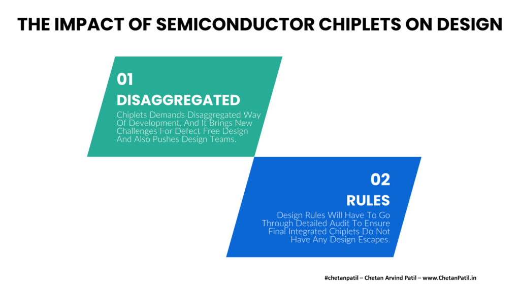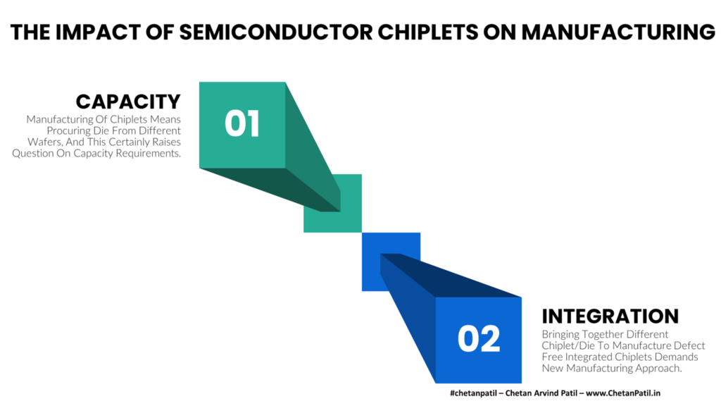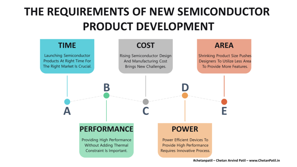
Image Generated Using 4o
What Is Semiconductor Productization Cycle Time?
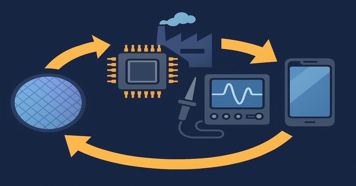
Semiconductor productization cycle time refers to the total duration required to transform a completed chip design into a fully qualified, production-ready product. It begins after the design is taped out and ends when the product is released to high-volume manufacturing with acceptable yield, quality, and system-level reliability. This period involves intensive cross-functional collaboration across silicon engineering, packaging, test development, validation, reliability, and supply chain.
The cycle is not a single step but a structured series of technical handoffs, optimizations, and problem-solving phases. Each contributes to overall time-to-market and has a direct impact on cost, quality, and revenue generation.
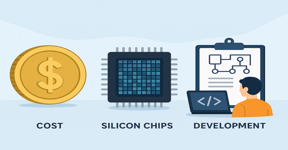
The key components of the productization cycle include:
- Tapeout to first silicon readiness
- Initial bring up and functional debug
- ATE test program development and correlation
- Package and assembly qualification
- Reliability and standards-based qualification testing
- Yield analysis and production ramp
- Customer validation and system integration feedback
Depending on the complexity of the product and the target market, this cycle can range from six months to over a year. Shortening the cycle without compromising quality is often a strategic priority, especially in competitive or regulated markets.
In the long-term, managing this time effectively is what differentiates strong product execution from delayed or over-budget programs.
Typical Timeline Of The Productization Cycle
The productization cycle consists of several tightly coupled stages. Each stage has its own objectives, deliverables, and potential bottlenecks. While exact timelines vary depending on product complexity, market segment, and technology node, the typical range for a complete cycle is six to twelve months.
The timeline below outlines each primary phase, its expected duration, and the core activities associated with it.
| Stage | Estimated Duration | Key Activities |
|---|---|---|
| First Silicon Readiness | 4 to 6 weeks | Tapeout to wafer delivery, packaging for evaluation |
| Silicon Bringup | 2 to 6 weeks | Basic functionality, register access, debug loops |
| Test Program Development | 8 to 12 weeks | ATE pattern creation, DFT validation, test coverage |
| Package Assembly | 4 to 6 weeks | Substrate readiness, thermal and form factor checks |
| Reliability Qualification | 6 to 12 weeks | HTOL, HAST, Temp Cycle, ESD, latch-up tests |
| Yield Ramp and Optimization | 8 to 16 weeks | Process tuning, guardband validation, corner lots |
| Customer Validation | 4 to 8 weeks | Application-level tests, system integration |
In many cases, some stages run in parallel to save time. For example, reliability testing and test program optimization may proceed concurrently after bringup. However, any failure in these parallel flows can lead to rework, which resets the clock for the affected stage.
Thus, efficient productization requires not only strong technical execution but also program-level coordination to ensure each stage feeds smoothly into the next. Such a structure becomes even more critical when managing tape-outs across multiple products or process nodes.
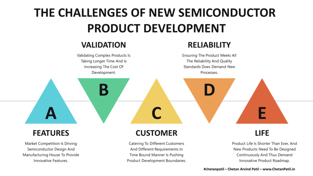
What Drives Productization Delays
Delays in the productization cycle are common due to the technical complexity and cross-functional nature of semiconductor development. Common causes of delay include:
- Incomplete Pre-Silicon Validation: Simulation fails to capture real-world corner cases that emerge only during bring-up
- DFT and ATE Mismatch: Poor alignment between design-for-test features and test platform implementation slows test development
- Packaging Issues: Packages may face late-stage problems with thermal, mechanical, or signal integrity
- Qualification Failures: Reliability tests, such as HTOL or HAST, can fail, requiring debugging and retesting cycles
- Yield Instability: Low or inconsistent yield across corners demands additional tuning and analysis
- System-Level Gaps: Customer-side failures frequently result in late changes to silicon or test programs
Even with detailed planning, issues often emerge from immature designs, process variability, and misaligned engineering handoffs.
How Cycle Time Impacts Cost
The productization cycle time has a direct impact on development costs. Each added week increases engineering effort, lab usage, and the need for additional silicon or packaging builds.
These costs rise rapidly, especially for complex System-on-Chip (SoC) designs or high-reliability products. These longer cycles also stretch budgets and delay production, reducing the time available to recover investment.
Delays also create opportunity costs. Missing key market windows or customer ramps can result in lost sales opportunities, lower selling prices, or even canceled projects.
Underutilized equipment and late delivery in regulated markets may also trigger penalties. Managing cycle time effectively is essential for both technical execution and business success.
Strategies To Optimize Productization Time
Reducing productization cycle time requires more than just faster execution. It requires a structured, cross-functional approach that addresses bottlenecks, enhances handoff efficiency, and anticipates familiar sources of delay. Leading semiconductor companies treat productization as a tightly managed engineering flow, where technical readiness is synchronized with program planning and customer engagement. By front-loading risk and parallelizing key activities, teams can compress timelines without sacrificing quality or reliability.
Below are the strategies to optimize productization time include:
| Strategy | Description |
|---|---|
| Early Test Development | Begin ATE pattern development and validation before first silicon using virtual test setups and simulations. |
| First-Time-Right Design Culture | Emphasize high-quality closure throughout the design cycle using linting, static checks, and sign-off tools to reduce post-silicon issues. |
| Cross-Functional Ownership | Assign dedicated ownership early in the cycle to coordinate activities across design, test, validation, packaging, and customer engagement. |
| Parallel Qualification and Debug | Run reliability testing and test debug in parallel with early silicon to minimize serial dependencies. |
| Unified Pre and Post-Silicon Flow | Align pre-silicon simulation environments with production test platforms to improve correlation and reduce transition time. |
| Strong Data Infrastructure | Use analytics tools for yield, failure analysis, and traceability to support faster debugging and feedback. |
| Supplier and Customer Integration | Engage OSATs, substrate vendors, and customers early to align requirements, timelines, and failure response plans. |
When these strategies are executed with discipline and data-driven feedback loops, teams can reduce cycle time significantly while improving first-pass success rates.
Eventually, the result is not only faster product release but also greater cost control and more substantial customer confidence.