Category: SERVICE

  • The Implications Of Semiconductor FAT Outsourcing

    The Implications Of Semiconductor FAT Outsourcing

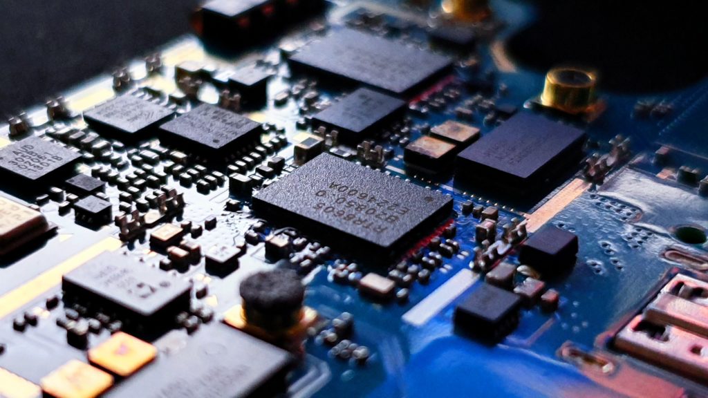
    Photo by Yogesh Phuyal on Unsplash


    THE IMPACT OF SEMICONDUCTOR FAT OUTSOURCING

    The process of developing a semiconductor product requires several business and technical components to work together. Depending upon the business model of the semiconductor company, these development activities (mainly design and manufacturing) can be insourced or outsourced.

    The technical aspects of semiconductor product development are often insourced and developed in-house. Doing so requires investing in teams to drive research and development activities. The outcome of these efforts is patents and intellectual property, which in turn allows the development of more advanced products and thus provides an edge over other semiconductor companies. However, the manufacturing part of the semiconductor can be executed in two ways: in-house or outsourced, and the final decision is based on the business requirements and planning.

    The business component of semiconductor product development mainly decides on how to develop the product after the design stage: semiconductor manufacturing. In the last few decades, semiconductor manufacturing has become more outsourced than insourced, and the major driving factor for this is cost optimization apart from resource balance.

    The outsourcing model in semiconductor manufacturing is applied to three specific domains:

    Fabrication: Pure-Play FABs are hired to fabricate wafers.

    Assembly: Vendors who provide different types of silicon packaging services.

    Test: Semiconductor houses that are capable of providing resources to test wafers and packaged products.

    FAT – Fabrication, Assembly, And Test – outsourcing has increased mainly due to FAB-LESS growth. However, as the number of companies without in-house semiconductor manufacturing grows, the dependence on external vendors increases too. Over the years, the process and business model of semiconductor FAT outsourcing have to lead to both pros and cons.

    Time: Every semiconductor design company wants to see their product go through semiconductor FAT in the shortest time possible. In reality, it is dependent on the vendor who is hired for the semiconductor FAT. If there is no capacity or resource constraint then the manufacturing time is fast, otherwise, the manufacturing process can take a lot of time, which is what is happening during the semiconductor shortage.

    Reliance: As the semiconductor FAT outsourcing business grows, the reliance on external vendors is increasing year on year. This makes planning an important part of the semiconductor product development as any slip on the vendor side can hurt the design houses and their business. In case of any hiccups and difficulties, it is not easy to switch the outsourced vendor overnight, and this process makes it critical to capture and plan for countermeasures.

    Cost: Not investing in internal manufacturing capacity can certainly reduce the CapEx and allows semiconductor companies to focus on building next-gen products. In the long run, semiconductor FAT outsourcing can provide several cost benefits. However, care should be taken for scenarios when external resources run out of capacity due to demand, and it turns starts increasing the cost of outsourcing.

    Features: In the end, all semiconductor design houses are providing features. These features are in form of packaged products but internally several sub-features are driving the system. Some critical features are dependent on the outsourcing vendors who are capable of fabricating as per the requirement (technology-node for example) and then can also package parts as per package technology. This also means that majority of the design features are also driven by well equipped the semiconductor FAT providers are.

    Resource: One of the most positive impacts of semiconductor FAT outsourcing is resource allocation. By focusing on design and then letting external vendors manufacture, enables semiconductor companies to focus on future roadmap while external vendors bring today’s product to reality.

    Semiconductor FAT outsourcing is not new and has been around for decades. The future of semiconductor outsourcing looks bright mainly due to the growing market and it will certainly make semiconductor design (mainly FAT less) houses more dependent on FAT outsourcing than ever, but the semiconductor shortage and impact it had on the industry is going to make certain specific changes in the future of semiconductor FAT outsourcing.


    THE FUTURE OF SEMICONDUCTOR FAT OUTSOURCING

    Recent development in the semiconductor industry is now questioning the worldwide semiconductor manufacturing capacity. From the technology point of view, it is difficult to build capacity overnight and this makes the manufacturing process far more critical than few other stages in the product development phase.

    Semiconductor dependent end-companies/customers (and even governments) have realized the role played by the semiconductor manufacturing process. On top of that, the companies and governments are also realizing that it takes time, effort, and a large amount of investment to build a basic semiconductor manufacturing infrastructure.

    All these new learnings are certainly pushing the future of semiconductor FAT outsourcing. In the long term, all the push might bring more market for the semiconductor outsourcing business.

    Diverse: Today, there are specific regions that are dominating the semiconductor FAT outsourcing business. The experience gained out of the semiconductor shortages is pointing to the fact that there is a need for a far more diverse manufacturing supply chain. Whether this is by building more capacity or by upgrading existing ones, the end result will be more diverse (spread across different countries) than it is today.

    Balance: Hiring external vendors for FAT is inevitable in many cases. Care must be taken by ensuring that there is no growing dependence on external vendors. This means the semiconductor companies should always have some percentage of internal capacity, but that requires CapEx, resources, and planning. In the end, it is not a good strategy to rely on external vendors for all semiconductor manufacturing needs and that is why it is becoming critical to balance internal manufacturing with external.

    Consolidation: There are different types of semiconductor FAT outsourcing options. Some are giant vendors who hold more than 40% of the market and then several smaller vendors also play a crucial role. As the semiconductor industry comes out of the semiconductor shortage issues, there will be more activity of manufacturing consolidation wherein smaller vendors will merge to bring investment for new capacity. This consolidation might also be driven by semiconductor companies (design-focused) acquiring manufacturing assets.

    Joint Ventures: Joint Ventures (JV) is another future roadmap that semiconductor FAT outsourcing will follow. This might see different FAB and OSAT opting for JVs with design houses. The probability of JVs happening at a very high rate is low, but this is certainly going to be the case for companies looking to enter the semiconductor manufacturing arena.

    Catch-Up: Semiconductor FAT outsourcing capacity crunch is going to drive new capacity along with up-gradation of existing ones. However, the majority of this new capacity might also come from regions and countries which never had any experience in the FAT outsourcing business. Governments worldwide are providing incentives to set up new FAB and OSAT capacity, and this will allow respective countries to catch up with the other FAT markets/regions.

    Ultimately the semiconductor manufacturing is going to be driven heavily by the FAT outsourcing model, and there is no harm in it. It is upon the semiconductor FAT less companies to understand their market and then accordingly invest either in the internal manufacturing capacity or the external ones.

    In the end, the semiconductor FAT outsourcing is going to keep rising as the semiconductor market grows.
  • The Need For Semiconductor As A Service

    The Need For Semiconductor As A Service

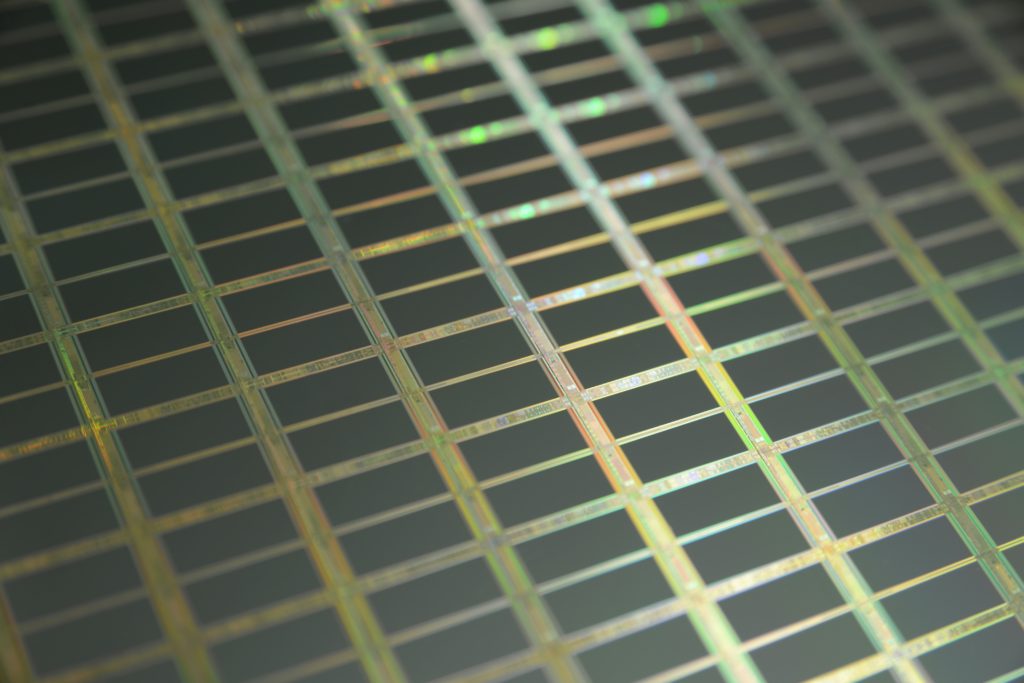
    Photo by Laura Ockel on Unsplash


    THE SEMICONDUCTOR AS A SERVICE

    The software industry has adapted to the demand of business and consumers by changing the licensing and product delivery model over the last three decades. The post-1990 saw standalone one-time fee-based software with no incremental feature updates except security-related and termed as the pay and use model. Then post-2000, with the proliferation of the internet, the software license model moved to pay over month/year and also came with features and security updates. The software industry termed it as Software-As-A-Service Model. Post-2010, the software industry adapted to the changing business and applied the licensing model from software to platform, which came not only with features and security updates for the software itself but also the platform the software will run on. It has allowed software developers to provide more over the top services.

    In comparison to the software industry, the hardware industry (mainly the semiconductor industry) has not adopted the product delivery model. It has been constant and driven by build and ship, with no ability to provide new hardware features on the go. If there are security flaws in the hardware, then those are suppressed by an Over-The-Air (OTA) update. Consumer and business buying the piece of silicon get locked in with the product. It is also not easy to provide new features at the silicon level. On top, the majority of the products shipped by the semiconductor industry end up getting used differently based on the hardware company’s need. 

    The semiconductor products (from CPUs to NPUs to GPUs to ASICs to FPGAs to DSPs to Mixed/Analog/Digital devices) have a long design and manufacturing cycle. It also means a long-term vision of the future market needs and then aligning the investment in the design to the manufacturing process accordingly. As per the market demand, semiconductor products need to be more adaptable with in-built features that are more relevant a few years down the line and can be activated post-production.

    Semiconductor-As-A-Service Is Possible Today Than Ever Due To The Shrinking Transistor Size That Allows More Silicon Features To Be Built-In Today For The Future Needs.

    The approximate life of a smartphone is anywhere between three to five years. However, the majority of companies stop providing critical software updates that make the smartphones redundant. The launch of new smartphones with new silicon and software grabs consumer’s attention and they end up buying a new smartphone with the latest silicon features.

    Imagine, having adaptable silicon with features built-in that can be unlocked a few years later and thus making the hardware as new as the software? Either vendors or consumers can decide which silicon features should be activated and how it helps the device performance. Such a process will allow the semiconductor industry to deliver silicon services under Semiconductor-As-A-Service model.

    Semiconductor-As-A-Service – A product delivery business model for the semiconductor industry which allows silicon design and manufacturing with in-built silicon features that can be unlocked in the future as the market demand and software requirements align. For example – More graphics for new gaming applications. These silicon features can be enabled with the help of software updates and require a subscription or one-time payment license. The list of features can be endless, from more cache memory to DRAM memory to extra processing cores to additional GPU for gaming applications to secondary cellular (perhaps 6G) antenna. The shrinking transistor size and growth of heterogeneous integration as a More-Than-Moore (MTM) solution makes such features in silicon possible. Silicon area with extra features can reside inside the smartphone launched in 2020 as an inbuilt hidden feature with the option to enable in 2022 as long as consumers are willing to pay. Such service can also be bundled with software features wherein the smartphone manufacturers can tie the new feature like extra memory or storage.


    Picture By Chetan Arvind Patil

    THE PROCESS OF SEMICONDUCTOR AS A SERVICE

    Semiconductor-As-A-Service implementation can unlock a plethora of opportunities not only for the semiconductor industry but also for the software industry. However, implementing Semiconductor-As-A-Service requires a specific process to be followed from designing to manufacturing. It also requires the semiconductor industry to take risks by providing advanced technology node use today rather than a few years down. Using advanced technology is the key to fitting more silicon features that can be unlocked post-production as it allows more silicon in the smallest possible area as this helps in providing more features at the transistor level.

    Semiconductor-As-A-Service Process:

    Identify Future Software Needs – These software features should be those that become bottlenecks for consumers. It can be from understanding whether the consumers will need more memory than the product has been shipped with so that with the growing data-driven application enabling an extra memory at the silicon level can cater to the software demand. The same goes for CPUs and GPUs for processing power.

    Design Silicon With In-Built Hidden Features – Post identification of future software needs, packing the silicon with features that get unlocked in the future. The majority of these features will reside inside the System-On-A-Chip (SoC), as the active components are the ones that can provide more benefits of service-based features than passive components. Usage of advanced technology node is key to enabling such silicon level features.

    Ability To Enable The In-Built Hidden Silicon Features – Incorporating the in-built hidden silicon feature requires not only designing it with secure memory to store keys to activate features but also requires a secure manufacturing process. The secure way of design and manufacturing ensures that there are no security flaws that can be exploited by hackers.

    Innovative Manufacturing And Packaging – The critical piece of the Semiconductor-As-A-Service process is to ensure that the manufacturing flow and the packaging technology use advanced techniques to consider the effects when more silicon area is activated. Activating new features (more memory or processing capability) can have significant power and thermal effect.

    Product Cost: Planting more silicon with the expectation that it will get used in the future under a pay-as-use service is a business risk. It is vital to price such products so that the design and manufacturing costs invested gets recovered even when in-built hidden features do not get utilized.

    Above are the five key process steps that lay the foundation of Semiconductor-As-A-Service. It has the potential to make the silicon more adaptive. It will require massive research and development before the industry can use it as a real-world solution.


    Picture By Chetan Arvind Patil

    THE NEAR-TERM IMPACT OF SEMICONDUCTOR AS A SERVICE

    If Semiconductor-As-A-Service is implemented and widely used, then it has the potential to transform the computing industry.

    The ability to enable an extra layer of processing power on the go provides a new way to process data. With 3.5 billion 5G subscribers by 2026, the data consumption will skyrocket, and having silicon with in-built hidden features to cater to such high processing and memory demand will take computing to another level. Semiconductor-As-A-Service can also enable date centers and OEMs vendors with avenues to save cost and increase revenue by providing silicon level services.

    Semiconductor-As-A-Service Provides Avenues To Put Future Silicon Technology In Today’s Silicon Area

    FABs, FAB-LESS, IDMs, OSATs, and ATMPs will be able to use technology designed for future silicon today. It will help them understand its impact and usage before launching future silicon technology on a large scale. The semiconductor industry has already started embracing chiplets and heterogeneous computing. These two semiconductor and computing techniques can provide a perfect starting point where more silicon can be incorporated to use it in the future.

    IP based semiconductor business is going to benefit the most as it will allow designers to incorporate more features that can be locked and unlocked as per the need. FAB-LESS companies will make more business by providing vital features as-a-service.

    Semiconductor-As-A-Service also means every device out in the market is different than others as silicon features can be enabled and disabled to the consumer’s liking.