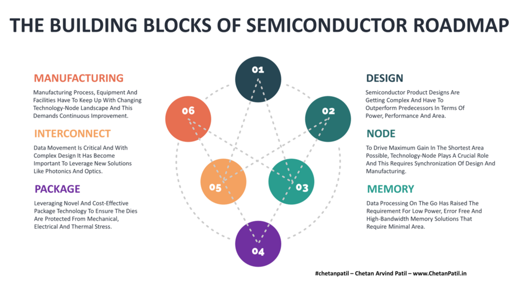
The semiconductor industry is no longer defined solely by the race for smaller nodes, such as 7nm, 5nm, or 3nm. Instead, its true strength lies in the versatility of specialized process flavors within each node.
These process variations are engineered to cater to specific applications, whether they are low-power, high-performance for data centers, or specialized functionalities like RF communication, sensor integration, or embedded memory.
Process flavors enable customization and optimization, driving innovation across industries and allowing fabs to maximize efficiency and adaptability.
Process Flavor Vs Process Nodes
Instead of universally pursuing node minimization, process flavors prioritize customization, tailoring fabrication processes to meet the diverse requirements of specific applications.
Node: A process node refers to the semiconductor manufacturing generation, measured by the smallest feature size (e.g., 7nm, 5nm). It broadly represents improvements in transistor density, performance, and power efficiency. Smaller nodes enable more transistors per chip, increasing computational power and efficiency. As nodes approach physical limits, advancements become more complex and costly.
Flavor: A process flavor is a specialized variation within the same node, optimized for specific applications like low power, high performance, RF, or embedded memory. For example, a 28nm node may offer flavors like LP (low power) or HP (high performance), enabling fabs to meet diverse market needs.
Why Process Flavors Are Essential Across Industries
Process flavors have become essential in enabling the semiconductor industry to cater to diverse markets and technological needs effectively. Unlike the one-size-fits-all philosophy of node shrinking, process flavors allow manufacturers to customize solutions for distinct application areas.
For instance, in the automotive industry, high-reliability and high-temperature process flavors are crucial for ensuring the safety and durability of in-vehicle systems. Similarly, for consumer electronics, low-power process flavors optimize battery life in mobile devices, while RF process flavors enable seamless wireless communication.
This adaptability also extends to high-performance computing, where process flavors are optimized for maximum computational throughput, and wearables, where ultra-low-power flavors enhance energy efficiency. By offering a variety of process flavors at the same node, fabs can serve a broader range of applications without the need for separate manufacturing lines.
This improves cost efficiency and resource utilization and drives innovation in industries where traditional node-based approaches may fall short. Process flavors are thus at the heart of creating tailored semiconductor solutions, pushing the boundaries of what chips can achieve in every domain.
How Are Process Flavors Classified
Process flavors are classified based on their optimization objectives, target applications, and specific design requirements. This classification enables fabs to offer tailored solutions for diverse industry needs while optimizing the performance, power efficiency, cost, and functionality of semiconductor devices.
Below is an example category used to classify process flavors:
Process Node
Process Flavor
3nm
GAA (Gate-All-Around) for HPC
Low-Power FinFET for mobile devices
5nm
High-Performance FinFET for AI/ML
Low-Power FinFET for IoT
7nm
HPC-Optimized FinFET for AI accelerators
Low-Power FinFET for edge devices
10nm
Embedded DRAM (eDRAM) for storage
Performance CMOS for networking
28nm
Low-Power (LP) for mobile
High-Performance (HP) for computing
RF SOI for communication
40nm
High-Voltage CMOS for industrial
Low-Cost CMOS for automotive
Take Away
Process flavors are designed and classified to meet the unique needs of different industries, balancing performance, power efficiency, cost, and functionality. This allows semiconductor fabs to create solutions tailored to specific markets.
The industry can then adapt to diverse challenges by offering specialized options, such as the demand for faster processors, energy-efficient devices, and advanced features like RF communication and embedded memory.
This flexibility is essential in today’s computing world, where application evolves quickly and industries have unique requirements. Process flavors enable fabs to innovate for variety of applications from high-performance to smartphones.
In short, classifying process flavors ensures the semiconductor customers and fabs both can meet the needs of different markets, stay flexible, and continue driving innovation that powers our modern world.
The semiconductor industry has long been dedicated to achieving exceptional performance, efficiency, and cost-effectiveness, primarily by advancing smaller process nodes. However, the increasing physical and economic challenges of further node shrinking have prompted a strategic shift in focus.
This exciting shift, known as ‘process flavor, ‘is not just a change in direction but a potential game-changer for the semiconductor industry. It involves the development of customized process technologies that are finely tuned for specific applications, marking a significant departure from the previous node-centric approach. With its potential to completely transform the industry, this innovative approach holds great promise for the future.
Process Flavor Vs Process Nodes
In the traditional semiconductor landscape, the drive towards smaller process nodes has been the hallmark of progress, symbolizing advancements in miniaturization, speed, and power efficiency. The smaller the node, the more transistors can be packed onto a chip, leading to higher performance and lower power consumption. This relentless pursuit, governed by Moore’s Law, has propelled the industry through remarkable technological milestones, with current leading-edge nodes reaching 3nm and 2nm. However, pursuing smaller nodes is becoming increasingly fraught with challenges, including astronomical RnD costs, manufacturing complexities, and diminishing returns in performance and efficiency gains.
Conversely, process flavor ushers in a new era in semiconductor manufacturing. Instead of fixating on the most minor possible node, process flavor advocates for customizing process technologies to meet specific application needs. This approach acknowledges that different applications, from high-performance computing to low-power devices, have unique requirements that can only be met through specialized process optimizations rather than a universal node shrinkage. By tailoring processes to specific use cases, manufacturers can achieve significant improvements in performance, cost efficiency, and energy consumption, all while mitigating the mounting challenges associated with node scaling. This strategy enhances technological versatility and market responsiveness and fosters innovation in areas where traditional node-focused approaches may need to be more effective.
As the semiconductor industry evolves, manufacturers’ strategies are diversifying to meet a variety of technological and market demands. Traditionally, the focus has been on shrinking process nodes to achieve higher performance and efficiency.
However, the emerging strategy of process flavor, which involves tailoring semiconductor manufacturing processes to specific application requirements, is gaining traction. This comparison table highlights the key differences between process flavor and process nodes, illustrating how each approach impacts various aspects of semiconductor technology and manufacturing.
Feature
Process Flavor
Process Node
Definition
Customizing semiconductor processes for specific applications
Generally more cost-effective for targeted applications
Higher RnD and manufacturing costs due to complexity
Performance
Tailored performance for specific use cases (e.g., power efficiency, speed)
Higher performance potential through increased transistor density
Complexity
Increased design and manufacturing complexity due to customization
High complexity due to advanced lithography and fabrication techniques
Market Adaptability
Flexible and responsive to diverse market needs
Primarily driven by leading-edge markets and high-volume applications
Sustainability
Can optimize for energy efficiency and resource usage
High energy consumption and environmental impact at advanced nodes
RnD Investment
Focused on developing multiple specialized processes
Large investments required for each new node generation
Technological Challenges
Balancing customization with manufacturing feasibility
Physical and economic limits of silicon technology
Innovation
Encourages innovation in diverse application areas
Innovation primarily in lithography and transistor scaling
Adopting a process flavor approach allows semiconductor manufacturers to tailor their technologies to meet the diverse demands of various applications, ranging from high-performance computing to energy-efficient devices. This strategy can lead to more sustainable practices and potentially lower development costs, as it avoids the escalating complexities associated with further node shrinking.
While process nodes have propelled significant technological progress, the transition to process flavor signifies a nuanced comprehension of market demands and technological capabilities. By harmonizing these two approaches, manufacturers can sustain innovation and deliver optimized solutions that precisely match the requirements of diverse applications, thereby fortifying the semiconductor industry’s resilience and adaptability.
Take Away
As the semiconductor industry navigates the challenges of advancing node shrinking, focusing on process flavor offers a balanced and strategic approach. By optimizing manufacturing processes for specific applications, semiconductor manufacturers can achieve significant performance and efficiency gains while managing costs and complexity. This shift addresses the limitations of pursuing ever-smaller nodes and paves the way for more sustainable and diversified technological advancements in the semiconductor industry.
The semiconductor node is the most vital technical topic in the semiconductor industry. Technology node forms the basis for developing different types of silicon products. Over the last decade, top semiconductor manufacturers have invested a lot of time and capital to bring new semiconductor technology nodes.
Such push is due to two critical aspects. The first one is technical, as it focuses on bringing new advanced solutions to the market. The second one is more business-oriented, where the manufacturers bring new capacity to manage future demand.
Focus: Semiconductor Companies Consistently Focus On New Node Technology.
Planning: Semiconductor Node Development Demands Capacity Planning.
Eventually, the demand for a specific technology node is due to the market and application use cases. However, even with all the available data about how the consumer market will grow, there is still a gap between the type of technology node capacity.
This gap is due to the focus on bringing capacity for the matured technology. It is a logical step given the need to cater to different system applications that still rely on such technology nodes. On the other side, to ensure future demand for advanced nodes is met, there needs to be a balance in semiconductor fabrication capacity.
To bring the balance in semiconductor technology nodes, not only manufacturers should plan and invest, but public bodies also need to provide the required incentives and policies impetus. Several of the advanced semiconductor node FABs are only possible due to support from government bodies.
The current view of semiconductor FAB type clearly shows that the 200nm wafer FABs are dominant. Within 200nm FABs, matured technology capacity share is more than 30-40%. It is due to the market requirements and the need to support legacy products.
Balance: A Perfect Balance Of Technical And Business Requirements Is Needed.
Application: Semiconductor Application And Use Cases Are Changing The Node Roadmap.
However, long term, the share should reduce from matured to advanced technology, mainly to ensure the next-gen applications can use the features provided by the advanced technology node.
As the focus on building better and larger semiconductor FABs increases, the crucial part will be to plan the capacity concerning the node type. So that it not only benefits future applications but also pushes the semiconductor industry towards shortage resiliency.
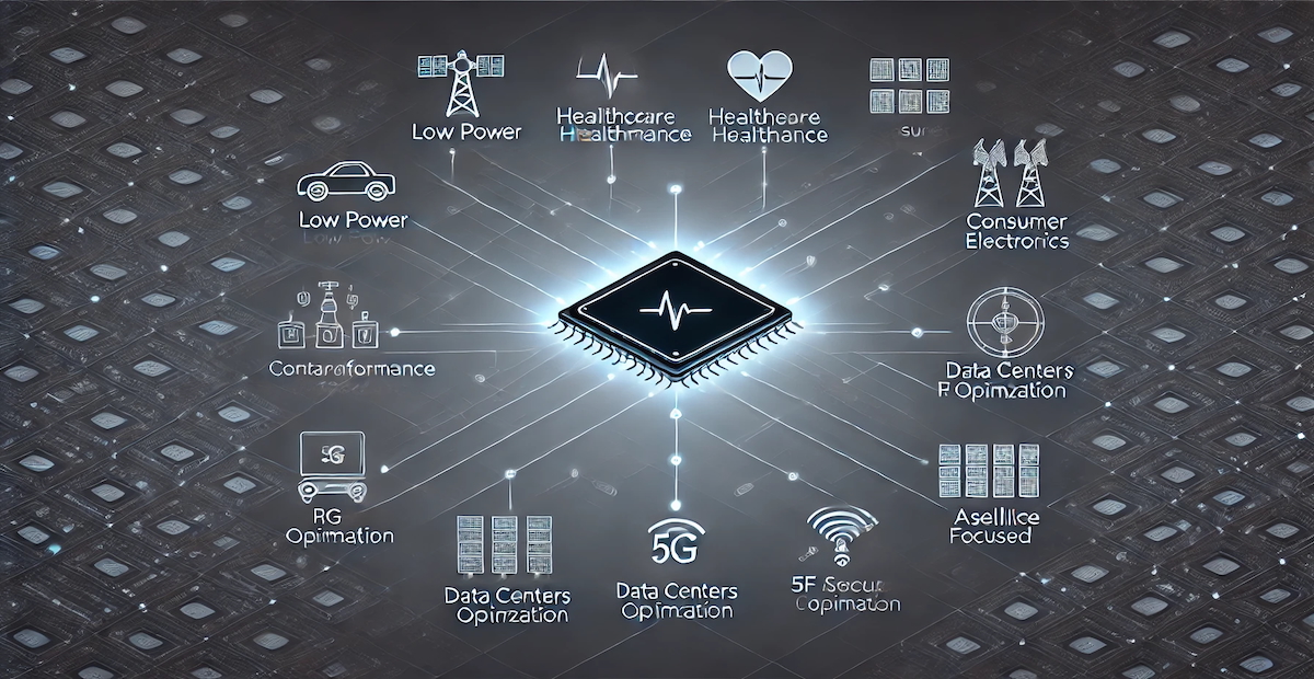
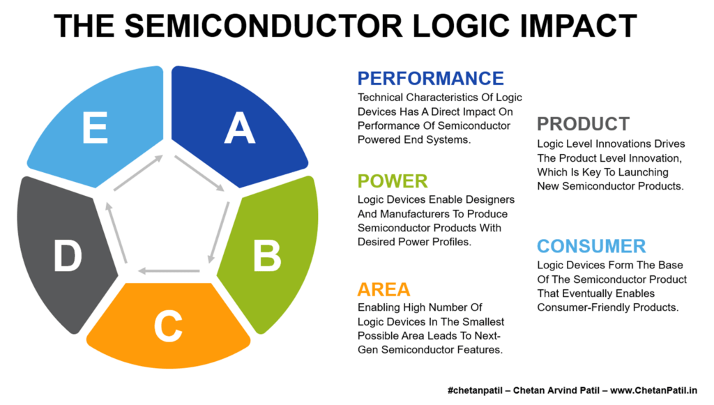
Logic devices (FETs) are the building blocks of semiconductor products. Today’s silicon chip can easily have billions of these logic devices. It is also in line with Moore’s law, and today’s semiconductor technology allows the possibility of packing more logic devices without impacting the total silicon area.
Semiconductor equipment and other semiconductor technologies have also played a key role in achieving the goal of fabricating innovative logic devices. Apart from this, both academia and industry have consistently provided novel ways to design logic devices for the future requirements of semiconductor products.
The impact of these logic devices on the overall semiconductor product-driven system is high and ranges from the technical to the business aspect. It is the primary reason the semiconductor design and manufacturing houses are always coming up with techniques to improve the efficiency of logic devices.
Performance: Logic devices directly impact the performance of the overall semiconductor products. The reason is the faster turn on/off time. To power performance-oriented silicon chips, underlying logic devices need to have the required characteristics that enable high performance. It is also the primary reason the industry is adopting next-gen FET devices.
Power:Several systems that do not require high-performing logic devices. Instead, they need a device that can work over different power profiles. It is usually the requirement of low-power semiconductor products. It is also where logic devices need to have smaller power footprints come into the picture and have been around for decades.
Area: The need to pack more logic devices will keep increasing due to the demand for faster processing. It is where logic devices play a crucial part and often have to evolve (technical features at the gate level) to cater to the next-gen processing demand while having minimal impact on the silicon area.
As the semiconductor industry moves towards the era where silicon chips might easily have trillions of logic devices, the need for next-gen logic devices that have minimal impact on the cost and time will grow too.
Logic devices also drive the business aspect of semiconductor products. It is in the form of products that get launched and what type of new features these products will have.
Product: New semiconductor products need to be at par with the predecessor products. It is only possible if the underlying semiconductor technology evolves as per the changing requirements. It requires advanced logic devices.
Customer:Consumer-friendly products require a good balance of internal architecture capabilities. It often ranges from response time to battery life. These two features are driven by the building blocks of the semiconductor products i.e. logic devices.
More than the semiconductor design, semiconductor manufacturing needs to invest more time and money to enable new logic devices. The majority of the investment eventually provides the next-gen solutions to the semiconductor industry at large. FinFET is one such example, which originated due to the cross-industry and academia efforts.
As the need to pack more transistors without affecting the time, area, and cost increases, the investment towards the research and development activities of the logic devices will have to increase too.
In the end, the semiconductor design and manufacturing companies will keep innovating to prepare themselves for the decades to come, and academia will also play a crucial role in promoting next-gen logic devices.
THE COMPLEXITY OF SINGLE-TECHNOLOGY-NODE ARCHITECTURE
To ensure high-speed processing, one active component in a computer system – the Central Processing Unit (CPU) – has seen numerous technological advancements.
The CPU advancements have been distributed equally on the design and the manufacturing aspect of the semiconductor development process, both driven by Moore’s law.
Design: During the pre-internet era, the CPU used to get designed to handle basic input/output tasks. For such requirements, the data and memory handling were not complicated as it is today, and a single-core/unit of CPU could do the required task. As the world moved towards the digitization brought forward by the post-internet era, the multi-processing solution came to use. The next decade or two saw innovative CPU designs alongside the active components like GPU, Memory, Interconnect, ASIC, and FPGA.
Manufacturing: In 1990, the Intel P5 Pentium used an 800 nm technology-node, and in 2021, Intel is planning to move towards a third-generation of 10 nm with its Alder Lake series of microprocessors. Intel’s competitor AMD has already taken the lead with its 7 nm technology-node. Mobile and smart domains are already using a 5 nm technology-node and marching towards 3 nm.
The exploding data-intensive, compute-intensive and memory-intensive computation is now pushing the world from the general-purpose to specific-purpose computer architectures.
However, the foundation for a specific-purpose architecture was laid long back by System-On-A-Chip (SoC). SoC is an integrated chip that incorporates not only CPU but also other active components like the GPU, Wireless Chips (Cellular/Wi-Fi/Bluetooth/GPS/NFC), Memory, ASIC (Different types of XPU), and in some cases combined with FPGA to form SoC-FPGA.
SoC is vital for mobile devices and solutions where there is not much room to take advantage of the form factor. For a data center, there is the possibility to split out the GPU (and other XPU) as a co-processor (huge is size) with its power and cooling techniques. However, the same is not feasible for a mobile device like a smartphone or any IoT device.
Semiconductor Manufacturing Will Hit Technology-Node-Wall, Driving The Need For Multi-Technology-Node Architecture
On top of this, every block inside the SoC is fabricated using the same technology-node. This brings design and manufacturing complexity as the transistor size keeps shrinking. The design to fabrication to testing to packaging challenges added due to new technology-nodes eventually adds costs, apart from the cycle time required to prove the working of the new products with new generation of the technology-node.
To overcome cost and other technical challenges brought forward due to advanced technology-node, a new approach to design and fabricate the SoC’s internal blocks using different (new/lower and old/higher) technology-node needs to be explored. This design approach can be termed as Multi-Technology-Node Architecture.
What Is Multi-Technology-Node Architecture:
Design And Fabrication: Ability to design and fabricate active blocks inside the SoC with different technology-node. GPU can be at 14 nm while CPU is at 7 nm.
Technology-Node: The transistor size within each block follows a specific technology-node. Different blocks can use different technology-node.
Interface And interconnect: Packaging the blocks with different technology-node separately and sticking together with the help of a high-speed interface and interconnect.
Memory: Unified high-speed and high-bandwidth memory with its own technology-node to enable faster data flow.
Testing: Each block of SoC fabricated with a different technology-node can be tested separately before packaging.
Packaging: Follows System-In-Package (SiP) and other related heterogeneous packaging processes to stitch the all blocks of SoC fabricated using different technology-node.
The major advantage of Multi-Technology-Node Architecture will be the ability to balance the cost and cycle time.
The cost of fabricating some components as a separate die with high technology-node (more than 14 nm) and then packaging it to alongside blocks using advanced technology-node (7 nm or less) has the potential to lower the cost of fabrication and manufacturing. It also means the blocks of SoC can be fabricated at a different location and then packaged at the OSAT for validation, thus lowering the cycle time to market due to parallel fabrication.
Multi-Technology-Node Architecture will also drive IP based SoC block-level solutions that can bring more innovation in the SoC semiconductor space.
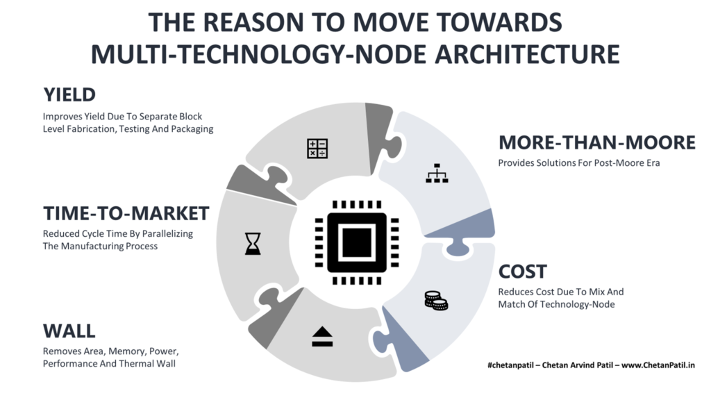
THE REASON TO MOVE TOWARDS MULTI-TECHOLOGY-NODE ARCHITECTURE
There are numerous reasons (and benefits) as to why computer architecture design and manufacturing should move towards multi-technology-node architecture:
Yield: Putting so many blocks together inside an SoC using a single-technology-node architecture design (Example: 7 nm technology-node) brings complexity. It puts constraints not only on the fabrication side but also on testing and packaging. The high-yield for every wafer fabricated with the SoC becomes a difficult task. The electrical testing itself needs to be detailed to ensure that the blocks are working as per the specifications. This complexity quadruples at advanced technology-node like 5 nm and lower. Using multi-technology-node architecture ensures that the different blocks are designed and fabricated with different technology-node. All the higher technology-node (more than 14 nm) are already proven in the market, and this speeds up the fabricating to testing processes. It also massively helps eliminate waste and improves the yield.
Time-To-Market: Proving out the solution at a specific advanced technology-node (using single-technology-node architecture) takes time with numerous SOC components that need to be carefully designed and fabricated in a single die. Any issue with the design or manufacturing eventually increases the time taken to launch the product in the market. Given how stiff the competition is in the semiconductor industry, any delay can cause loss and market position. With multi-technology-node architecture, only specific blocks using new technology-node needs to be more focused on to ensure correctness. The rest of the blocks can take advantage of higher technology-node that have been in use in the market for years and have proven semiconductor process/product.
Wall: The SoC is designed mainly for mobility. Even today, there is no way to provide unlimited direct power to the devices using the SoC in a mobile scenario. Eventually, one has to rely on battery technology to bring mobility. However, fabricating components with thousands of transistors consume power, and improving performance-per-watt (PPW) is becoming a challenge. The SoC design will soon run into area, memory, power, performance, and thermal wall with single-technology-node architecture. Multi-technology-node architecture can provide avenues to bring new ways to manage thermal constraints (using innovative IP from different semiconductor companies) apart from lowering power consumption due to the no area constraints/requirements and also the usage of different types of technology-nodes.
Cost: Shrinking transistor size means adding more manufacturing capacity. The Pure-Play Foundry and IDM have to keep investing in new equipment and process recipes to ensure that the next technology-node is available within two years for any new technology-node launch. All this puts a lot of CapEx pressure on the manufacturing aspect of the SoC using single-technology-node architecture. Apart from manufacturing, the design houses (FAB-LESS/IDM) also have to keep investing in new R&D activities to bring innovation in transistor/device design to enable advanced technology-node process development. With multi-technology-node architecture, existing manufacturing capacity can be used efficiently.
More-Than-Moore: The semiconductor industry is trying to grappling for More-Than-Moore solutions. While there have been many designs for manufacturing processes that are catering to more-than-Moore solutions, multi-technology-node architecture is another approach that takes away the pressure of using the same-technology-node for every block of the SoC. Thus, giving way for another More-Than-Moore solution.
Apart from the above benefits, multi-technology-node architecture brings challenges too. It will require end-to-end semiconductor process validation before being used on a large scale.
THE BOTTLENECKS FOR MULTI-TECHOLOGY-NODE ARCHITECTURE
Multi-Technology-Node Architecture is not in use today. Few years down, it might be a possibility, and to ensure such architecture technique can be fabricated with the blocks of SoC using different technology-node, the following are the two bottlenecks:
Research And Development: Understanding the technical constraints of fabricating blocks of SoC using different technology-node requires research and development efforts. This is to ensure that there is no escape in the architectural process that leads to bigger issues than relying on a single-technology-node architecture way of designing SoC. A close three-way collaboration between Academia, FAB-LESS/IDM, and Pure-Play/IDM is required. Such collaboration requires time to show results. Hence, the research and development activities for multi-technology-node architecture should start today, not tomorrow.
Investment: Initial investment required to prove out the multi-technology-node architecture solutions is high. It requires investing in new software and hardware tools, in order to ensure that the SoC blocks fabricated separately can work in harmony and there are no technical constraints about which technology-node a given blocks used. The semiconductor packaging solution to allow multi-technology-node architecture integration will also be costly due to low scale usage.
As the semiconductor design and manufacturing companies start looking into the possibility of a multi-technology-node architecture, there might be more technical to non-technical bottlenecks apart from the above two.
In any case, multi-technology-node architecture has the potential to provide Post-SoC era computer architectures.
The semiconductor industry has enjoyed the success of doubling (every two years) the number of transistors in a silicon chip, which has allowed semiconductor companies worldwide, to offer novel semiconductor products and solutions. This is exactly what Moore’s law predicted when it was proposed around four decades ago.
Increasing transistor density per given area allows computer systems to cater to multiple (and numerous too) requests at the same time. This is why in 2021 a smartphone is capable of crunching the data that in the 1980s would require a giant server.
However, as the semiconductor world marches towards 3nm mass production (with 2nm already showcased by IBM), there is a growing concern about whether or not Moore’s law will keep pace with the advancement in the technology-node (mainly shrinking transistor size) and what are the alternate solutions.
More-Than-Moore Solutions Have Been In Work For Last Two Decades.
The answer to this problem lies in the different unique solutions that the semiconductor industry has been working around in the last couple of decades. The semiconductor industry knew there is going to be a time when Moore’s law will not be applicable as it is today and a course correction would be needed.
This course correction has led to numerous design to manufacturing changes that have enabled silicon chips to provide more performance and better power consumption without compromising on the area. These solutions have been built on top of different semiconductor product development processes which have come together to drive next-gen workloads without worrying about the future implications of Moore’s law.
Design: To drive innovative solutions that defy Moore’s law by providing similar/better performance and lower power consumption often requires a novel design. These designs can at the circuit level or the system level. The combination of both enables richer design solutions. Like AMD’s chipset-based CPU and GPU design or Appel’s M1 SoC. All these design methodologies drives next-gen solutions that are needed to run future workloads optimally. Such designs often require years of research and development that leads to patents and IP. TVS is another design solution that has allowed novel chip designs.
Node: When it comes to choosing a technology-node for a high-performance device like XPU, the choice is always to go for the best out in the market. This is why companies like TSMC, Samsung, IBM, and Intel are racing to provide the most advanced solution possible. However, the base of the technology-node is a transistor, and to drive a next-gen technology-node that packs more transistor than its predecessor, requires alternate (and better) FET solutions. This is why new scaling CMOS solutions by leveraging new FETs designs is being explored. This started with MBCFETs and soon will move towards forksheet based FETs.
Memory: To drive data-driven workloads efficiently, memory plays a crucial role. As the design changes to accommodate More-Than-Moore solutions, the memory organization and interface also need to change. This has lead companies like Samsung to come up with High Bandwidth Memory (HBM) to power next-gen AI processing solutions. Similarly, Micron has come up with alternate solutions called HBM2E. Advancement in-memory solutions are vital to ensure any Moore-alternate solutions to drive chips are backed up by faster data processing and data transfer.
Package: Silicon chip is nothing but a die from a wafer that gets packaged before being mounted onto the application system. With Moore’s law the internals of the chip was doubling (transistor mainly) to enable more performance, and this has to lead to alternate package technology over the years. This can range from WLCSP to WLFO and beyond. Even the new design methodology of chiplets has to lead to alternate package technology from companies like TSMC, which came up with Chip-on-Wafer-on-Substrate (CoWoS), a 2.5D based package technology to drive next-gen chiplets solutions. To keep up with More-Than-Moore, new package technologies will keep coming out in the market.
Interconnect: As the number of blocks and processing units inside a given chip increases, the need to transfer data faster from one point of the chip to another has also increases. This is why researchers and several companies are focusing on photonics as an alternate. This can ensure the data is not only transferred without adding bottlenecks but also makes sure there is no loss of data. All this while not increasing the power consumption.
Manufacturing: In the end, all design to interconnect process boils down to the fact that whether the solution is manufacturable. New design process and solutions often require close interaction with the equipment manufacturers, FABs and OSATs. This is why, based on years of development, the semiconductor manufacturing industry is moving towards EUV to drive next-gen manufacturing capability. This is going to not only enable 3nm/2nm technology-node but will also drive different package and interconnect solution that have been proposed in the last few years.
Different methodologies discussed above have enabled alternate solutions that leverage Moore’s law but by adapting the new design and manufacturing strategies that ensure there are no bottlenecks.
These solutions range from having a compact chip with all the possible processing blocks to solutions where processing blocks are taken out of the chip and spread across the system. Some solutions also take a different approach of stacking the silicon in such a way that the best of 2D and 3D chip designing comes together to provide a rich user experience.
All these solutions combined are leading the semiconductor industry towards a Moore-Than-Moore world.
The semiconductor industry has implemented several solutions that can be considered as an alternate to Moore’s law and also have been around for many years. These alternate solutions focus on how the design and manufacturing process should be handled to ensure there is always a way to drive more power out of the given silicon chip. All these solutions have been designed without focusing much on the transistor density or technology-node.
It will not be wrong to say that in doing so the semiconductor industry has created itself a pathway to drive into the More-Than-Moore world.
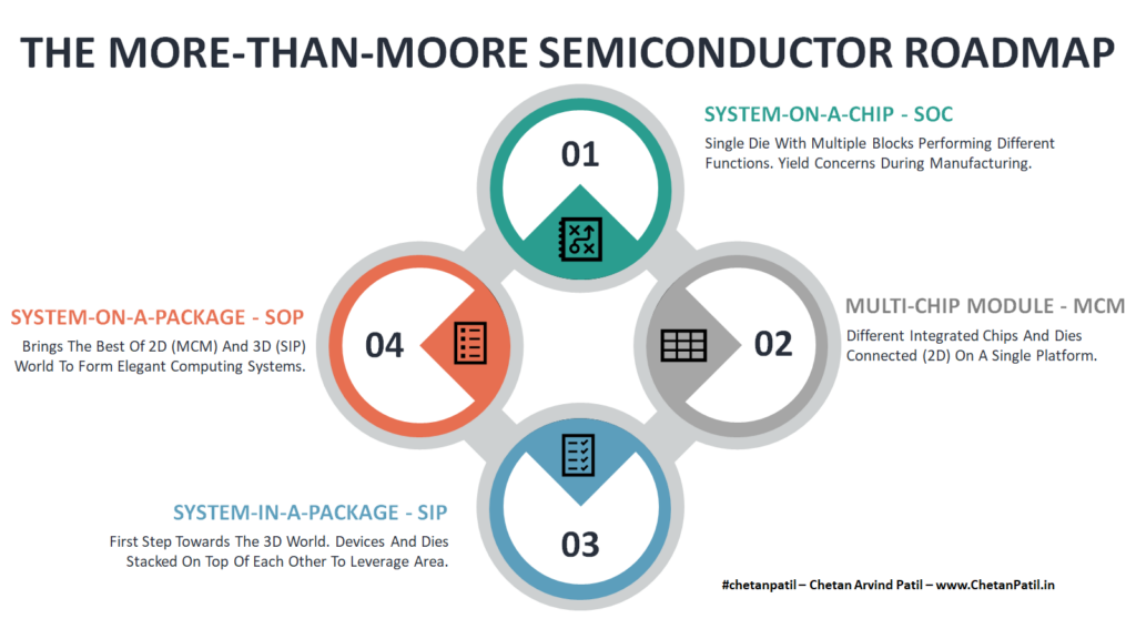
Below are the four major milestones in the last couple of decades that have established the roadmap for the More-Than-Moore world. Few of these have been known to the semiconductor industry for a very long time and little emphasis has been given as to whether this design and manufacturing solution can provide a path towards More-Than Moore or not. In reality, the solution indeed provides a way after Moore’s law ends.
System-On-A-Chip – SOC: SOCs have been around for a couple of decades. The need for multi-core systems coupled with graphics, audio, and video processing lead to SOC. SOC allowed different sub-blocks to reside on a single die area and provided a strong challenge to semiconductor designers and manufacturers. The first major reason was the complexity involved in ensuring the design works as expected and the second reason was the ability to produce high-yielding wafers. SOC has had a mix of both the best and the worst of the semiconductor product development process. Some solutions have to see the end of a life well before the planned date and on another hand, some SOC solutions lasted more than their life span. In the end, SOC provided a way to club complex and required solutions in the smallest area with the help of shrinking transistor size. However, this can only last till the power and thermal profile of the solutions makes technical sense and with challenging process development (shrinking transistor size), SOC may not survive the marking for long but during their time allowed a way to club different features under the same die area.
Multi-Chip Modules – MCM: MCM is a step ahead of SOC. It borrows all the ideas of SOC but brings different types of SOC together on a single platform. The communication between different SOC or ICs is then established using the high-speed interface. This has enabled several XPU (Xeons to Ryzen) based solutions that can diversify the design and manufacturing of the blocks and then leverage interface technology to ensure the data communication is as good or at-par with SOC solutions. Many argue that chiplets design is one form of MCM and in the last couple of years chiplets have taken over the SOC world, and MCM is considered to be the true step towards the More-Than-Moore world.
System-In-A-Package – SIP: SIP takes the best of MCM and SOC to come up with chip solutions that allow 3D-based stacking of different blocks. The interposer or TVS has played a pivotal role in enabling SIP. The goal of SIP is to take the 2D area and covert it into 3D by stacking the different blocks of SOC/MCM on top of each other. This way the area consumption decreases which 2D solutions like SOC and MCM cannot achieve without using advanced technology-node. SIP does have a drawback as they suffer from thermal and packaging challenges. With advanced technology-node nearing 1nm, SIP might be the best More-Than-Moore solution to provide an alternative to chip designing compared to MCM and SOC.
System-On-Package – SOP: All the above three More-Than-Moore alternate solutions are designed with the focus that the end system is going to be printed circuit board on top of which the SOC/MCM/SIP system will reside. However, this does not help the smaller devices like smartphones where the goal is to ensure that there is more room for battery by shrinking the board area. To shrink the board footprint, SOP is the best way to design a computing system. SOP takes different chips (either a SOC, MCM, or SIP) and then brings all these individual chips inside a single package. The complexity to achieve an elegant SOP system is way too high. It requires not only synchronization of different types of system/devices (SOC/MCM/SIP) but also a standard interface that can allow packaging of all devices while ensuring that there is no bottleneck or leakage. SOP if done correctly might very well end the need for board and allow a more compact silicon solution while defying Moore’s law.
The above four semiconductor design and manufacturing alternatives certainly provide a way to design chips (mainly XPU) such that there is no need to worry about packing more transistors in the smallest area.
From SoC to SOP, the solutions simply take the silicon area out of the context by bringing different sub-systems together but in a unique way, and it pushes the FABs and OSATs to come up with manufacturing technologies (which many FABs and OSATs already have) that can ensure the sub-systems work seamlessly even though there are disaggregated.
As the semiconductor industry inches towards 1nm technology-node, SOC/MCM/SIP/SOP based chip solutions are certainly going to provide a roadmap for More-Than-Moore solutions.
Cells are the building blocks of life. Similarly, transistors are the building blocks of the semiconductor industry. In the computing world, transistors lay the foundation for any type of processing solution.
Transistor performs the basic function of toggling between HIGH (ONE/TRUE) and LOW (ZERO/FALSE) state. Such basic function when performed by zillions of transistors together, drives several technological solutions from car safety to wireless data/voice transmission.
The need to make compact computer-powered solutions has pushed the development around the transistors over the last four decades. These development have been both on the design and the manufacturing side.
Transistors used in semiconductors are often called FET – Field-Effect Transistors. The function performed by FETs is the same as traditional transistor. The only aspect that has changed over the years is the form factor which changed in order to follow the Moore’s law.
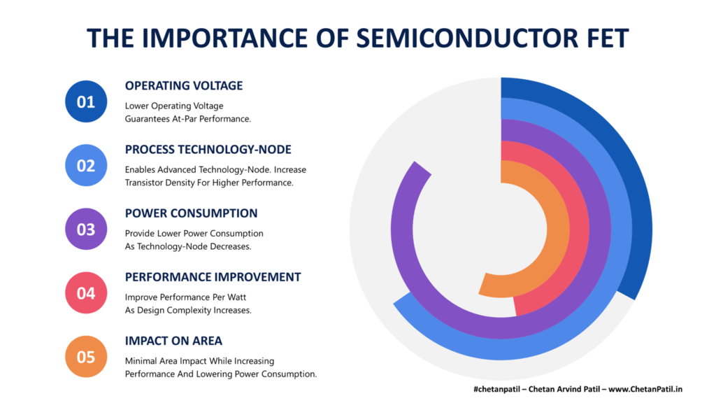
The main goal of FET is to improve Power-Performance-Per-Area (PPA). To do so, following technical aspect has to be fulfilled before the FET design can be used to manufacture next-gen hardware:
Operating Voltage: A perfect FET will be the one that can perform as per the specifications. As the technology-node shrinks, the operating voltage also goes lower due to the advancement in the FET design. The major reason is to accommodate the dynamic and static power consumption along with the leakage. Lowering voltage has negative impact to, but that is compensated with the unique designs of next-gen FET.
Process Technology-Node: Technology-Node shrinks faster than the development of new devices. Till then the devices go through a different non-planar to planar transformations to accommodate for the shrinking size. However, after a given point it becomes design and manufacturing-wise difficult to transform (like FinFET can only be stretched to a certain extent with the help of its fins) the same device type. After that, the material and drastic design changes are expected.
Power Consumption: FETs are present in a large number in any advanced technology-node systems like microprocessors. If FETs are not providing the lower dynamic power consumption (along with negligible leakage), then the purpose to use new designs is not fulfilled. Hence, device designers face an uphill challenge to ensure the increased density of the FET in a specific silicon area only leads to lower power consumption, not higher.
Performance Improvement: Apart from lower power consumption, performance improvement is another criterion that leads to new FET designs. Balancing power consumption along with performance is difficult. However, without these criteria, there is no way to ensure the next technology-node will have a better impact and use case than the previous one.
Impact On Area:Eventually, the goal of shrinking technology-node is to ensure the area of the silicon chip does not increase for the same or more computing tasks. This means the design of new FETs will have to be more 3D than 2D/2.5D. Otherwise, in the long run, it becomes a bottleneck for the designers to make use of the FET without impacting the silicon area.
The FET is the building block of modern semiconductor solutions and there are already several types of FET that are available and used based on the technology-node.
Both academia and the industry have contributed equally in bringing new FET design to the market, which today is powering almost all of the electronic products around the globe.
Given the race to be the first one to launch the next technology-node, the semiconductor companies (mainly semiconductor manufacturers) are also racing to come up with a new FET design that can cater to their needs while having minimal to zero impact on Power-Performance-Per-Area (PPA). During this course, the semiconductor industry has already seen many transformations in FET designs. From 2D to 3D.
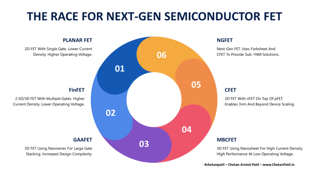
Below are few active and future FET designs that the semiconductor manufacturer is pursuing:
Planar FET: These are the traditional FET that follow the 2D design. The source, the drain is on top of the substrate and is not wrapped around the gate. The power consumption and area impact is high. Planar FET mostly use nanowires.
FinFET: FinFET is an advanced version of planar FET. The source and drain are extended as fins and the gate wraps around them to provide a faster current flow. One drawback of FinFET is that the design might lead to manufacturing residuals around the fins. This can impact the quality of silicon chip being manufactured. However, FABs have found ways to ensure there are enough inspection steps to avoid such defects. FinFET is what today the majority of the manufacturing companies use to manufacture silicon requiring advanced technology-node.
GAAFET: FinFET has its advantage, however, to provide lower operating voltage and higher performance, the industry has also come up with GAAFET. GAAFET is geared to be used towards 3nm mass production along with FinFET. The difference between GAAFET and FinFET is the slicing of fins by making of nanosheets to drive much faster current flow that FinFET. This also allows greater switching control. This structure helps in shirking the size without impact the performance.
MBCFET: MBCFET has been developed by Samsung as part of their 2nm and beyond technology-node roadmap. Both FinFET and GAAFET use fins that are stacked vertically, thus not allowing the use of the area above the source and drain. To overcome this, MBCFET is developed that uses the same fins based nanosheets but are stacked horizontally to provide more area for current flow. MBCFET can also be designed using existing process tools and has the same area footprint as FinFET and GAAFET.
CFET: While the industry moved towards fin-based structure and started using nanosheets to provide more area within the same size, researchers have also been focusing on CFET which they are touting to be the next-big thing in FET design. The CFET is an advanced version of fin-based FET (even more advanced than MBCFET) and it uses the folding approach to keep nFET on top of the pFET. This can be done either via fins or sheets. It is like a high-rise structure with FETs stacked on top of each other. CFET still uses a nanosheet approach.
NGFET: These do not exist today. NGFET – Next-Gen FET – will be what the semiconductor industry will use when going beyond 1nm. It will borrow all the learnings from the prior generation, however, instead of nanosheet, NGFET will use forksheets. The forksheets will take a nanosheet approach by combining the vertical and horizontal fins to provide more density and performance.
While there are several FET solutions to choose from, the industry and the academia do understand the difficulties the semiconductor design and manufacturing bring when advanced technology-node process is used. Thus, leading to several new (and known) hurdles and challenges.
Given the small area for improvement, new FETs are incredibly complex to design. While both the academia and the industry is focused on improving the FET design that lowers the operating voltage while balancing other technical specifications, there are certainly numerous hurdles to overcome.
Voltage: The smaller/advanced the technology-node, the lower the operating voltage. The primary reason is the ability to generate heat or damaging the devices (= FETs) when operated at a higher voltage. With every new generation/type of FET, the operating voltage is low. This also impacts the sub-sequent systems the advanced technology-node systems (using lower operating voltage FETs) are connected to. This means a new system is required to drive the data further at higher voltages. As FETs evolve beyond 3nm technology-node, such design constraint is something the device designers will have to consider so that the operating voltage is not too low for the silicon system down the line.
Leakage: Lowering technology-node means new device structures and it also means more transistors per given area. Operating all these devices at higher voltage can subsequently lead to leakage either through continuous operation or via thermal. Lowering the leakage is another challenge for FET device designers.
Thermal: Thermal is a tricky one to solve. The junction temperature is already high enough that it demands designers to embed temperature sensors to capture thermal effects. This certainly adds complexity to the design and also impacts the operating scenarios, which hinders from exploiting the full potential of the systems due to continuous throttling.
Performance: Lowering operating voltage as the FET evolves means also balancing the performance and area ratio. FET in the future will have tackle this three-way balancing act (voltage, performance, area) as the industry marches towards the 2nm and lower technology-node.
There are certainly several hurdles (apart from those listed above) for FET design and manufacturing. The semiconductor design and manufacturing industry will overcome these and many. Academia is also coming up with interesting FET solutions that can pave way for more elegant lower technology-node solutions without compromising on the voltage to performance to silicon area.
In the end, the FET design will keep changing and evolving in order to keep pushing the semiconductor industry forward towards More-Than-Moore world.