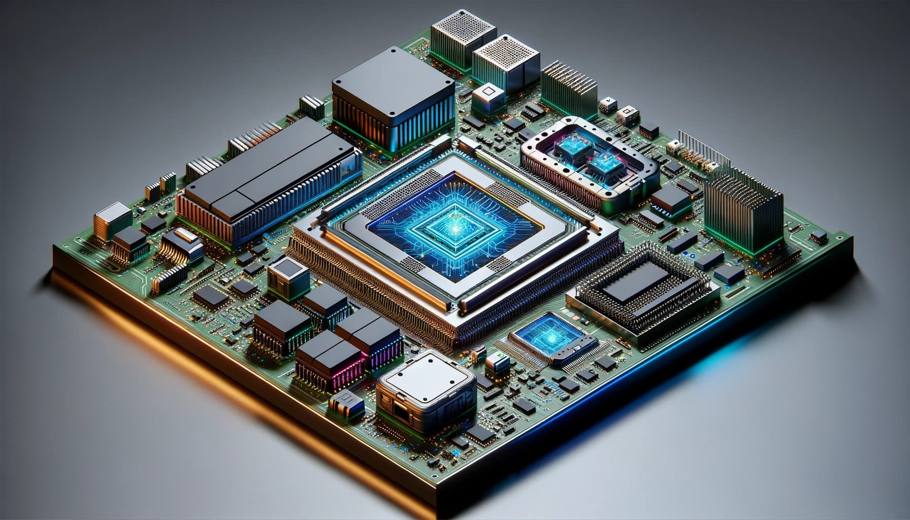
As artificial intelligence (AI) incorporates itself into various industries, the demand for more sophisticated computing power is rising. At the core of this technological evolution is the development of semiconductor AI centers, a concept that promises to redefine the future of computing.
This transition is marked by several key projects, such as Microsoft and OpenAI’s ambitious plan to build a supercomputer named “Stargate,” rumored to be one of the most advanced and costly (more than $100 Billion) endeavors in computing history.
Such semiconductor AI centers are about more than just scaling up. They represent a shift towards custom chip designs, aiming to break free from traditional dependencies and push the boundaries of what’s possible with AI.
The implications for the semiconductor industry are profound, signaling a move towards more specialized, efficient, and powerful computing solutions.
How AI-Center Differ From Traditional Data Centers
These specialized AI center facilities provide enhanced computational power and efficiency and will facilitate groundbreaking AI research and application innovations.
Below is a comparison of critical differences between AI-centered and traditional data centers.
Feature
AI-Centered Data Center
Traditional Data Center
Computational Power
Customized for AI workloads, equipped with specialized processors (GPUs, TPUs) for high-performance computing.
General-purpose computing, relying on standard CPUs with limited AI optimization.
Energy Efficiency
Designed with energy-efficient technologies and cooling systems to manage the high power consumption of AI processing.
Often less efficient in energy use due to older designs and cooling technologies.
Scalability
Highly scalable to meet the exponential growth of AI demands, supporting large-scale AI model training and inference.
Scalability is limited by the design and technology of traditional computing and storage systems.
Networking
Advanced networking capabilities, including high-bandwidth connections and low-latency networks for AI data processing.
Standard networking setups, which may not support the high-speed data transfers needed for intensive AI tasks.
Innovation Focus
Aimed at pioneering AI research and development, pushing forward new AI applications and technologies.
Focused on maintaining operational efficiency and reliability for a broad range of IT services.
However, with the benefits comes the challenges, and addressing these challenges is crucial for leveraging AI’s full potential and ensuring the sustainable growth of AI-centered infrastructures.
Energy Consumption: AI centers consume vast amounts of electricity for processing and cooling, posing sustainability and cost challenges.
Heat Management: The high-performance computing units generate significant heat, requiring advanced cooling solutions.
Data Security: Protecting the massive data pools processed and stored in AI centers from breaches and attacks.
Skilled Workforce: There is a high demand for professionals with expertise in AI, machine learning, and data center management.
Technology Advancement: Keeping up with the rapid pace of AI and computing (mainly silicon) technology advancements to remain competitive.
Near-Term Roadmap Of AI-Centers
The near-term roadmap for AI centers will address scalability, energy efficiency, and computational challenges to meet the growing demands of AI applications.
Priorities include integrating advanced cooling technologies, developing sustainable energy sources, and adopting next-generation computing architectures.
These efforts will enhance AI model training and deployment capabilities while minimizing environmental impact and operational costs.
Nevertheless, the development of the AI center promises to enhance AI computational capabilities and open new avenues for innovation across industries, heralding a new era of technological advancement.
General Purpose GPUs (GPGPUs) represent a significant evolution in computing, transforming GPUs from specialized hardware focused solely on graphics processing to versatile computing units capable of handling a broad range of tasks. This shift has enabled GPUs to play a crucial role in areas beyond gaming and graphics, including scientific research, data analysis, and artificial intelligence (AI). By leveraging their parallel processing capabilities, GPGPUs can execute complex mathematical and data-intensive operations at speeds vastly superior to traditional CPUs, making them indispensable for tasks requiring high computational throughput.
Traditionally, GPUs are designed and manufactured as monolithic dies, where a single silicon die houses all the GPU’s functionalities. This approach has advantages, such as straightforward design, manufacturing processes, and high-speed internal communication. However, it also faces limitations in scalability, manufacturing yield, and adaptability to rapidly evolving computational demands, especially those driven by artificial intelligence (AI).
AI Specific GPU
As the demand for more versatile and powerful computing resources grows, particularly in AI-driven applications, the semiconductor industry is witnessing the next leap in innovation: the rise of Ghiplet architecture.
Ghiplet technology takes the concept of versatility and scalability to a new level. By adopting a modular approach, where a GPU gets built from multiple interconnected ghiplets, Ghiplet architecture offers unprecedented flexibility in GPU design. This modularity allows for optimizing specific functions, such as AI computations or memory handling, within individual Ghiplets, which can then be customized to meet the unique requirements of various applications.
Furthermore, the Ghiplet approach addresses some of the critical challenges faced by monolithic designs, such as manufacturing yields and the rapid pace of technological advancement, heralding a new era of GPU technology that is adaptable, efficient, and ready to meet future computing demands.
Ghiplet = G(PU) + Chiplet
Flexible And Scalable
Ghiplet architecture allows for unprecedented flexibility and scalability in GPU design. Depending on an application’s specific needs, different combinations of ghiplets can be assembled to optimize performance, power efficiency, or cost. It starkly contrasts monolithic designs, where changes in functionality or performance often require a complete redesign of the silicon die.
One of the significant challenges with monolithic dies is the lower yield rates associated with manufacturing large and complex silicon pieces. Defects in any part of the die can render the entire chip unusable, increasing waste and cost. Ghiplet architecture mitigates this issue by using smaller, more manageable ghiplets. Since ghiplets are produced separately, a defect in one ghiplet doesn’t necessitate discarding the entire GPU, significantly improving yield rates and reducing production costs.
A crucial aspect of making Ghiplet architecture viable is the development of advanced interconnect technologies. These technologies ensure fast, efficient communication between ghiplets, which is essential for maintaining high performance. Innovations such as silicon photonics and advanced packaging solutions, like 2.5D and 3D stacking, are pivotal.
They enable Ghiplet GPUs to achieve and sometimes surpass, their monolithic counterparts’ communication speeds and bandwidths, overcoming one of the leading technical challenges of modular design.
AI-GPU For AI-Workload
AI’s computational demands are a major driving force behind the shift towards Ghiplet architecture. AI applications require massive data processing, often necessitating specialized hardware accelerators. Ghiplet GPUs can integrate AI-specific ghiplets, offering tailored solutions that are more powerful and energy-efficient than monolithic designs can typically provide.
This adaptability is crucial for staying at the forefront of AI technology development.
Modular Future
The Ghiplet concept represents not just a technological innovation but a paradigm shift in how we think about GPU architecture, especially in the context of AI. Understanding the principles and potential of Ghiplet technology is essential for students and future engineers. It offers insights into the future of computing, where flexibility, efficiency, and specialization become critical drivers of semiconductor design.
As the industry continues to advance, the modular, ghiplet-based approach heralded by Ghiplet technology is set to play a pivotal role in shaping the next generation of computing devices, making it a critical area of study and exploration for anyone interested in cutting-edge semiconductor technology.
Semiconductor testing, also known as integrated circuit (IC) testing or chip testing, is a critical process in the semiconductor manufacturing cycle. It verifies that ICs function before being deployed in various applications, ranging from consumer electronics to critical automotive systems. This testing phase ensures that only devices meeting the required performance, functionality, and reliability specifications reach the market.
In a nutshell, semiconductor testing involves applying electrical signals to a chip and measuring the output to assess its performance against predefined criteria. The process is carried out using specialized equipment known as automated test equipment, capable of conducting various electrical tests. Testing can occur at several stages of the semiconductor manufacturing process, including:
Wafer Testing (Wafer Sort): Test individual chips while still part of the silicon wafer before they are cut out and packaged.
Package Testing (Final Test): Testing the chips after they have been packaged to check for defects at the final stage.
Burn-In Testing: Exposing chips to stress conditions (e.g., high temperatures, voltage) to identify early failures.
The results from semiconductor testing provide valuable feedback to both designers and manufacturers, highlighting potential areas for improvement in chip design and fabrication processes. This feedback loop is crucial for advancing semiconductor technology and increasing yields.
Test Program And Time Taken
The development and execution of semiconductor test programs involve several challenges that can significantly extend the time and resources required:
Complexity: As semiconductor technology advances, chips become more complex, integrating billions of transistors into an ever-smaller area. This complexity makes the test program development more intricate and time-consuming.
Diverse Test Requirements: Each semiconductor product has unique test requirements based on its application, ranging from consumer electronics to automotive systems. Tailoring test programs to these specific needs adds to the development time.
High Coverage Requirement: High fault coverage is essential for reliability but requires comprehensive test scenarios and patterns, increasing test time.
Evolving Standards And Technologies: With continuous advancements in semiconductor technologies and standards, test programs must also evolve, necessitating frequent updates and revisions, which are time-intensive.
Equipment Utilization: Efficient use of expensive test equipment is crucial. Balancing thorough testing with efficient use of test resources is a constant challenge, as more extensive testing can lead to higher costs and longer test times.
Given the critical role of semiconductor devices in modern technology, the importance of thorough testing cannot be overstated. It is the final safeguard against defects and failures that could have widespread implications for manufacturers, consumers, and entire industries relying on these components.
The advancement of testing methodologies, including the integration of AI and machine learning, continues to be a key focus area for improving the efficiency and effectiveness of this crucial process
Integrating Artificial Intelligence (AI) into the generation of semiconductor test programs represents a transformative approach to enhancing efficiency, coverage, and speed in the semiconductor manufacturing process.
The technical integration of AI can be segmented into several key areas, utilizing a variety of AI methodologies including machine learning (ML), deep learning (DL), reinforcement learning (RL), and neural networks.
A few potential use cases of AI in semiconductor test program generation:
Automated Test Pattern Generation: AI algorithms can automate the creation of test patterns, significantly reducing the time and expertise required to develop test programs manually. This automation can adapt to the complexity of the semiconductor device, ensuring comprehensive coverage more efficiently.
Predictive Fault Detection: AI can analyze historical test data to predict potential failure points in new chip designs. This predictive capability allows for targeted testing of high-risk areas, reducing the overall testing time without compromising fault coverage.
Optimization of Test Sequences: AI can optimize the sequence of test patterns to minimize the test time while maximizing fault coverage. This optimization includes identifying and eliminating redundant tests and prioritizing tests based on their likelihood of uncovering defects.
Adaptive Testing: AI-enabled test programs can dynamically adjust testing parameters in real-time based on interim results. This adaptability ensures more efficient use of test resources, focusing efforts where they are most needed.
Learning from Data: AI models improve over time, learning from every test executed. This continuous improvement cycle can lead to increasingly efficient test programs, reducing time and cost with each iteration.
By leveraging AI, the semiconductor industry can address the significant challenges associated with test program generation.
Future Course
The integration of AI in semiconductor test program generation is a transformative approach, leveraging advanced AI techniques to address the complexity and scale of modern semiconductor testing challenges.
By utilizing AI, the semiconductor industry can address the significant challenges associated with test program generation. AI not only promises to reduce the time and cost associated with testing but also improves the reliability and performance of semiconductor devices, ultimately benefiting manufacturers and consumers alike.
In 2020, I wrote an article titled “The Status Of Semiconductor Manufacturing In India,” focusing on the status of India’s semiconductor ecosystem at the time. Since then, India has seen substantial developments and strategic shifts toward establishing a self-reliant semiconductor ecosystem.
India’s journey towards becoming a key player in the global semiconductor manufacturing space has accelerated by significant government support, strategic international partnerships, and a focus on building a comprehensive ecosystem that includes fabrication, assembly, and testing, as well as research and development, including the support ecosystem (equipment, tools, and so on).
Conversely, the Indian semiconductor market is forecasted to reach over $60B+ by 2026, driven by demand in smartphones and wearables, automotive components, and computing and data storage sectors, with an anticipated market size of more than $100B+ and an additional half a million (direct and indirect) jobs to be created by 2030. Thus, India’s semiconductor ecosystem is a crucial contributor to the global industry’s growth to $1 trillion by 2030.
Semiconductor Fabrication In India
The fabrication segment is witnessing a series of transformative investments, notably with the entry of major international and domestic players. Powership Semiconductor Manufacturing Corporation (PSMC) and Tata Electronics have partnered to establish India’s first semiconductor wafer fabrication plant in Gujarat. The plant’s focus on advanced 28nm technology nodes underscores India’s readiness to cater to domestic and global markets.
The Indian government’s commitment to nurturing the semiconductor fabrication ecosystem is evident through increased capital outlays and supportive policies. The 2024-25 budget saw a remarkable 100% increase in capital outlay for semiconductor and display manufacturing development, reaching close to a billion dollars. This substantial financial boost, coupled with the Semicon India Program and incentives for setting up fabrication units, underlines the strategic importance placed on semiconductor manufacturing within India’s broader economic and technological policy framework.
Micron Technology’s establishment of an ATMP facility in Gujarat is a pivotal development in the assembly and testing landscape. This initiative marks a significant milestone, being one of the first in India. The facility, representing more than a $3B+ investment, signifies the potential for India to become a hub for semiconductor assembly and testing, catering to local and international markets.
Additionally, the Tata Group is establishing an ATMP facility in Assam, and a joint venture between CG Power, Renesas Electronics, and Stars Microelectronics is setting up an OSAT facility in Gujarat. These investments, valued at $15B+, are expected to contribute significantly to India’s semiconductor market growth.
Semiconductor Design In India
India is home to every top semiconductor company that designs silicon chips, and the sector is witnessing significant growth, underscored by its robust talent pool and strategic initiatives aimed at enhancing its global footprint in semiconductor design and innovation. These engineers are integral to global semiconductor companies and domestic design service firms, engaging in developing cutting-edge chips across various stages, from specifications and architecture to design and physical verification.
The country’s design engineers have the needed semiconductor skills and competencies, with contributions spanning across the design process and impacting complex Integrated Circuits (ICs), Application-Specific Integrated Circuits (ASICs), and Systems on Chips (SoCs) globally. This recognition is domestic and international, with corporate leaders from significant semiconductor firms acknowledging the caliber of Indian engineers. This talent pool’s prowess also attracts substantial investment from global companies looking to expand their design and engineering capabilities in India.
The Indian government is actively supporting this segment through various initiatives. One notable scheme is the Design-linked incentive (DLI) scheme, which offers a matching 50 percent government investment to support enterprise launches, along with “deployment-linked” incentives based on criteria like the use of Indian-made content. This initiative targets the design of ICs, chipsets, SoCs, systems, IP cores, and semiconductor-linked methods, explicitly catering to indigenous companies engaged in semiconductor design and IP development.
Future Of Semiconductor In India
India still has a long way to go before competing with leading global semiconductor powerhouses (mainly the EU, East Asia, and the US). One critical area in which India needs to focus is enhancing its research and development infrastructure and capabilities.
To truly compete on the global stage, India must ensure a sustained, long-term commitment to its semiconductor industry, spanning government policies, industry collaborations, and academic contributions. It involves financial investment and a strategic focus on upskilling the workforce, fostering innovation, and creating an attractive environment for domestic and international semiconductor firms.
Exciting times are ahead for India’s semiconductor ecosystem.
The dominance of semiconductor giants like NVIDIA, with a market capitalization exceeding $3 trillion, and TSMC, valued at nearly $700 billion, among the top 10 largest companies globally, underscores the seismic shift towards a semiconductor-driven economy.
These (and many other) firms, pivotal in the semiconductor industry, highlight the sector’s critical role in underpinning most of today’s technological landscape. With semiconductors at the heart of an array of technologies – from artificial intelligence and data centers to consumer electronics and automotive systems – this industry’s influence mirrors the transformative power of oil in the previous century.
The stark representation of semiconductor firms among the elite global corporations (by market cap) illustrates their economic significance. It signals the dawn of an era where technological innovation, powered by semiconductors, is the new currency of global dominance.
This transition spotlights the undeniable fact that semiconductors have become the ‘new oil,’ essential for fueling the future of global technology and economy.
The rise of semiconductors can be traced back to the mid-20th century, marking a revolution in technology and engineering. Initially, the industry was focused on simple diodes and transistors. Still, by the 1960s, the invention of the integrated circuit paved the way for the microprocessors that would eventually power personal computers, mobile phones, and many other devices.
By the 1980s and 1990s, advancements in semiconductor technology allowed for exponential increases in computational power, adhering to Moore’s Law, which predicted a doubling of transistors on a chip approximately every two years. This growth has continued into the 21st century, with the semiconductor market size reaching over $425 billion in revenue by the early 2020s, underlining the critical role of semiconductors in global technological progress.
The semiconductor industry, projected to reach a $1 trillion market by 2030, plays a pivotal role in the global economy, contributing to approximately $3 trillion in GDP from 1995 to 2015 and an additional $11 trillion in indirect impact. This industry’s significance is further highlighted by its accelerating growth, doubling its importance relative to global GDP over the last three decades. Moreover, the U.S. semiconductor sector’s investment in R&D, totaling $58.8 billion in 2022, underscores its commitment to innovation, with R&D expenditure surpassing 15 percent of sales for over two decades.
The semiconductors’ trajectory has been remarkable, evolving from essential components to the backbone of advanced computing systems and consumer electronics. This surge reflects the expanding demand for electronic devices, cloud computing, and data centers, driven by digital transformation across industries. The semiconductor’s role in technology’s future is underscored by substantial investments in research and development, aiming to push the boundaries of what these tiny yet powerful chips can achieve.
In today’s rapidly evolving world, semiconductors are the cornerstone of modern technology, quietly powering the digital age from behind the scenes.
They are not just components; they are the architects of our digital reality, enabling the seamless operation of networks, processing vast amounts of data, and developing cutting-edge technology. As the world ventures into an era defined by artificial intelligence (AI), the significance of semiconductors becomes even more apparent, cementing their status as indispensable drivers of global progress and innovation.
Without these microscopic marvels, the technological advancements that define our current lifestyle and promise an even more interconnected and intelligent future would not be possible.
The semiconductor industry is not just a part of the future economy. It is poised to be a cornerstone, driving innovation and growth across multiple sectors. Here are several statistics-based arguments that illustrate this trend:
ASPECT
STATS
Market Growth
The global semiconductor market was valued at around USD 425 billion in 2020 and is expected to grow at a CAGR of approximately 6.8% from 2021 to 2028, driven by demand in automotive, consumer electronics, and industrial applications.
Innovation And RnD Investment
The industry allocates 15-20% of sales revenue to RnD, surpassing many other sectors, underscoring a commitment to innovation and future growth.
Impact On Other Industries
Semiconductors underpin modern technology and are vital for AI, 5G, and IoT advancements. For example, 5G deployment relies on advanced semiconductor technology.
Economic Multiplier Effect
Each job in the semiconductor sector generates approximately 4.89 additional jobs in other economic sectors, demonstrating the high value-add of semiconductor products and their extensive supply chain.
Global Supply Chain And Trade
The semiconductor industry is a worldwide trade powerhouse with international sales and supply chains, supporting economic growth and fostering international technological exchange.
Sustainability And Energy Efficiency
Semiconductors enable energy-efficient solutions like electric vehicles and smart grids, contributing to reduced energy consumption and alignment with global sustainability goals.
Semiconductor Everywhere
Governments worldwide are rapidly awakening to the critical importance of semiconductors, recognizing them as the backbone of modern technology and a crucial element of national security and economic prosperity. In an era where technology underpins every aspect of daily life, from communication and entertainment to transportation and defense, the role of semiconductors has become increasingly central.
This realization is prompting nations to reassess their strategic priorities, leading to a surge in investments, policy reforms, and international collaborations to secure semiconductor supply chains and boost domestic production capabilities.
By acknowledging the semiconductor industry’s pivotal role in advancing technological innovation, ensuring military readiness, and driving economic growth, governments are now placing semiconductor strategy at the forefront of national agendas, marking a significant shift towards securing technological sovereignty in a rapidly evolving global landscape.
Here are eight ways in which countries are investing in semiconductors:
ASPECT
DETAILS
Funding And Tax Incentives
Countries provide grants for new factories, R&D subsidies, and tax breaks to attract semiconductor companies, supporting manufacturing and research.
Building Semiconductor Ecosystems
Efforts are made to create comprehensive semiconductor ecosystems, including manufacturing, design, RnD, and support for startups, universities, and research institutions.
Strategic Partnerships And Alliances
Forming strategic partnerships and alliances with nations, companies, and research institutions to secure supplies and advance technological capabilities.
Education And Workforce Development
Investing in education and training programs to develop a skilled workforce, including specialized university programs and technical training.
Research And Development Investments
Making significant investments in RnD to advance semiconductor technology, focusing on next-generation materials, chip design, and manufacturing processes.
Supply Chain Resilience
Taking measures to ensure the resilience of semiconductor supply chains, including diversifying sources and investing in domestic manufacturing capabilities.
Attracting Foreign Investment
Working to attract foreign semiconductor companies through incentives, regulatory support, and infrastructure development, integrating more deeply into the global supply chain.
National Security Measures
Implementing measures to protect semiconductor industries for national security, including restrictions on foreign investments and securing intellectual property rights.
Take Away
In the contemporary landscape, where semiconductors play a pivotal role in driving technological advancement and economic growth, understanding the multifaceted impact of this industry is essential for a diverse array of stakeholders.
For students, the ascendance of semiconductors underscores the critical importance of engaging with STEM disciplines, highlighting the opportunity to be at the forefront of technological advancements. Professionals, particularly those within the realms of technology and manufacturing, are reminded of the necessity to perpetually enhance their skill sets in alignment with the industry’s dynamic nature. For the industry at large, the pivotal role of semiconductors emphasizes the imperative of fostering innovation, facilitating international collaborations, and prioritizing research and development to maintain competitiveness on the global stage. Governments are called upon to recognize the strategic importance of the semiconductor sector, advocating for policies that bolster industry support, ensure the resilience of supply chains, and promote technological progress. Collectively, these insights articulate the transformative influence of semiconductors and their indispensable position in steering the direction of our digital future.
The semiconductor industry’s influence extends far beyond the confines of technology firms, touching upon education, professional development, industrial strategy, and governmental policy. As the world delves into the implications of semiconductors’ ubiquitous presence in our digital era, examining the takeaways for critical groups such as students, professionals, the broader industry, and government entities is imperative.
This perspective highlights the critical importance of semiconductors and sheds light on the collective and individual roles in embracing and advancing this dynamic field of semiconductors.
Artificial Intelligence (AI) has emerged as a cornerstone in the rapidly evolving computing technology landscape, driving innovation across various sectors. At the core of AI’s transformative power are specialized silicon chips, AI Systems on Chips (SoCs), designed to process AI algorithms efficiently. These chips are pivotal in enhancing the performance and capabilities of AI applications, from autonomous vehicles and smart devices to data centers and beyond.
As AI continues to integrate into our daily lives, the companies behind these advanced SoCs play a critical role in shaping the future of technology. This list introduces the AI SoC companies taking different approaches to designing SoCs for AI applications, spotlighting their contributions to the AI revolution and their impact on the tech industry.
Below is a work in progress, and if you find AI SoC companies that still need to be listed here, please do reach out to me.
Company
Description
Ambarella
AI Vision Processors For Edge Applications
Alphawave
Provides DSP solutions for high-speed, low power consumption, enables building AISoC with AppolloCORE IP, winner of TSMC’s Awards for Excellence.
Anari AI
Creating cutting-edge technology to make things work in accordance with the intelligent and scalable future
Axelera AI
Revolutionising the field of artificial intelligence by developing a cutting-edge hardware and software platform for accelerating computer vision on edge devices
Axiado
To secure the end-to-end digital infrastructure by embedding a new breed of hardware-anchored AI-driven platform security in servers, 5G and network infrastructure
Blaize
Blaize has created a transformative new compute solution that unites silicon and software to optimize AI from the edge to the core
BrainChip
Specializes in developing advanced artificial intelligence and machine learning hardware
Celestial AI
Celestial AI is the creator of the Photonic Fabri, an optical interconnect technology platform for compute and memory
Cambricon Technologies
Founded in 2016, Cambrian focuses on the research and development and technological innovation of artificial intelligence chip products
Cerebras Systems
Uses Wafer-Scale Engine technology for deep learning, claimed to be 1000 times faster than a GPU, with innovative interconnects, memory, and package technology
EdgeQ
Fuses Edge and 5G into a single AI-powered chip, aiming to off-load tasks from data centers to Edge Computing
Enfabrica
Hardware, software, and system technologies that solve the critical bottlenecks in the next generation AI SoCs
Esperanto Technologies
Esperanto delivers high-performance, energy-efficient computing solutions that are the compelling choice for the most demanding AI applications
EnCharge AI
Leader in advanced hardware and software systems for AI computing
Flex Logic
Developer of embed field-programmable gate IP focused on AI SoC
GrAI Matter Labs
Created the fastest edge AI processor for machine vision in robotics, AR/VR, drones and more
Graphcore
Has built a new type of processor for machine intelligence to accelerate machine learning and AI applications for a world of intelligent machines
Groq
Leverages Tensor Streaming Processor (TPU) for high-speed memory and fast operations, packed in a tiny package
Hailo
Focuses on Edge AI, claims its Hailo processor can deliver better TOPS with high area and power efficiency
Horizon Robotics
Designed AI-enabled Brain Processing Units (BPU) for the automotive (Journey BPU) and IoT (Sunrise BPU) markets
Habana
Creates world-class AI Processors, developed from the ground-up and optimized for training deep neural networks and for inference deployment in production environments
Kneron
Develops an application-specific integrated circuit and software that offers artificial intelligence-based tools
Kinara
Kinara processors drive AI applications demanding low latency, high performance, and low power
LeapMind
Focuses on edge AI and machine learning
Lightelligence
Providing customers with powerful and effective computing power through a new paradigm of optoelectronic computing
Lightmatter
Chip architecture, powering faster, energy-efficient computing with photonic processors for sustainable AI advancement
Luminous Computing
Leverages photonics for faster AI workload training, still in stealth mode
Mythic AI
Utilizes Intelligence Processing Units (IPUs) for efficient, performance-oriented, cost-efficient AISoC, offers Mythic Analog Matrix Processor
Neureality
Developing AI inferencing accelerator chips
Prophesee
Uses a patented sensor design and AI algorithms that mimic the eye and brain to reveal what was invisible until now using standard frame-based technology
Rebellions
Develops AI accelerators by bridging the gap between underlying silicon architectures and deep learning algorithms
Rain Neuromorphics
Building the most energy efficient hardware for AI
SambaNova Systems
AI hardware and integrated systems to run AI applications from the data center to the cloud
SiMa.ai
Aims for greener, low-power AISoC for Edge AI, details forthcoming, plans new silicon launch
Synthara AG
Enables seamless integration of in-memory computing capabilities to existing chip designs, making them 130 times faster and 150 times for energy efficient
Syntiant
Leader in edge-AI deployments, bringing deep-learning to any device with industry-leading Neural Decision Processors and hardware-agnostic machine learning models
Tenstorrent
Next-generation computing company that utilizes RISC-V that builds computers for AI
Wave Computing
Accelerates AI computing with MIPS architecture, offers M-Class product for IoT and smart devices
Why Care About AI SoC Companies
Understanding and keeping track of AI Systems-On-A-Chip (SoC) companies is crucial for several reasons. Firstly, these companies are at the forefront of developing the foundational technology that powers various AI applications, from consumer electronics to critical infrastructure.
Their innovations in chip design and processing capabilities directly influence the efficiency, performance, and powers of AI systems, affecting everything from energy consumption to processing speed and accuracy.
Furthermore, as AI becomes more integrated into our daily lives, these companies’ strategies and market positions have significant economic and technological implications.
By understanding the landscape of AI SoC companies, stakeholders can better navigate the technological shifts, investment opportunities, and policy considerations that shape our digital future.
The post-silicon tape-out phase in semiconductor product development involves rigorous testing to ensure that the manufactured devices meet their intended specifications and perform reliably in real-world applications. This phase is critical because it represents the first opportunity to evaluate the physical samples of the semiconductor devices.
While ATE-based testing is the most widely known way to validate a silicon chip, board-specific validation types are also crucial in ensuring the device meets all the specifications.
Bench Validation: Bench validation involves direct electrical testing of the semiconductor devices on a workbench setup. This type of testing requires characterization using lab equipment like oscilloscopes, multimeters, and signal generators to measure the electrical properties of the devices, such as current, voltage, and frequency.
Application Validation: Focuses on evaluating how well the semiconductor devices perform in specific application scenarios or end-use conditions. They integrate the devices into a representative or actual system and test them under real or simulated operational conditions.
Firmware Validation: As semiconductor devices become more complex and programmable, firmware validation has become an integral part of the post-tape-out validation process. It includes verifying that the firmware is bug-free, functions as intended across various hardware configurations, and interacts correctly with other system components.
System Validation: Takes a holistic approach, assessing the semiconductor device’s performance within the context of the complete system. This type of validation ensures that the device meets its individual specifications and performs well when integrated with other system components.
Each post-tape-out validation activity — bench, application, firmware, and system validation — is crucial for ensuring that semiconductor devices will perform reliably and efficiently in their intended applications.
The insights gained from these tests, guide engineers in making necessary adjustments and improvements, ultimately producing high-quality, reliable semiconductor products.
The skills and responsibilities associated with each type of post-tape validation activity highlight the interdisciplinary nature of the semiconductor validation field. Engineers must deeply understand electrical engineering principles, software development, system architecture, and application-specific requirements.
Moreover, their roles demand technical proficiency and the ability to collaborate across teams, communicate effectively, and manage complex validation projects. As the semiconductor industry continues to advance, the importance of these professionals will only grow.
They play a pivotal role in bridging the gap between design and real-world application, ensuring that innovations in semiconductor technology translate into reliable, high-performing products that meet the evolving needs of consumers and industries alike.
Some of the skills and responsibilities of validation engineers are stated below:
Validation
Key Skills
Responsibilities
Bench
– Electrical engineering fundamentals
– Conducting electrical measurements (voltage, current, frequency) using lab equipment (oscilloscopes, multimeters) and characterization
– Proficiency with lab equipment
– Analyzing test data to identify deviations from expected performance
– Attention to detail
– Debugging and troubleshooting device issues at the electrical level
– Data analysis and interpretation
– Documenting test results and providing feedback to design teams
Application
– Understanding of application-specific requirements
– Integrating semiconductor devices into application-specific systems or test platforms
– System design and integration skills
– Simulating real-world operating conditions to validate device performance
– Problem-solving skills
– Identifying and resolving compatibility and performance issues in specific applications
– Communication and collaboration skills
– Collaborating with cross-functional teams to ensure device meets application requirements
Firmware
– Programming and scripting (e.g., C/C++, Python)
– Writing and executing test scripts to validate firmware functionality across different hardware configurations
– Understanding of embedded systems and microcontroller architectures
– Identifying and debugging firmware issues, including compatibility, stability, and performance problems
– Software testing methodologies
– Ensuring firmware updates and patches do not introduce new issues
– Attention to detail
– Documenting firmware validation processes and results
System
– Broad technical knowledge of system architecture and components
– Testing the integration of semiconductor devices within the overall system to ensure compatibility and performance
– System Architecture Knowledge
– Understanding of various system architectures, including how different components (processors, memory, I/O devices) interact within a system.
– Analytical and problem-solving skills
– Collaborating with system engineers, designers, and quality assurance teams to address and resolve issues
– Security fundamentals
– Understanding of security principles and practices, especially for devices that will operate in secure or sensitive environments.
Take Away
For students aspiring to enter the dynamic field of semiconductor validation, understanding the diversity of skills and responsibilities required across different post-tape activities is crucial. It is not just about mastering the technical aspects of electrical engineering, programming, or system design. It is also about developing solid problem-solving abilities, working collaboratively in multidisciplinary teams, and honing your communication skills.
This field offers a unique opportunity to contribute to the cutting edge of technology, where your work ensures that the semiconductor devices powering tomorrow’s innovations are reliable, efficient, and meet the highest quality standards. Whether your interest lies in bench testing, application testing, firmware validation, or system validation, the semiconductor industry provides a challenging and rewarding career path that plays a pivotal role in shaping the future of technology.
Semiconductor custom chips, also known as application-specific integrated circuits (ASICs), represent a specialized category of electronic components designed to perform specific functions or tasks within electronic devices.
Unlike general-purpose chips that can run a wide range of applications, custom chips are engineered for a particular application or product, offering optimized performance, power efficiency, and often reduced size compared to their off-the-shelf counterparts.
These chips are tailored to meet the unique requirements of a project, including specific computational tasks, signal processing, or control functions, making them indispensable in industries such as telecommunications, automotive, consumer electronics, and increasingly in emerging technologies like IoT (Internet of Things) and AI (Artificial Intelligence).
The design and fabrication of custom chips involve a collaborative process between the chip designers and manufacturers, ensuring that the final product precisely matches the functional and operational specifications of the intended application.
Integration Of AI And Semiconductor Custom Chip
Lately, the AI industry is realizing the potential of these custom chips, and below are the main reasons:
ASPECT
CONNECTION
Optimized Performance
Designed specifically for AI workloads, offering faster data processing and efficient execution.
Energy Efficiency
Engineered for minimal energy consumption, crucial for mobile and edge computing AI applications.
Tailored Hardware Acceleration
Incorporate accelerators like TPUs for improved speed in AI computations, enabling real-time processing.
Flexibility And Scalability
Allows integration of various AI functionalities, adaptable to evolving computational demands.
Cost-Effectiveness
Optimizes hardware for specific tasks, reducing unnecessary components and lowering production costs.
Enhanced Security
Incorporates security features to protect AI data and algorithms, critical for sensitive applications.
Why The Race For Custom Chip Is Only Getting Started
Several compelling reasons drive the race among AI software companies to build custom chips, and indications suggest that this competition is only gaining momentum due to the rapidly evolving landscape of artificial intelligence and machine learning.
Here are the primary factors fueling this race:
REASONS
EXPLANATION
Demand For Higher Computational Power
AI models’ growing complexity necessitates chips capable of efficient, high-speed data processing to enable advanced applications.
Energy Efficiency
Custom chips are optimized for lower power consumption, essential for mobile and edge computing AI applications, to extend battery life and reduce operational costs.
Competitive Advantage
Tailoring hardware to specific needs offers performance, capabilities, and cost benefits, providing a competitive edge in various sectors.
Reduced Dependence On External Suppliers
Developing in-house chips reduces reliance on third-party manufacturers, offering more control over supply chains and potentially lower costs.
Innovations In AI Require Tailored Solutions
Emerging AI algorithms and models need specific hardware features, making custom chips vital for supporting proprietary technologies.
Latency Reduction
Custom chips enable on-site data processing in edge devices, facilitating real-time decision-making crucial for applications like autonomous driving.
Increased AI Accessibility
By making AI solutions more affordable and energy-efficient, custom chips help democratize AI technology, fostering innovation across numerous sectors.
The race for custom chips, particularly in artificial intelligence (AI), is burgeoning at an unprecedented pace, driven by the insatiable demand for more powerful, efficient, and specialized computing solutions. This surge is not merely a trend but a fundamental shift in how technology ecosystems evolve to meet the intricate demands of modern applications and services.
How Semiconductor Industry Will Benefit From AI SoC Chip Race
As we stand on the cusp of technological innovations that demand tailored computational capabilities, the race for custom chip development is only gaining momentum. It promises to reshape industries, foster new levels of innovation, and redefine the competitive landscape, ensuring the journey toward more advanced, application-specific integrated circuits (ASICs) is just beginning.
Below are the major benefits:
BENEFITS
EXPLANATION
Increased Demand For Advanced Semiconductors
Rising needs for custom AI chips boost production volumes and drive technological advancements in semiconductor manufacturing.
Innovation And Technological Advancements
The specific requirements of AI applications incentivize the development of new chip architectures, manufacturing techniques, and materials, propelling industry-wide technological progress.
Diversification Of Revenue Streams
Custom AI chips open up new markets, allowing semiconductor companies to cater to a diverse customer base and reduce reliance on a few large clients, enhancing financial stability.
Partnerships And Collaborations
The complexity of AI chip production encourages collaborations between semiconductor firms and AI companies, leading to shared R&D and co-development of technologies, fostering a more integrated supply chain.
Global Market Expansion
The worldwide spread of AI technologies necessitates investments in global supply chains and manufacturing capabilities, allowing semiconductor companies to tap into new regional markets.
Enhanced Manufacturing Capabilities
Producing custom AI chips requires semiconductor manufacturers to adopt advanced fabrication technologies and improve production efficiencies, benefiting the broader manufacturing capabilities of the industry.
Workforce Development
The demand for skilled personnel in R&D, manufacturing, and testing of custom AI chips encourages the industry to invest in developing a talented workforce, promoting a culture of innovation.
Regulatory And Policy Engagement
The growing recognition of semiconductors’ importance in national security and economies opens opportunities for the industry to engage with governments on supportive policies and regulations, enhancing industry resilience.
Furthermore, the competitive landscape of the tech industry is another catalyst propelling the race for custom chip development. Companies seek to differentiate their products and services by leveraging the unique capabilities that custom chips offer, such as reduced latency, enhanced data privacy, and the ability to perform sophisticated AI tasks at the edge of networks.
This differentiation is crucial in industries where performance and efficiency can directly impact user experience and operational costs, such as cloud computing, consumer electronics, and automotive technologies. Thus, reigniting the race to make better custom chips.
I recently wrote about computational lithography. Several students asked, apart from mathematics skills, what more is required to align educational training so one has a better chance of joining semiconductors as a computational lithography engineer.
I thought a lot about this, and outlined in this blog are all the ins and outs of computational lithography that can benefit students.
What Is Computational Lithography
Computational lithography, a critical component of the semiconductor manufacturing process, represents the intersection of computer science, physics, and engineering, tailored to enhance the capabilities of photolithography. Photolithography is a process used to transfer geometric patterns onto a substrate or silicon wafer, essential for creating the intricate circuits that form the backbone of electronic devices.
The field of computational lithography encompasses advanced algorithms and software tools to optimize this patterning process. Given the physical limitations of traditional lithography techniques, particularly as the semiconductor industry strives to shrink chip features to the sub-nanometer scale, computational lithography emerges as a pivotal solution. It enables the production of smaller, more efficient, and powerful microchips beyond the constraints of optical lithography.
Learning computational lithography is becoming increasingly critical, especially within the semiconductor industry’s relentless drive toward miniaturization and efficiency improvement.
Several vital roles demand skills in computational lithography. Below is an example of a job description requiring computational lithography skills:
If as a student you are looking for more critical and technical reasons on why learning computational lithography is invaluable. Then below is a guide that can helpful.
REASONS
DESCRIPTION
Central Role In Semiconductor Manufacturing
Essential for producing advanced semiconductor devices, enabling continued technological advancement.
Addressing Physical Limitations
Provides solutions to surpass the physical limits of traditional lithography, enabling the creation of nanoscale features.
High Demand For Skilled Professionals
Expertise in computational lithography is highly sought after, with growing demand as technology evolves.
Interdisciplinary Skill Development
Fosters a wide range of skills from various disciplines, valuable across the semiconductor industry and beyond.
Enabling Advanced Technologies
Key to the development of cutting-edge technologies for advanced to ultra-advanced chips
Research And Development Opportunities
Numerous opportunities for contributing to new techniques and methodologies in lithography.
Economic And Strategic Importance
Contributes to the strength of the semiconductor industry, a cornerstone of the global economy and national security.
Personal And Professional Growth
The evolving nature of computational lithography encourages lifelong learning and adaptability.
Collaborative And Multidisciplinary Work Environment
Involves working in collaborative, multidisciplinary teams, fostering innovation and problem-solving.
Global Network And Community
Engaging with computational lithography opens doors to a global community of experts and industry leaders.
How To Learn And Enhance Skills Around Computational Lithography
Learning and enhancing skills in computational lithography involves a multidisciplinary approach, blending principles from physics, engineering, computer science, and mathematics. This field is crucial for those aspiring to contribute to the semiconductor industry’s evolution, particularly in designing and manufacturing ever-smaller and more efficient microchips.
Here’s a structured pathway to learn and enhance your skills in computational lithography:
STRATEGY
DESCRIPTION
Solidify Your Foundation In Physics And Mathematics
Focus on optics, quantum mechanics, electromagnetism, calculus, differential equations, linear algebra, and numerical methods.
Gain A Deep Understanding of Semiconductor Fabrication Processes
Learn the basics of semiconductor manufacturing and specialize in lithography processes.
Develop Computational Skills
Gain proficiency in programming languages (Python, MATLAB, C++) and familiarize yourself with software tools for simulation and design.
Engage In Hands-On Projects And Simulations
Work on practical projects or simulations, and participate in team projects to apply theoretical knowledge.
Stay Updated With The Latest Research And Developments
Read journals, attend conferences, and participate in workshops to stay informed about the latest advancements.
Pursue Advanced Education
Consider specialized courses, certifications, and advanced degrees focused on lithography and semiconductor manufacturing.
Network With Professionals And Join Communities
Connect with experts through professional networks and online communities focused on computational lithography.
Learn From Industry Experience
Seek internships or co-op opportunities in semiconductor manufacturing companies or research institutions.
Critical Thinking And Problem-Solving Skills
Participate in challenges or competitions and study case studies to enhance problem-solving skills.
Adopt A Lifelong Learning Mindset
Embrace continuous learning to keep up with the evolving field of computational lithography.
Take Away
As students navigate the ever-evolving landscape of semiconductor technology and innovation, embracing the field of computational lithography offers a unique and rewarding pathway to making significant contributions to the semiconductor industry and beyond.
This discipline, lying at the intersection of physics, mathematics, engineering, and computer science, not only challenges you to apply and expand your academic knowledge but also positions you at the forefront of technological advancements that power our modern world.
By diving into computational lithography, students will prepare for a career that has the potential to open doors to becoming part of a global community of innovators, researchers, and professionals who are driving the next wave of the semiconductor technological revolution.
Data centers have been essential for storing, managing, and processing data for several decades. However, we are now on the brink of a new era of technology, and a significant shift is imminent. Traditional data centers will be replaced by AI Centers, a new technology hub specifically designed to cater to the growing demands of Artificial Narrow Intelligence (ANI), Artificial General Intelligence (AGI), and Artificial Super Intelligence (ASI).
AI Centers: AI Centers Will Get Equipped With The Best XPUs In The Market. It Will Drive The Need To Push Everything Toward AGI And Then ASI. Eventually, It Will Also Lead To The Creation Of AI Centers Cum AI FABs That Will Then Turn Into AI RnD Center And So On.
AI Centers, as the term suggests, are dedicated facilities equipped with advanced computational resources, primarily for ANI, AGI, and ASI. Unlike conventional data centers that handle a broad spectrum of data-related tasks, AI Centers will be optimized for the intensive computational demands of AI algorithms.
The shift towards AI Centers is propelled mainly by the increasing integration of AI features in software solutions across various industries. AI’s capabilities in pattern recognition, predictive analytics, generative AI, and similar automation are becoming indispensable in almost all industries. This widespread adoption necessitates infrastructure that can efficiently handle the unique computational requirements of AI, which is where AI Centers come into the picture.
To understand more about AI Centers. First, we look at how Data Centers differ from AI Centers. The only significant difference between them is the processing power that AI Centers demand. Which eventually needs more specialized processors. At the same time, the energy demand of AI centers is ten times that of data centers. AI Centers will cost more to set up and run in the long run.
However, the benefits of such a center will outweigh the negatives. For example, quickly computing (based on historical data) and predicting the right medical treatments could save doctors a lot of time. Eventually, this leads to sound decisions. It could also be a game changer in research areas like cancers and other severe medical conditions.
ASPECT
DATA CENTERS
AI CENTERS
Primary Function
Storage and management of large data sets
Focused on AI and ML computations
Processing Power
High, but generalized
Extremely high, specialized for AI tasks
Hardware
Standard CPUs and storage devices
Advanced XPUs, GPUs, TPUs, ASICs
Software
General-purpose operating systems and apps
Specialized AI and ML algorithms
Data Processing
Broad spectrum, including transactional data
Primarily for AI model training and inference
Energy Consumption
High, but less specialized
Extremely high, due to intensive computations
Cooling Requirements
Significant, due to dense hardware
Even higher, due to more intense processing
Storage Capacity
Massive, for diverse data types
Optimized for fast access rather than volume
Network Infrastructure
Robust, for varied traffic
Ultra-high-speed, for rapid data processing
Scalability
Designed for incremental growth
Requires scaling specialized hardware
Security Concerns
High, due to diverse data storage
High, with added focus on model integrity
Cost of Setup and Operation
High, but standardized
Higher, due to specialized equipment
Maintenance Complexity
Moderate
High, due to specialized hardware and software
Business Model
Service-oriented (e.g., cloud storage)
Driven by AI-as-a-Service offerings
Market Demand
Consistent, for various IT needs
Growing rapidly, driven by AI advancements
Innovation Pace
Steady, with gradual improvements
Rapid, aligned with AI and ML breakthroughs
Workforce Skills
IT and data management focused
AI, ML, and specialized hardware expertise
Environmental Impact
Significant, due to energy use
Potentially higher, depending on efficiency gains
Regulatory Compliance
Data privacy and security laws
Additional concerns with AI ethics and transparency
Future Outlook
Essential but evolving towards integration with AI
Central to the advancement of AI and its applications
Impact On Semiconductor Industry
The heart of these AI Centers will be the XPUs – a broad term encompassing a range of specialized processing units like GPUs (Graphics Processing Units), TPUs (Tensor Processing Units), and other Application-Specific Integrated Circuits (ASICs). These processors are designed to handle the parallel processing tasks that AI and ML algorithms demand.
The semiconductor industry will need to innovate continuously to keep up with the evolving requirements of AI algorithms. It could mean designing more powerful and efficient chips and custom hardware solutions tailored for specific AI applications.
The development of AI Centers will likely lead to increased investment in the semiconductor industry in terms of capital and research. Collaborations between tech companies and semiconductor manufacturers could become more common as they work together to optimize hardware for AI applications.
While this shift presents lucrative opportunities for the semiconductor industry, it also brings challenges. Scaling production, managing power consumption, and ensuring the sustainability of materials are some of the hurdles that must be addressed.
Take Away
The transition from traditional data centers to AI Centers marks a significant turning point in the computing and semiconductor industries. As AI continues incorporating its way into various software solutions, the demand for specialized, high-performance computing resources will surge. It presents unique challenges and opportunities for the semiconductor industry, driving innovation and collaboration in new and exciting ways.