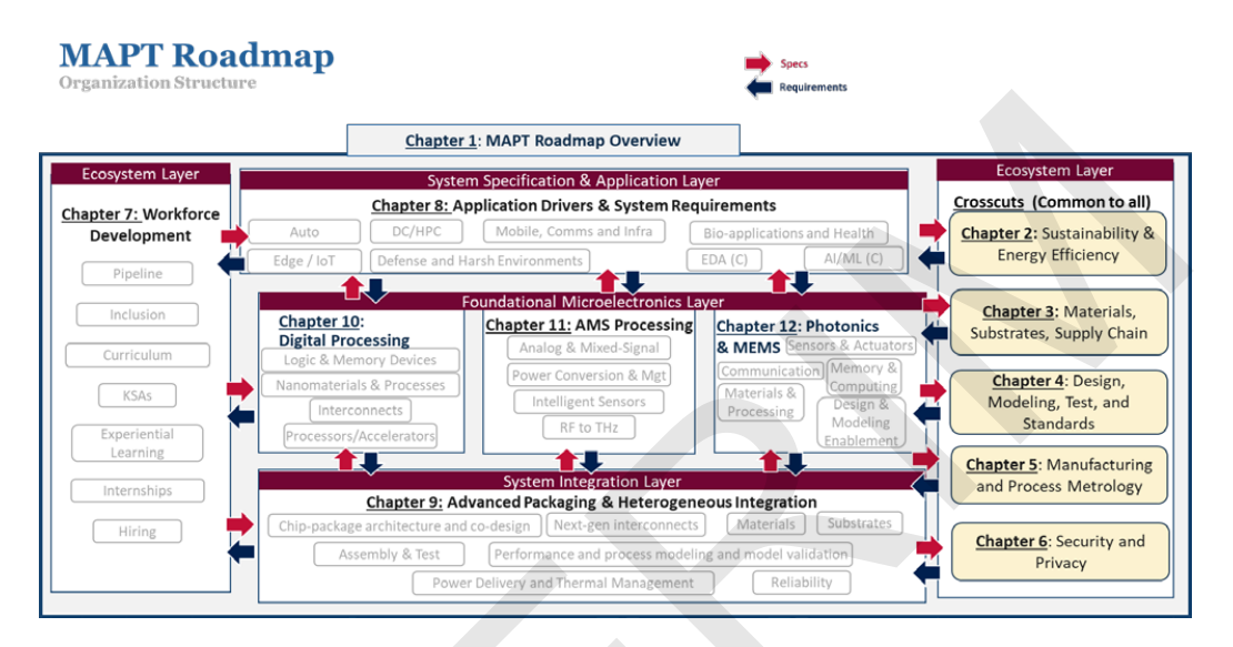
Image Generated Using Adobe Firefly
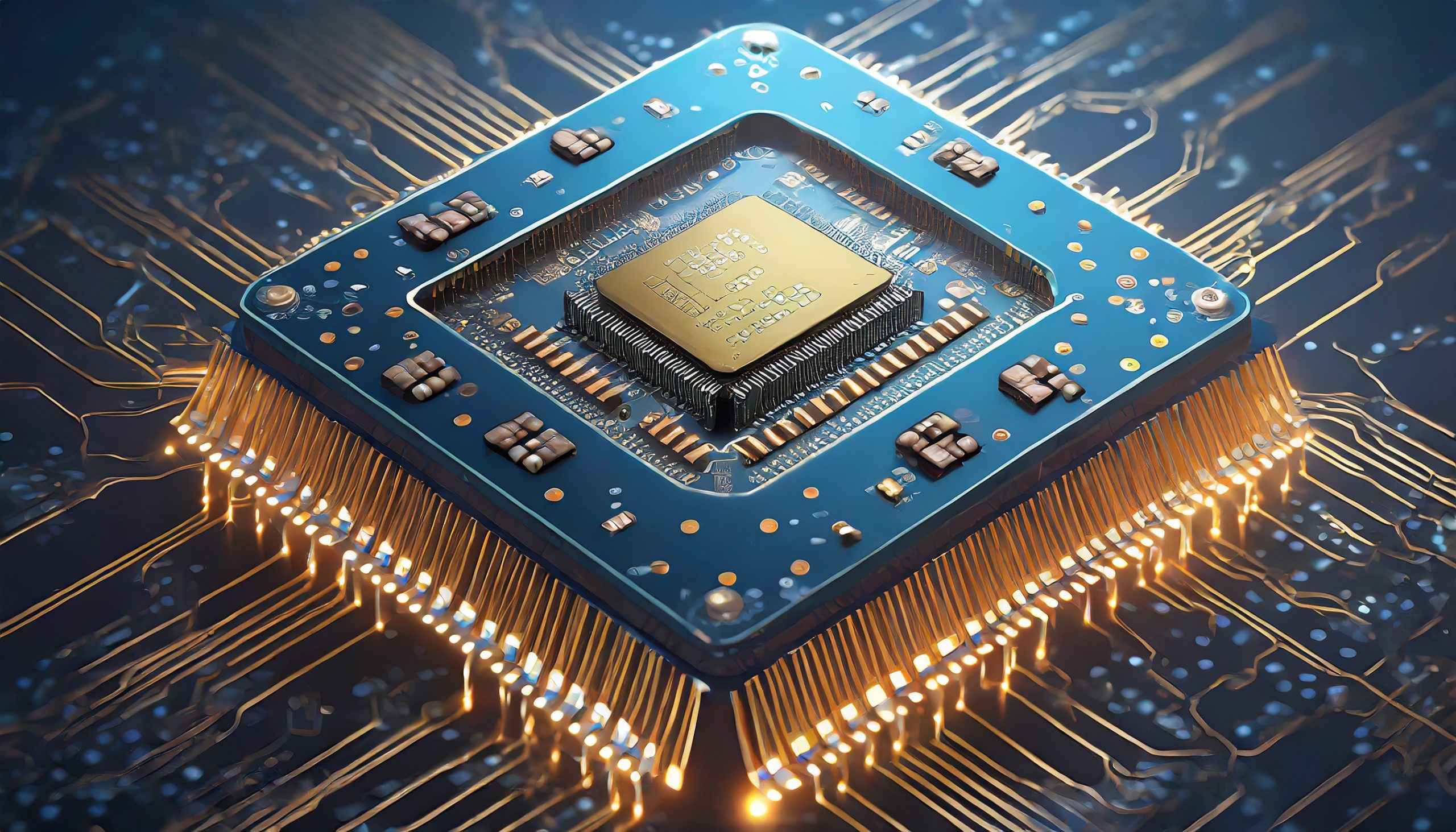
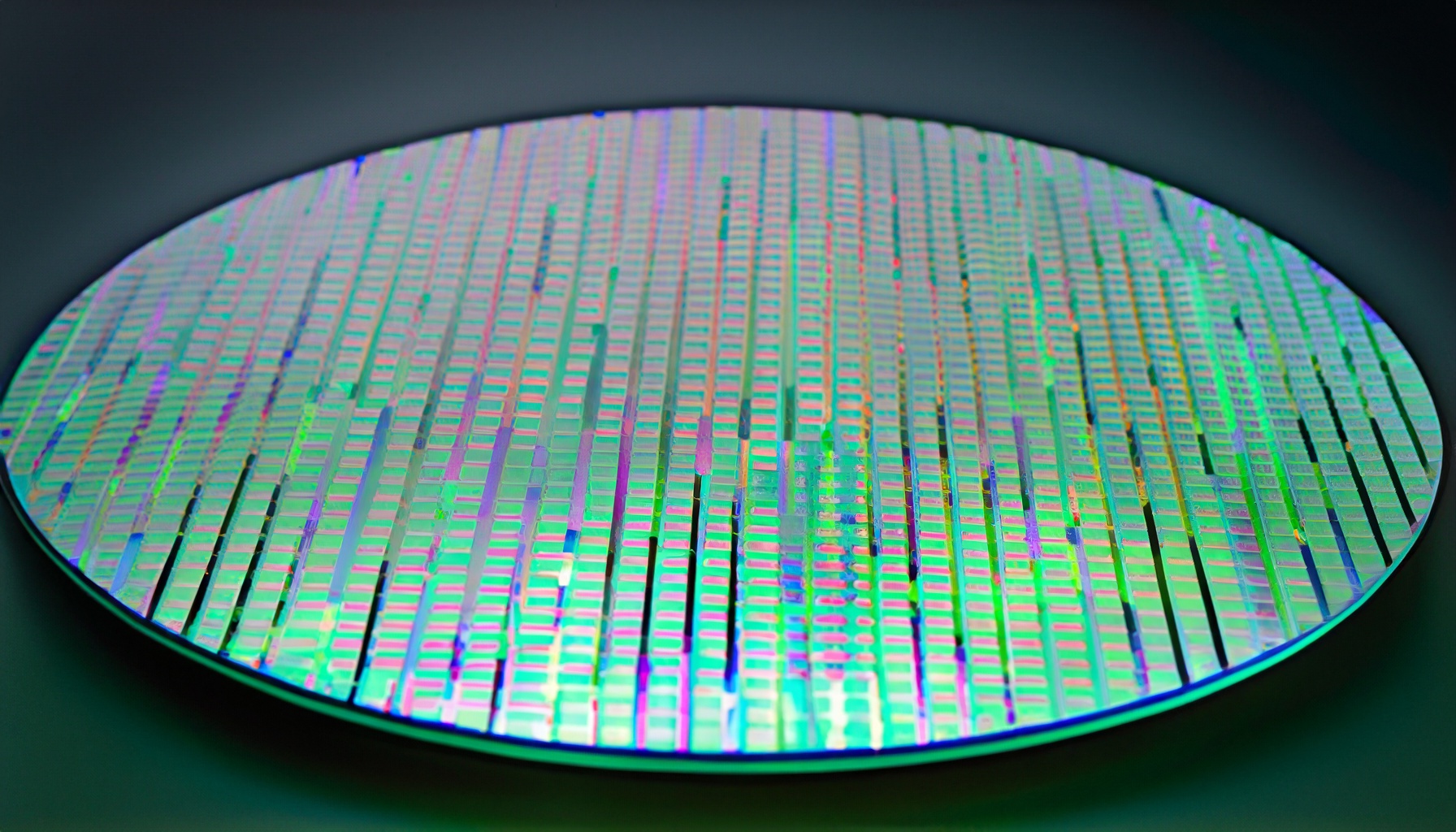
In semiconductor manufacturing, lithography is a pivotal process. It involves transferring circuit patterns onto a silicon wafer, a foundational step in creating integrated circuits (ICs).
Two of the most advanced lithography techniques currently at the forefront of this industry are Extreme Ultraviolet (EUV) and Nanoimprint Lithography (NIL).
Nanoimprint Lithography (NIL) and Extreme Ultraviolet Lithography (EUV) are two technologies used in semiconductor fabrication, each with advantages and challenges. Below is a comparative analysis.
Extreme Ultraviolet Lithography (EUV):
Technical Overview: EUV lithography employs a highly sophisticated process that uses extreme ultraviolet light (with a wavelength of approximately 13.5 nm) to etch wonderful patterns onto silicon wafers. This technology is a leap from traditional lithography, which uses deep ultraviolet light.
Advantages: The primary benefit of EUV is its unparalleled resolution, allowing for the production of smaller, more complex ICs. It is crucial as the industry moves towards ever-smaller node sizes, particularly 5nm and below. EUV enables higher circuit density, contributing to the chips’ enhanced performance and energy efficiency.
Challenges And Limitations: The transition to EUV has faced significant technical and financial difficulties. The development of EUV machines, such as those produced by ASML, is incredibly costly and complex. Furthermore, EUV requires highly purified materials and controlled environments to minimize photon absorption by air or contaminants. The technology also faces throughput limitations, as EUV processes are generally slower than their deep UV counterparts.
Nanoimprint Lithography (NIL):
Technical Overview: NIL is a form of lithography that physically imprints a pattern onto a substrate using a mold or stamp. This method is similar to traditional printing techniques but at a nanometer scale.
Advantages: NIL’s main advantage lies in its simplicity and cost-effectiveness compared to EUV. It can achieve high-resolution patterns without complex light sources or optics. NIL is particularly promising for applications that require large-area patterning, such as advanced sensors and display technologies.
Challenges And Limitations: NIL’s primary challenge is defectivity and uniformity over large areas. The physical nature of the imprinting process makes it susceptible to defects caused by particle contamination or imperfections in the mold. Maintaining uniform pressure and temperature across the entire wafer during imprinting is a significant challenge.

Comparative Analysis:
Resolution And Precision: While both techniques aim to push the boundaries of miniaturization, EUV currently leads in terms of resolution and is more suited for the most advanced logic and memory devices.
Throughput And Cost: NIL offers potentially higher throughput at a lower cost, making it an attractive option for specific semiconductor applications, particularly those not requiring the extreme miniaturization capabilities of EUV.
Application Suitability: EUV is helpful for high-end, cutting-edge semiconductor fabrication, especially for CPUs and GPUs. On the other hand, NIL finds its niche in less critical layers of ICs and in specialized applications like photonics and biochips.
The race between EUV and NIL is not a straightforward competition but rather a complementarity of technologies, each serving unique semiconductor market segments. As the industry progresses, we may see advancements in both technologies, potentially leading to hybrid approaches or innovations entirely. The choice between EUV and NIL will depend on specific application requirements, cost constraints, and technological advancements.
As the semiconductor industry continues to evolve, staying abreast of these developments is crucial for manufacturers, technologists, and stakeholders in this dynamic field.