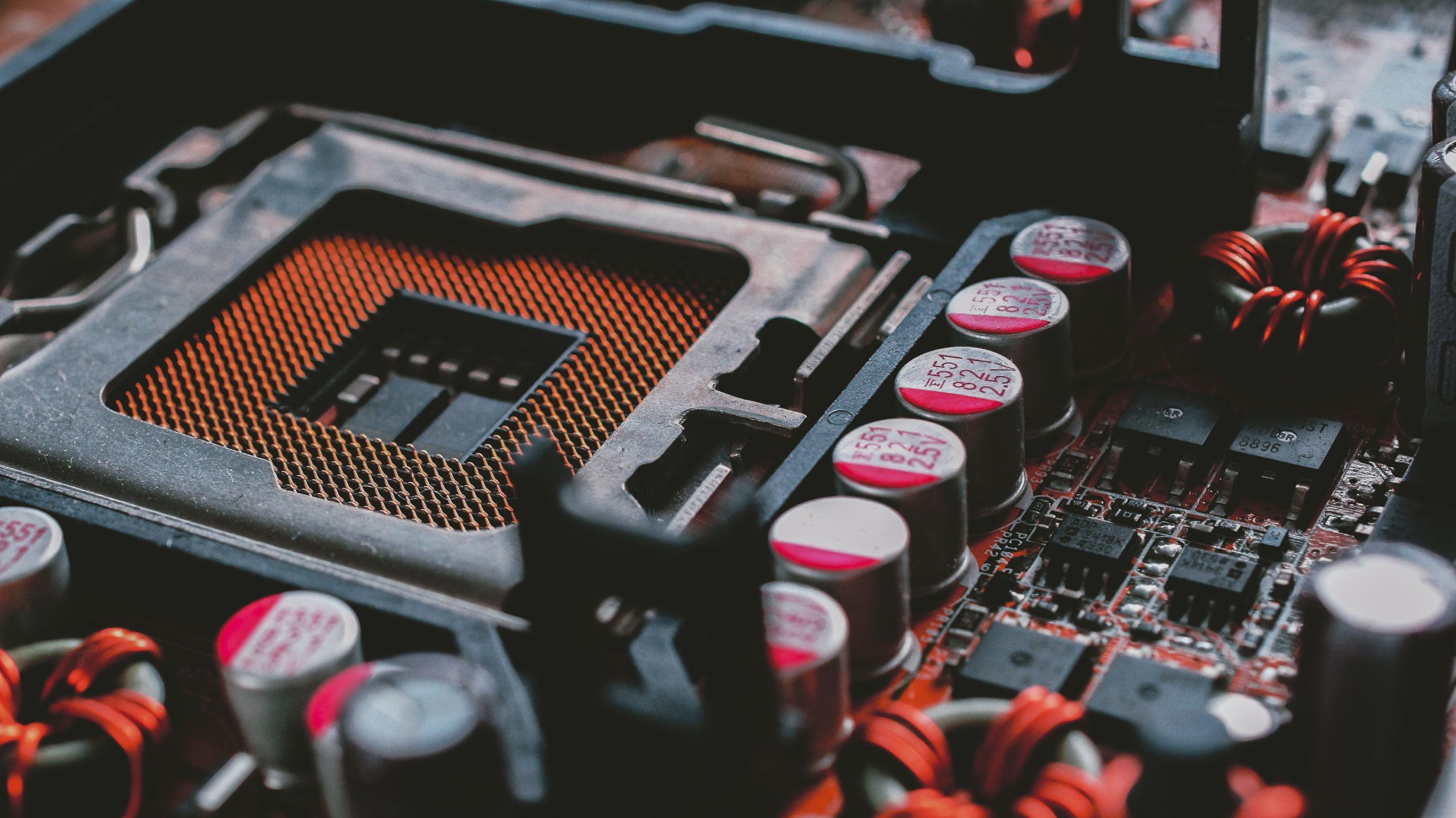
Photo by Maxence Pira on Unsplash
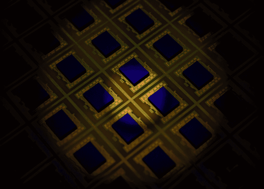
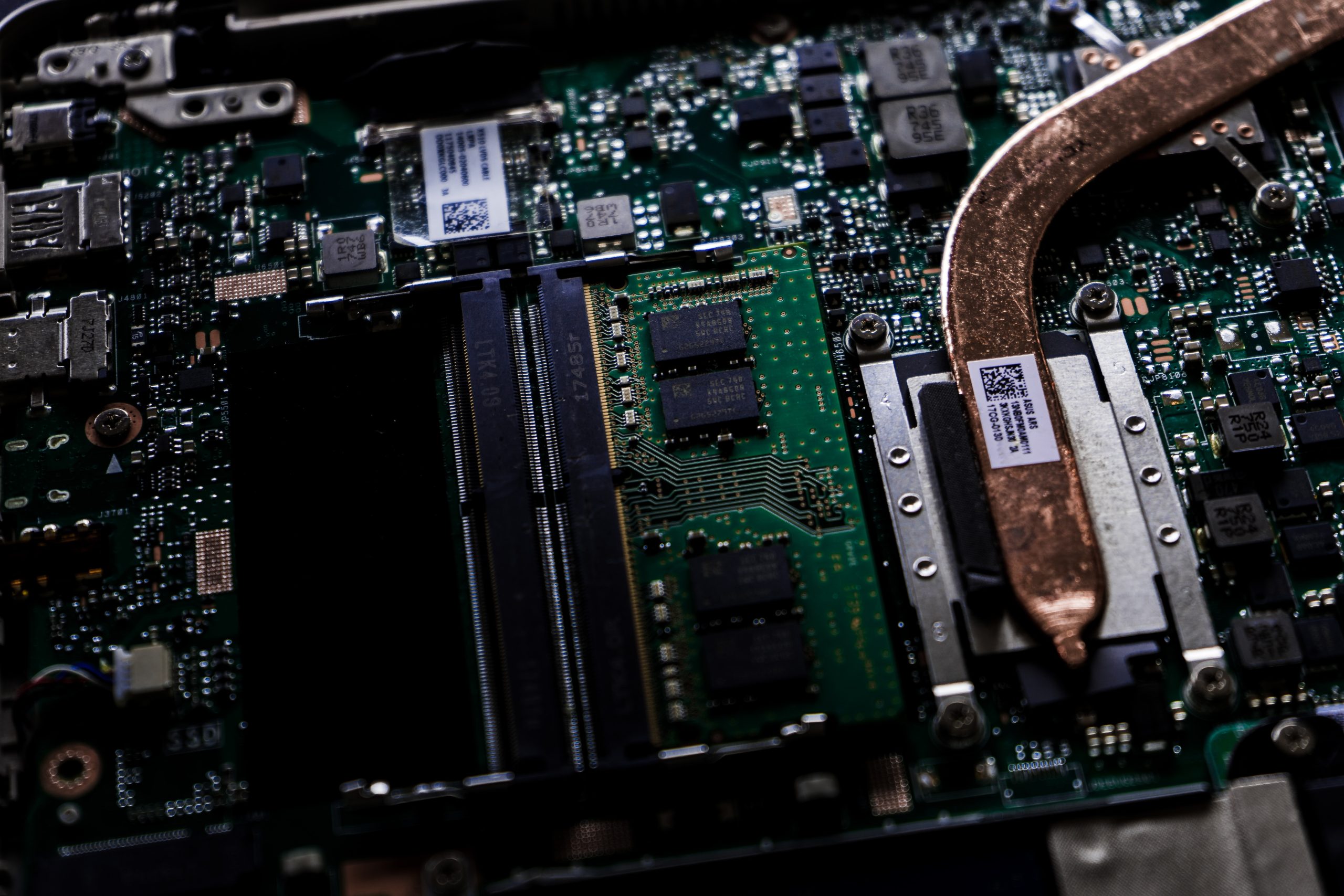
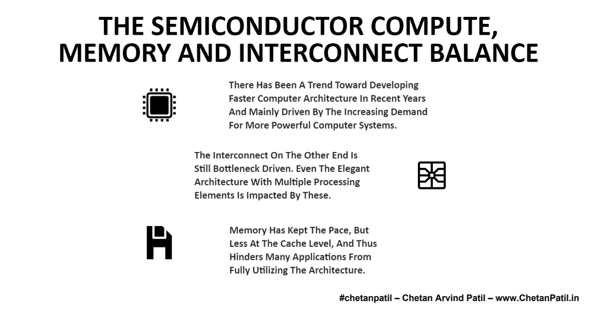
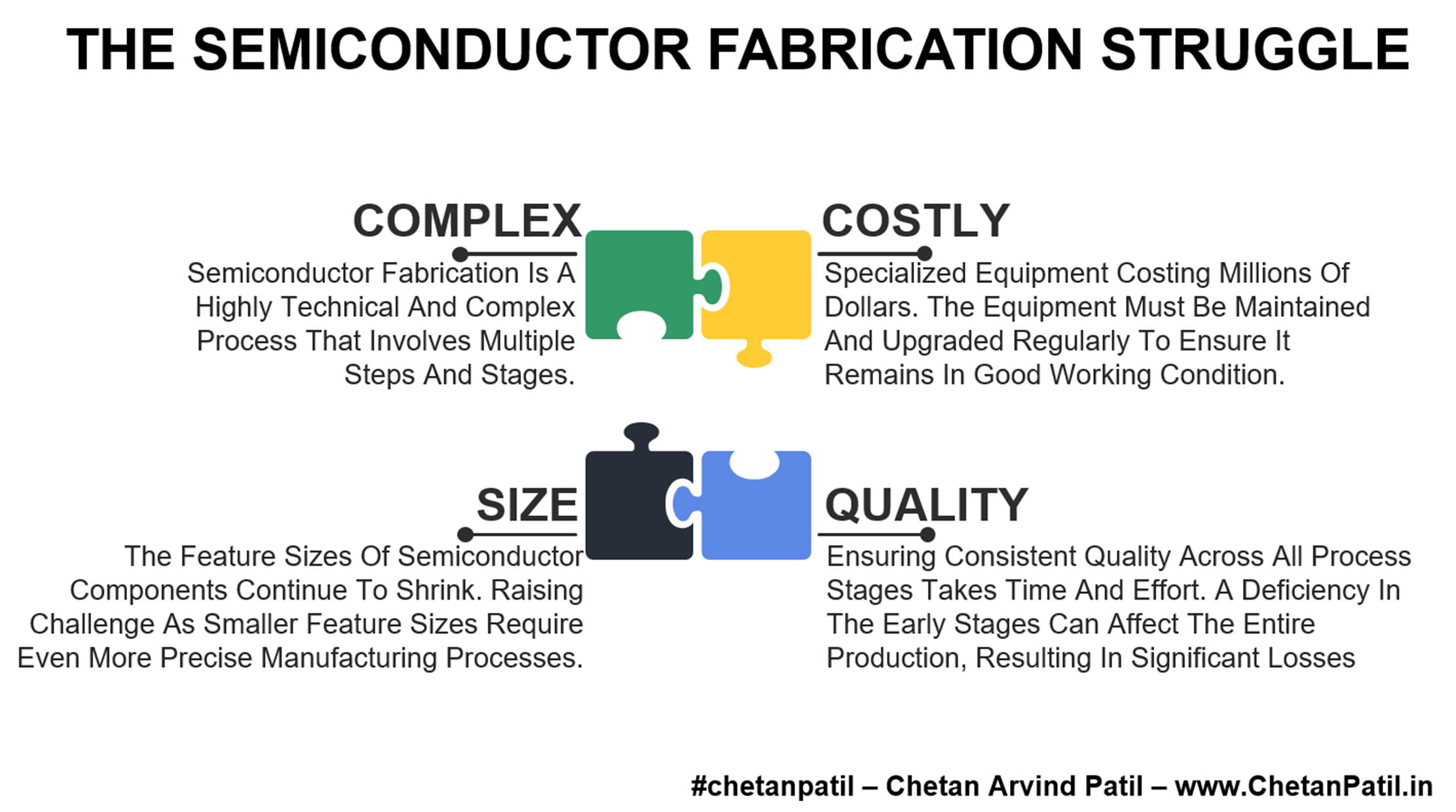
The semiconductor industry continually faces challenges as it shrinks transistor sizes to increase performance. One promising solution to achieve this goal is the use of chiplets. Chiplet is small; independent silicon dies that can be interconnected to create a larger, more powerful chip – chiplets.
Chiplets can provide several advantages over traditional monolithic chips, are customizable to meet the specific needs of a particular application, and can also be fabricated using different types of silicon nodes, which can reduce costs and improve performance.
Connect: High-Speed Interconnects Between The Chiplet And Chiplets Is A Major Hurdle.
Adoption: Takes Time For The Market To Adopt And Make It A Mainstream Solution.
However, there are also some critical hurdles that chiplets will need to overcome before they can become mainstream. One challenge is the need for high-speed interconnects between the chiplet and chiplets. These interconnect must handle the high data rates required by modern applications while being reliable and secure.
Another challenge is the need for a new design methodology for chiplets. Traditional chip design methods must be better suited for chiplets. New techniques must adhere to the requirements of several semiconductor companies trying to adopt chiplets to develop a disaggregated approach.
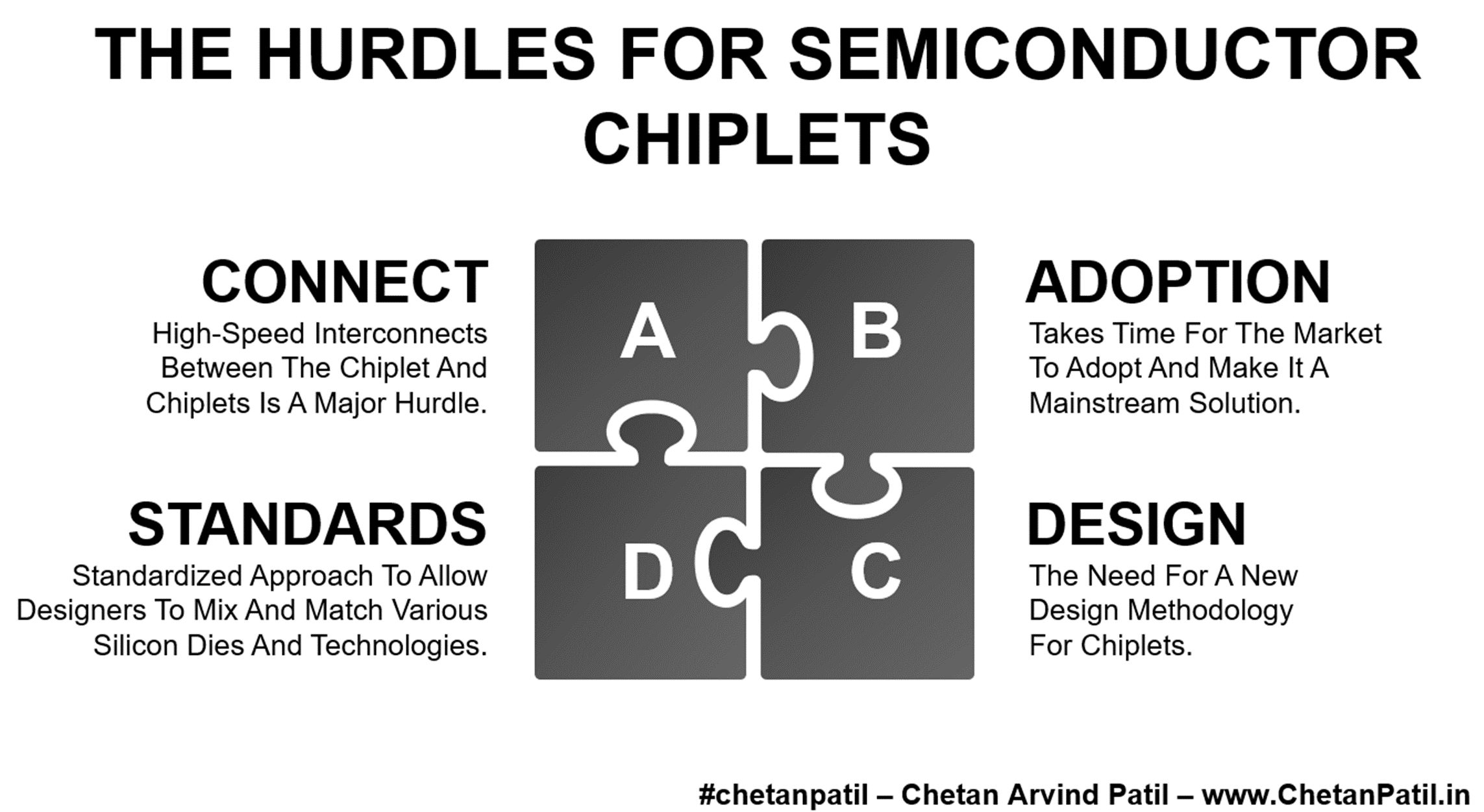
Market adoption is also a hurdle for chiplets as new design and manufacturing technology. It will take time for the market to adopt and make it a mainstream solution.
Despite these challenges, chiplets have the potential to revolutionize the semiconductor industry. They offer several advantages over traditional monolithic chips and could help address the industry’s challenges.
Design: The Need For A New Design Methodology For Chiplets.
Standards: Standardized Approach To Allow Designers To Mix And Match Various Silicon Dies And Technologies.
Chiplets can go a long way in addressing existing challenges, such as the rising cost of producing monolithic chips, and thus open the door to new, innovative chip designs. Eventually, by allowing designers to mix and match various silicon dies and technologies, chiplets can be used to create custom chips tailored to specific applications.
The future of chiplets is uncertain, but they have the potential to be a significant disruptive force in the semiconductor industry. Only time will tell if they can overcome their challenges and achieve widespread adoption.


@QHL6_DSCx7@5x.jpg)