Photo by Jason Leung on Unsplash
Artificial Intelligence (AI) driven by Machine Learning (ML) and Deep Learning (DL) has found its way into several industrial and consumer products. There is not a single high-tech solution that is not getting pitched as being AI-powered.
AI also requires a silicon platform that can enable the training of a vast set of data apart to form accurate predictions using models. It will not be wrong to say that AI adoption is dependent on how efficient and error-free the silicon platform is.
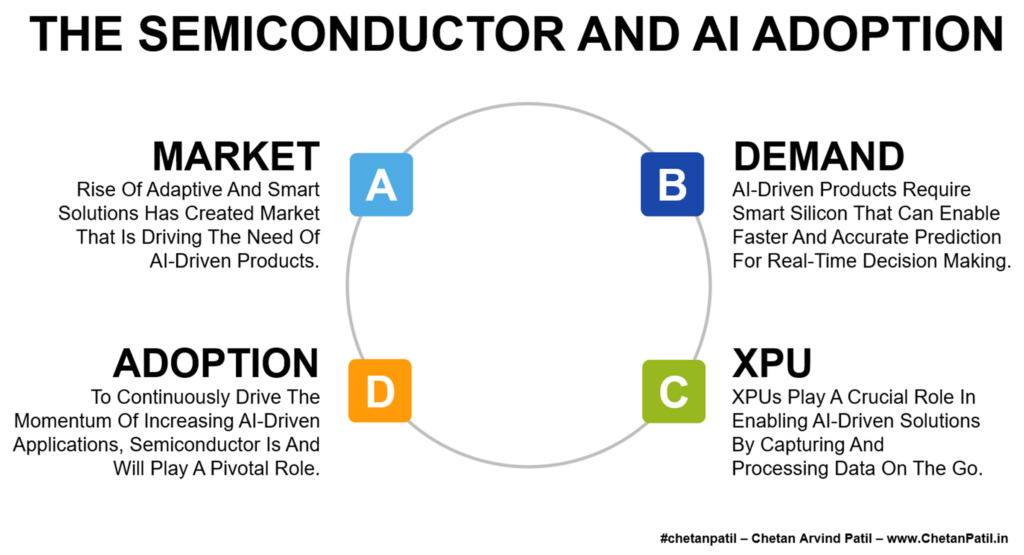
Market: AI-focused market is growing consistently and demands silicon that can enable faster decision making.
Demand: AI-driven solutions create the need for silicon that require advanced semiconductor technologies.
In 2022, there are already several AI-driven solutions utilizing the semiconductor capability to capture the market. Intel and AMD already have AI-focused XPUs that have enabled the computing industry to bring unique AI applications and services. Data-focused companies like Google, Amazon, and Microsoft have also spent years developing AI to help them understand consumer behavior faster than ever.
The AI-driven market and the demand for silicon that can power such a solution will keep growing, this, in turn, will drive the need for more efficient XPUs.
Several emerging companies are focused on providing specialized XPU that can enable adaptive decision-making on the go. AlphaICs, Alphawave, Cambricon Technologies, Graphcore, and Groq are some examples. All of these are focused on creating a unique silicon platform to speed up the adoption of AI.
Both enterprise and consumer markets demand AI-powered silicon that can cut down the cost and time to bring a new application to the market. As more consumers come online, the need for AI silicon will increase, and companies with the most bottleneck-free XPU solution will win the race.
XPU: The demand for AI applications requires a silicon platform that can drive bottleneck data processing.
Adoption: Smart silicon has already changed the AI race. As more elegant XPU silicon comes out, the adoption of AI-powered solutions will grow further.
The semiconductor industry is already marching with advanced technology nodes and chiplets-driven advanced package technologies. Such advanced manufacturing solutions are perfect for powering next-gen AI chips. However, the cost and capital required to enable such a solution are very high. Thus the strategy to bring up the manufacturing capacity of advanced nodes for the AI world should be more robust than ever.
The computing and semiconductor industries go hand in hand. As the need for consumer and enterprise-level AI-powered solutions grows, the adoption of AI chips will too, and semiconductors will (already are) play a pivotal role in decades to come.