Photo by Justin Luebke on Unsplash
The semiconductor industry is going through a wave of consolidation. It is not the first time the semiconductor industry is marching through such a wave. However, everyone time it does, it often has positive and negative impacts.
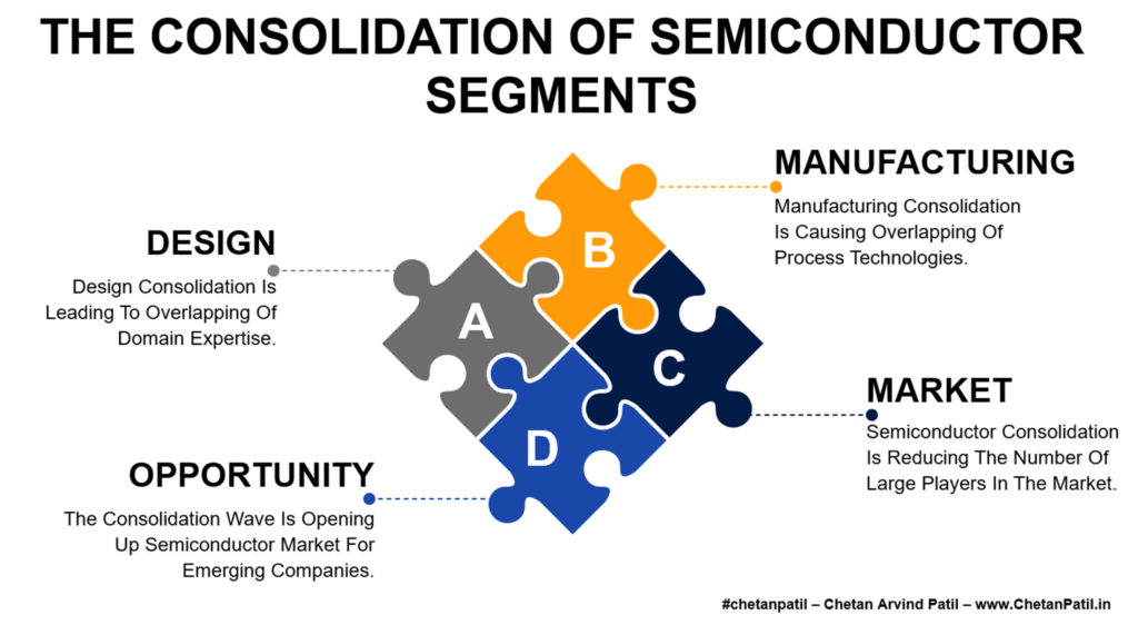
The reduction in the number of companies for a given semiconductor segment is one critical impact apart from the emergence of new players that try to create a new market that opened up due to the consolidation.
Top Players: Companies that have been in the semiconductor business for a long time either create new business to continue their presence in the market or get acquired (due to market volatility) by other companies, thus leading to consolidation of top players.
Small Players: When top players merge, there is a gap created in the market that opens up the opportunity for emerging players to focus and make the most of it. It is valid for solutions the old players are yet to find a stronghold on (RISC-V).
The ongoing semiconductor consolidation is across the design and manufacturing space. In the past, it was either design or manufacturing. It leads to a ripple effect across the semiconductor domains (memory to logic to nodes to packaging solution providers), which can go either (in terms of market demand) way for the semiconductor industry.
Design: Semiconductor companies that primarily focused on one solution (enterprise or consumer) are now entering new areas (wireless and automotive). It requires building teams from scratch or by merger and acquisition. Thus, creating a wave of consolidation.
Manufacturing: In semiconductor manufacturing, companies are entering a new arena to capture technologies that have not been their stronghold. The reason for such push is the need to enter a new market that does require some form of in-house manufacturing capacity.
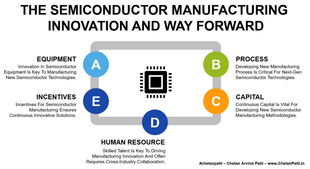
Eventually, consolidation might be a piece of good news and can push the semiconductor technology ahead at a faster pace. However, there are downsides when consolidations are not successful, mainly because it leads to the loss of time and investment.
The impact of consolidation within the semiconductor (from a design and manufacturing point of view) industry can be positive and negative.
The negative impact is when the number of players (companies) is reducing and thus creating less competition. It can also hinder the progress of new solutions. On another side, the positive impact can be the opportunities for emerging companies. They can create a market by leveraging the consolidation wave. One such example is utilizing RISC-V to create a new niche market to compete against x86/ARM (which is consolidating).
Market: Strong wave of consolidation reduces the number of top players, and it can have a negative impact due to the decreasing number of options for consumers and enterprises.
Opportunity: Semiconductor consolidation can also open up the market for emerging players, who can potentially grab new opportunities (and create a new market) due to the void created by the mergers and acquisitions.
The semiconductor consolidation wave thus has both positive and negative sides. It can shrink the segment by reducing the number of players, and on another side, it can open up opportunities for emerging players. In the long run, the semiconductor consolidation (in a majority of the scenario) pushes the industry forward.