Semiconductor wafers are fabricated and assembled to produce packaged semiconductor products before it gets shipped to customers. In the production, silicon product then gets mounted onto a system platform.
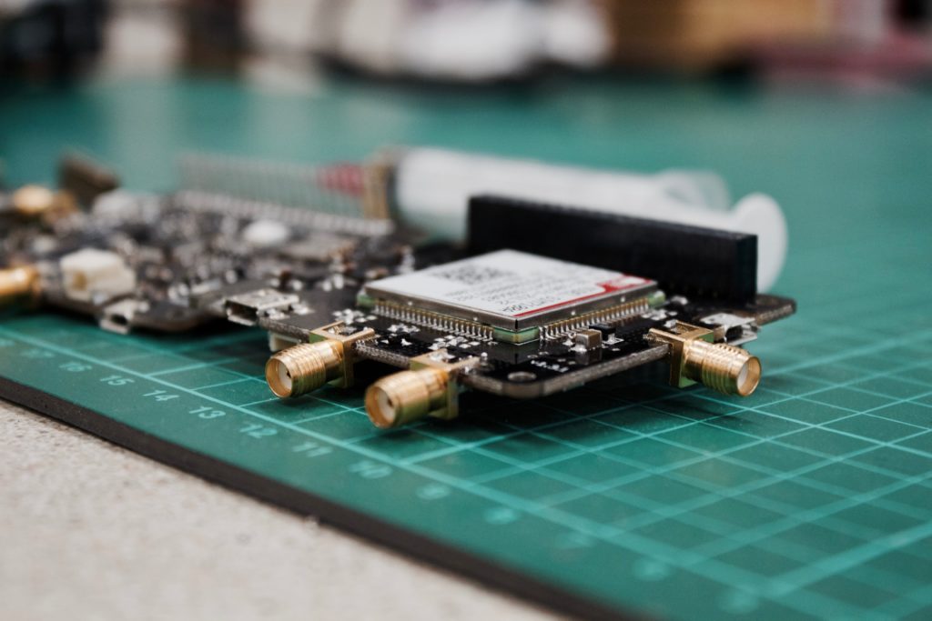
However, before the production line can use a semiconductor product, it needs to undergo several checks, which require a system-level platform calleda development board.
Development Board is a printed circuit board containing the main semiconductor product to be evaluated along with different support components needed to enable users to capture internal and external features of the target product.
Those interested in specific semiconductor products rely on the development board to thoroughly evaluate the capabilities of the silicon. Development board also provide a platform to electronic enthusiast and empowers them with options to test and build different semiconductor driven solutions. The Development board also ensures that the customer can capture the capabilities as promised in the datasheet.
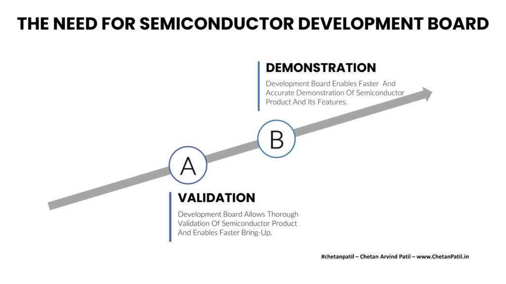
Validation: Validation is the base requirement of any semiconductor product, and the development board provides such an option. Validation ensures that the product works as per the specifications, and it requires the semiconductor product to get mounted onto the development board. Doing so provides avenues to the customer to validate the end product.
Demonstration: Development board enables a platform to drive different demos. These demos give a quick evaluation of how the semiconductor product can develop next-gen solutions. During the consumer electronic exhibition, the development boards play a role by enabling demo of features that can potentially attract new customers.
Not all development boards get designed for the mass market. Several are for a specific purpose and used by the semiconductor design company and their customer only. Development boards for the mass market (Arduino, Raspberry, etc.) have been around for years and have always enabled new ideas.
In the end, the development board needs to have an impact on the end-user. It is only possible based on how good the development board is for evaluation purposes.
The impact the development board has on the semiconductor product defines how good the platforms can be. Not all products need a development board, but those which do should equip end-user with options to investigate the semiconductor product under evaluation.
Several criteria can define how impactful the semiconductor development board is. Eventually, it all boils down to a couple of critical features that decide whether the development board can provide the much-needed hooks to capture end-to-end features.
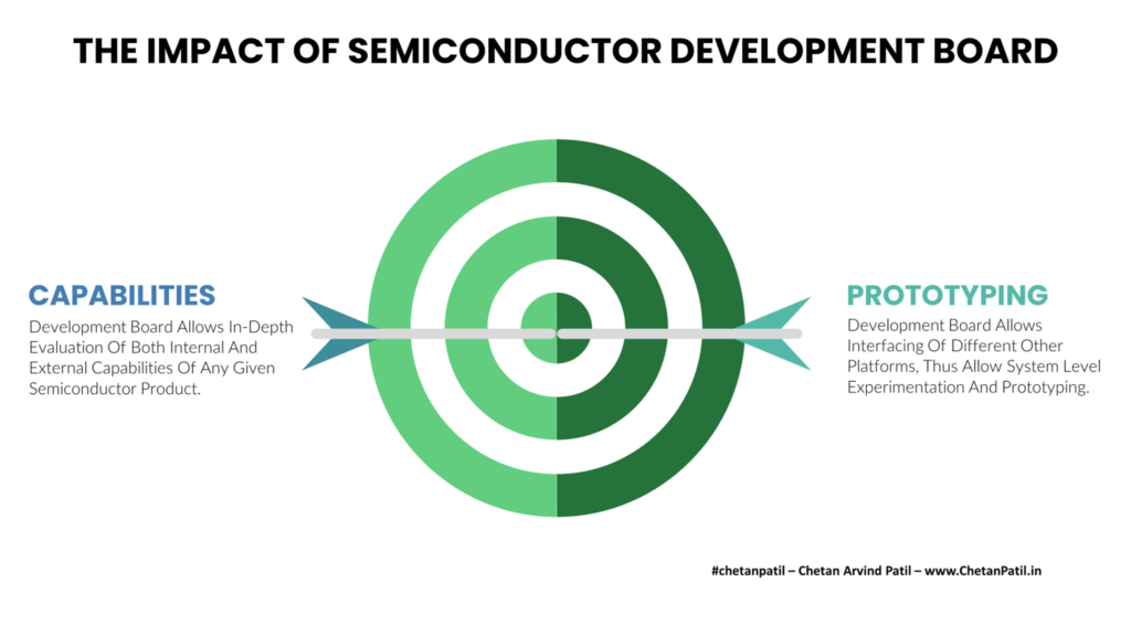
Capabilities: A development board provides a detailed evaluation of the semiconductor product’s capabilities, and to capture all the features, it is crucial to provide all the necessary support files, guides, software, tutorials, and other details. Otherwise, the impact of the semiconductor product from its capabilities will be next to none.
Prototyping: All development boards have to comes up with features to drive prototyping. It requires the development board to come with peripherals that allow connection or communication to the next platform. Empowering prototyping also enables the testing of new and innovative ideas. Thus, the impact development boards have from prototyping is crucial too.
The main goal of development is to showcase the system-level capabilities, and it requires several other components to get mounted on the same target development platform. In the end, it becomes the evaluation of several semiconductor products, not just one. And, such an evaluation process is crucial as any production line always requires more than one silicon component to work together.
As several new semiconductor products (mainly on the processor and wireless communication side) come out in the market, the need for development boards will keep growing. New development boards with new semiconductor products also mean new options for the semiconductor market.
The computing world is heavily reliant on semiconductor products. To implement target features, it is important to look into the low-level hardware characteristics. These characteristics over the years have become key driving factors and are not defining how future semiconductor-powered computing will be.
The features that drive semiconductor computing are well known. These are a perfect combination of technical and business aspects. The business aspect focuses on increasing the margin apart from acquiring new markets and customers. The technical features set the foundation of how the computing system will work.
The technical and business feature list is endless, but below few points define how key features drive the semiconductor-powered computing world.
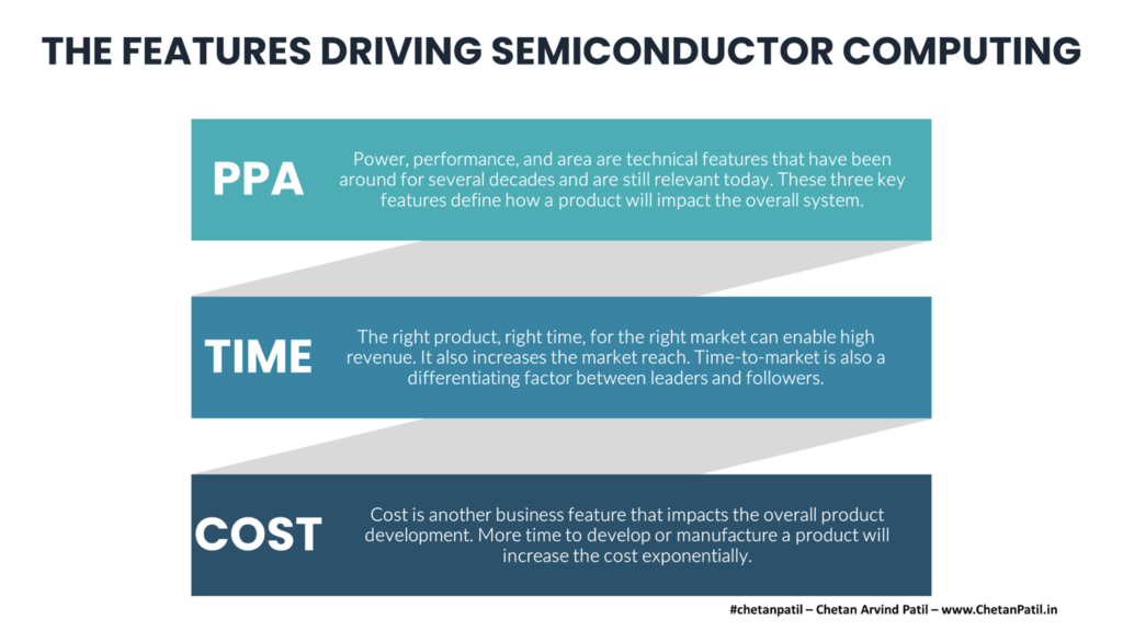
PPA: Power, performance, and area are technical features that have been around for several decades and are still relevant today. These three key features define how a product will impact the overall system. As semiconductor technology has progressed, these three features have too. In the end, it all boils down to the different combinations of these three factors, which are required to power any given semiconductor computing system.
Time: Time is a business feature, and it tracks the time required to bring the product into the market. The right product, right time, for the right market can enable high revenue. It also increases the market reach. In a highly competitive world like the semiconductor industry, the time has been a differentiating factor between leaders and followers.
Cost: Cost is another business feature that impacts the overall product development. More time to develop or manufacture a product will increase the cost exponentially. New semiconductor technologies like FETs, Packaging, and Testing also have increased the cost of product development.
Two critical changes have occurred in approximately the last two years: First is the increasing complexityof the semiconductor products that power the computing world (XPUs etc.). Secondis the resources required to bring the complex features into the market.
The complexity comes as part of providing modern features. The resources aspect (non-human) is something that has an impact on semiconductor computing. The reason is the CapEx-driven facilities and continuous investment required to drive next-gen semiconductor computing.
The world of computing is advancing. The need to provide modern semiconductor-powered systems is never going to end. To meet customer (and market) demand, the semiconductor industry has to keep inventing next-gen features.
The semiconductor industry has already been inventing new technologies for decades and thus pushing the computing industry forward. These features have followed Moore’s law, and several got launched due to the market demand.
FET: FETs are the building blocks of any silicon chip. Several transformational changes have occurred around FETs. However, the angstrom era demands a new wave of FETs that can drive the critical components (XPUs and other similar chips) towards power and performance needs that can drive next-gen semiconductor needs. These can be from better operating to area requirements.
Package: Like FETs, package technology has to evolve. While several advanced packaging solutions already exist, there are still new features required to manage the complexity of the new generation of design methodologies like chiplets brings-in. On top of all this, package technology also has to be cost-effective, otherwise, the cost of manufacturing will keep rising.
Adaptive: Workloads are getting complex year-on-year. Constant architecture processing these new workloads often ends up with bottlenecks. Design and manufacturing approaches for chips targeted for the computing industry needs to be more adaptive. Neural Processing Units (NPUs) provide a way forward, but still, a lot of work is required to make it mass-market friendly.
The computing world is going through drastic changes. Customers want a balance of power and performance to drive savings without impacting features. Balancing these two features is not an easy task. That is why next-gen features like FETs, package technologies, and adaptive will play a key role in shaping up the semiconductor-powered computing industry for the decades to come.
Apart from features, drastic changes in design and manufacturing methodologies are also two key pieces that will drive next-gen semiconductor computing features. All this will heavily rely on how the existing and emerging semiconductor companies bring in the new solutions.
The semiconductor design and manufacturing business are highly competitive. As semiconductor design and manufacturing companies compete to increase their market share, a flawless strategy is required.
However, achieving perfection in the semiconductor business requires several different factors to come together. The competing process is one such factor. It is vital to focus on the process of competing because it can make or break the future of any given semiconductor company. A lack of focus on the capabilities can push the company towards a course of action that can negatively impact the market share and thus the revenue.
Semiconductor companies often have a lot of overlapping business areas. Thus, solutions from one company might well be the driving factor of the product from different companies. For example, a company focused on XPU business requires companies that provide silicon to enable communication solutions. Without each of these (and several other) products, the system will be incomplete.
It leaves the semiconductor companies to march towards two processes of expanding market share: Either compete or cooperate. A semiconductor is a business where the success of one product drives the other (XPU driving Wireless adoption as discussed above), and that is why semiconductor companies should focus more on the cooperative competition: coopetition.
Competition: Multiple companies are competing to launch products to increase their market share.
Coopetition: Two or more companies form a strategic alliance or JV to drive the development of each other and thus creating a market for all.
Coopetition is not a new concept and has been around for decades. Given that the semiconductor business (year on year) is becoming highly CapEx-driven, it makes more sense to drive the environment of coopetition than the competition.
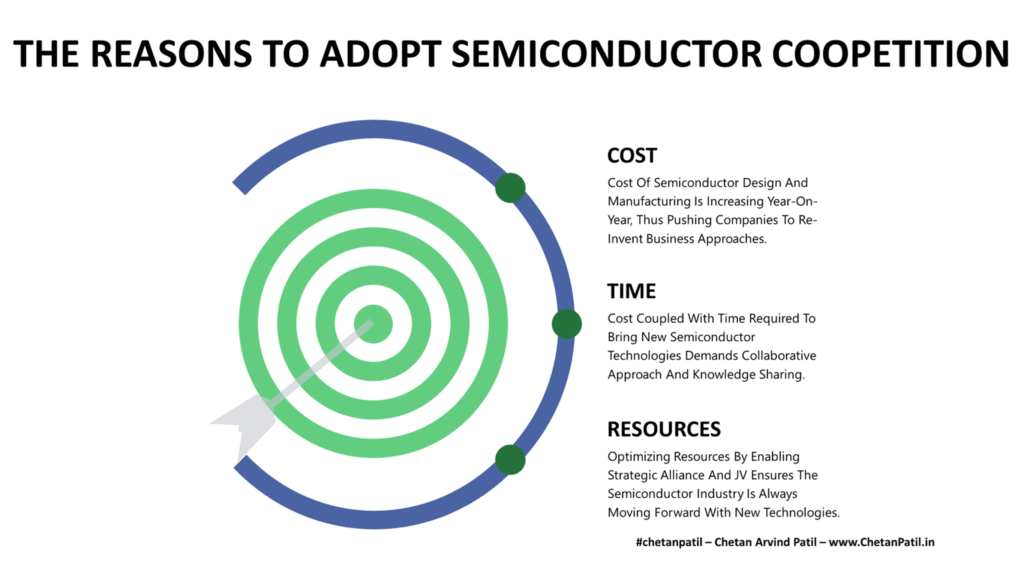
Cost: High cost to design next-gen solutions (driven by resources, lab investment, and equipment) has pushed semiconductor companies to innovate on how they compete because competition means launching products ahead of the competitor (and with far better features). Doing so requires continuous investment and impacts the margin, thus raising questions as to whether coopetition is the way forward.
Time: Cooperative process reduces the time to develop new IPs (and other solutions). And it can benefit all the parties working together. One such example is the alliance around USB and Wi-Fi specifications, which enabled several companies to launch new products while keeping the base features intact. Cooperative competition pushes the semiconductor industry towards a time-sensitive process.
Resources: Strategic alliance/JV via coopetition ensures that the technical resources of all the parties get utilized efficiently. It also enables knowledge sharing, which speeds the process of innovation and thus ensures that resources drive the innovation required to increase the market base.
The benefits of competition are not only on the business side but also on the technical side. Knowledge sharing enables new semiconductor technologies, both on the design and the manufacturing side, and drives the industry towards next-gen solutions.
In the long run, the cooperative competition presents more new opportunities wherein multiple semiconductor businesses can thrive and drive each other’s business. It is also evident from the fact that any given computing system requires solutions from different semiconductor companies.
A competitive environment in a high-tech industry like the semiconductor industry always demands innovative business strategies apart from technical roadmaps. Thus, competing without cooperation might lead to a path that is not business-friendly.
On another side, cooperative competition (coopetition) has its benefits. It allows everyone to thrive and also enables several new benefits. It includes entry into new markets, opening a new revenue stream, and several other benefits. These and several other reasons are why the semiconductor industry should march towards (and already has) a coopetition environment.
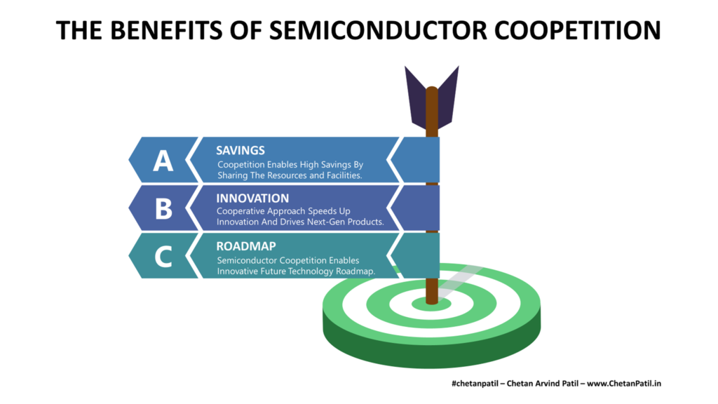
Savings: Sharing facilities and technical knowledge imply saving time to innovate. It directly reduces the cost and ensures that semiconductor companies are more profitable without compromising the product features.
Innovation: Game-changing innovation requires strategic alliance not only with academia but also with industry peers. A coopetition process enables such an environment and thus ensures all the players involved are thriving by utilizing the innovation developed by the cooperative process.
Roadmap: Focusing on the technology roadmap without collaborating might lead to solutions that may not pay back in the long run. Approaching the same process by utilizing the coopetition process ensures that the roadmap developed helps the industry. It can be developing technologies that drive manufacturing to new levels or creating devices/FETs that push new innovative solutions from design houses too.
The semiconductor industry has already seen several positive coopetition examples wherein companies have collaborated to drive the business of each other. Mobile to the server to automotive and several other areas would not exist without a coopetition environment. Each of this business relies heavily on semiconductor products and have to collaborate to drive next-gen systems.
The growing cost and the need to balance the margin (coupled with different other problems) makes the case of driving the coopetition ecosystem. In the end, it is only going to benefit the semiconductor industry.
Benchmarking a product is one of the most common evaluation processes, and from software to hardware, benchmarking is extensively used.
In the semiconductor industry, benchmarking is mainly used to evaluate products against their predecessors and also competitors. CPU and GPU get benchmarked more often than any other type of silicon product, and the reason is the heavy dependence on day-to-day computing on these two types of processing units.
Benchmarking: Capturing technical characteristics and comparing them against other reference products to showcase where the new product stands.
Comparing one semiconductor product with another or old one is one of the reasons to benchmark. Benchmarking enables several key data points and makes the decision-making process easier for end customers. In many cases, it also pushes the competitors to launch new products.
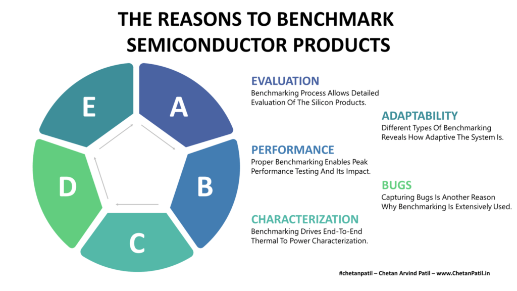
Evaluation: Benchmarking provides a path to unravel all the internal features of a new semiconductor product. Evaluating products using different workloads presents a clear technical picture of device capabilities.
Performance: The majority of the semiconductor products get designed to balance power and performance, while several are also focused purely on peak performance without considering the power consumption. Either way, executing the benchmarking workload on a silicon product allows capturing of detailed performance characteristics.
Characterization: Power, performance, voltage, and time are few technical data points that enable characterization. Benchmarking tools are capable of capturing these details by stressing the product with different operating conditions. Such data point provides a way to capture the capabilities of a product over different settings.
Bugs: Stressing a product using different benchmarking workloads can reveal if there are bugs in the product. Bugs are captured based on whether the benchmarking criteria are leading to expected data as per the specification. If not, then designers and manufacturers can revisit the development stage to fix the issue.
Adaptability:Benchmarking also provides a path to capture how adaptive the semiconductor product is. It can be done by simple experiments wherein the product is stressed using benchmarking workloads under different temperature to voltage settings. Any failure or deviating results during such benchmarking can provide a way to capture and correct issues before mass production.
Benchmarking also reveals several data points to the buyers and empowers them with information about why a specific new product is better than the other. Relying on benchmarking process has become a norm in the computing industry. It is also why any new semiconductor product launch (CPU or GPU) comes loaded with benchmarking data.
With several new semiconductor products coming out in the marking and catering to different domains (wireless, sensor, computing, and many more), benchmarking presents a way to capture the true potential of the new product.
However, correctly executing a benchmarking process is critical, and any mistake can present a false impression about the product getting evaluated. Hence it is vital to benchmark a product correctly.
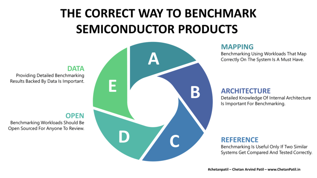
THE CORRECT WAY TO BENCHMARK SEMICONDUCTOR PRODUCTS
Benchmarking semiconductor products like XPU (and several others) is not an easy task. It requires detailed knowledge of internal features to ensure the workload used for benchmarking is correctly utilizing all the new embedded features.
A false benchmarking process can make or break a product, and it can also invite several questions on any previous product that used a similar benchmarking process. To correctly benchmark a product requires covering several unique points so that all the features get evaluated.
Mapping: The benchmarking world has several workloads. However, not all are designed and then tested by correctly mapping the software on top of the hardware. For correct benchmarking, it is critical to capture all the features that enable the correct overlay of the workload on top of the silicon product. Doing so ensures that the benchmarking workload can take benefits of all the internal architectural features before.
Architecture: Understanding different features and architectural optimization is a vital part of correctly benchmarking the products. There are generic benchmarking tools and workloads, but not all can take advantage of all the register level techniques to optimize the data flow. A good understanding (which also requires detailed documentation from the semiconductor company) of architecture is necessary before any benchmarking is executed. This also enables a fair comparison without overlooking any features.
Reference: The major goal of benchmarking is to showcase how good the new product is. To showcase such results require a reference, which can be a predecessor product from the same company or a competitor. Without a reference data point, there is no value in positive benchmarking results. Hence, having as many references benchmarking data points as possible is a good way to compare results.
Open: To drive fair benchmarking, open-sourcing the software (workloads) code can instill a high level of confidence in the results. The open process also allows code contribution, which can improve the workloads, and thus the benchmarking results will be more reliable than ever.
Data:Sharing as much benchmarking data as possible is also a good strategy. Peer review of the data points also improves the benchmarking process of future products. Historical benchmarking data points also drives contribution from data enthusiast and thus can help improve the benchmarking process and standardization.
Several tools and workloads are available to evaluate and benchmark a semiconductor product. However, the majority of these workloads/tools are written without 100% information about the internal features of any given product, which might lead to false-positive/negative benchmarking data points.
All this pushes the case for standardizing the benchmarking process so that any semiconductor product when compared against others (in the same domain), gets evaluated for set/standard data points. On top, as more complex XPUs and similar products (neuromorphic chips) come out in the market, standard benchmarking protocols will provide a way to correctly evaluate all the new technologies (and design solutions) that several old/emerging companies are launching.
Benchmarking is not a new process and has been around in the semiconductor industry for several decades, and it will be part of the semiconductor industry for decades to come. The only question is how fair the future benchmarking process will be.
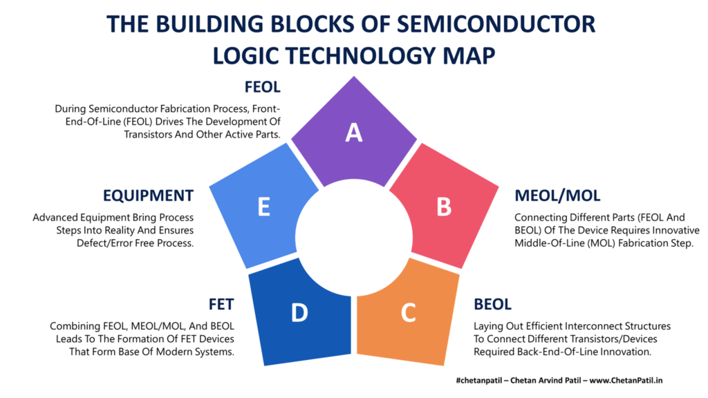
THE BUILDING BLOCKS OF SEMICONDUCTOR LOGIC TECHNOLOGY MAP
The transistor is one of the building blocks of the semiconductor industry. It has also gone through drastic transformation led by very high activity of research and development. These transformational changes, year on year, have empowered the semiconductor industry in providing solutions that are 2x faster and occupy 2x less space.
Optimization activities have not stopped, and now companies and academia are gearing up to target next-gen solutions that will drive the semiconductor solutions into the More-Than-Moore era. And, to drive next-gen transistors, different research entities (semiconductor FABs and FAB-LESS) must focus on a semiconductor logic technology map.
FAB/OSAT Map:Provides an overview of how semiconductor technology will progress within a given FAB and OSAT.
Logic Technology Map:Provides an overview of how the device/transistor level technology will progress to enable next-gen logic devices.
The sole goal of the semiconductor logic technology map is to come up with new ways to enhance transistors. Developments around semiconductor logic technology map are the reasons why today the semiconductor industry has seen different types of transistors: PlanarFET, FinFET, GAAFET, and now MBCFET.
FEOL: Front-End-Of-Line is the backbone of semiconductor devices. The way FEOL technology progresses drives the technical characteristics of the devices/transistors. Time to turn on/off without adding delay is also one of the focuses of FEOL devices. FABs are dependent on FEOL and often have to work relentlessly in ensuring the new process is improved correctly to bring new technology-node.
MEOL/MOL: Middle-End-Of-Line/Middle-Of-Line builds the connection between FEOL and BEOL, and acts as a catalyst by providing tiny structures that allow the pathway between the front and back end of the semiconductor device development. As the complexity of the transistors has increased, so has the process to create tiny structures between the front and the back end side. The complexity and the importance make MEOL/MOL a critical logic block.
BEOL: Back-End-Of-Line takes the help of different types of metal structures to provide an interconnect between different types of transistor devices. BEOL ensures that devices interact, and the chip is active and always working as per the design.
FET: Transistors development is tied to how FEOL, MEOL/MOL, and BEOL evolve. In the end, customers are focused on how the power, performance, and thermal profiles of next-gen FET transistors. Such key metrics can make or break the next-gen FET adoption. Given the dependence on FETs to enable the vision of building efficient products, FETs are one of the crucial blocks of the semiconductor logic technology map.
Equipment:It is not possible to drive the development of new semiconductor processes without advanced equipment. Semiconductor equipment manufacturers have to work closely with the FABs and research team focused on bringing next-gen FET. It ensures that the new equipment is capable of driving the vision into reality. In many cases, the pros and cons around the equipment technology (EUV) can decide the fate of whether the research/theory can be brought into reality or not.
Building blocks of semiconductor logic technology map ensures that the next-gen devices keep getting launched. Thus can also provide process-level solutions to the customers to make the most of their designs.
It is crucial for Pure-Play or IDM to come up with a clear long-term semiconductor logic technology map that can excite their customers and allow them to make most of their design from a power, performance, thermal, and operating voltage point of view.
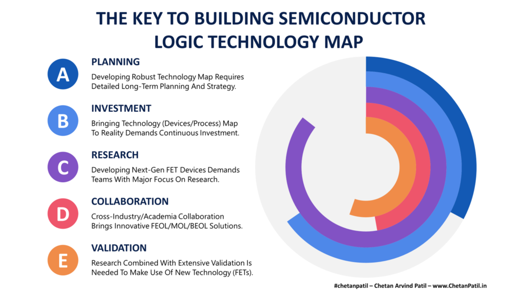
THE KEY TO BUILDING SEMICONDUCTOR LOGIC TECHNOLOGY MAP
The building blocks of the semiconductor logic technology map are well known to the majority of the industry. What sets a specific semiconductor entity apart is the resources required to drive the semiconductor logic technology map.
Research and development to enable next-gen logic solutions/transistors require long-term planning. It is also one of the most highly resource-demanding processes and takes years (even decades) to validate the theory.
To increase the success rate of such a long-term process, different semiconductor logic-focused stakeholders (academia and industry) need to drive key activities to build a robust semiconductor logic technology.
Planning: A long-term planning enables teams to focus on solutions that can bring efficient logic devices into the market. There are so many areas within the semiconductor fabrication process. Hence, it becomes critical to have a dedicated yearly (or five-year) plan to bring new devices into the market to ensure the customers understand how new solutions will drive future semiconductor products.
Investment: Planning requires investment, and it is critical to invest in specific resources that maximize outcomes. Whether forming technical teams or building new advanced labs with modern equipment, all require long-term continuous investment. Thus, investment (and that too continuous) towards the next-gen device is critical.
Research: Planning combined with investment can drive very high research activity. Research requires a dedicated academic team or a mix of industry and academia. In the end, the goal is to come up with logic-level solutions to ensure the next-gen device is more advanced than any of its predecessors. Hiring the right resources for logic research activities is crucial too.
Collaboration: Proper planning, investment, and research often require a collaborative approach. It can be cross-industry or cross-academia. Whichever path, the end goal is always to ensure the collaboration often leads to fruitful results. Collaboration is often a differentiating factor of all the highly advanced solutions in use today compared to those which didn’t end up getting used.
Validation: Planning combined with investment and research-driven by active collaboration is fruitful only if the theory is validated. The validation demands a dedicated facility (FABs, Labs, Equipment, etc.) that can drive the validation process to ensure the new logic solutions aligns with the theory. Lack of validation can break the years of research, and the validation process also enables customers to capture the pros/cons of new logic solutions.
Years and decades of shrinking transistor size have allowed the industry to provide new semiconductor products. To continue the momentum (beyond the angstrom era) of semiconductor logic technology map means bringing different key blocks to work together in harmony.
It takes years of effort to bring next-gen semiconductor logic solutions into the market. Then another few years to break even around the new proposed solutions. To ensure all such goals get achieved in a time-bound manner, semiconductor companies need to plan and openly share the logic technology map.
THE REASONS TO USE SEMICONDUCTOR CHIPLETS FOR MANY-CORE ARCHITECTURES
Computer architecture is a set of design steps that drives the manufacturing of innovative processing units, worldwide known as the processor. These processors follow the rules as defined by the computer architects and the end goal is always to process the data as fast as possible.
To make the next-gen processor efficient than today’s, computer architects focus on improving the data movement. Improving data movement within a processor means enhancing the design of processing units. Processing units are widely known as central processing units or core.
Semiconductor-powered cores (since modern computers always have more than one core) have transformed architectures and have gone through several changes over the last four decades. This means the end processor design has also seen different types of solutions based on the application area.
Single-Core Architecture: Designed for low-power processors. Caters to simple processing tasks without worrying about power or performance.
Multi-Core Architecture: Equipped inside high-performance oriented processors (servers to desktops to mobile) that cater to multiple processing tasks with emphasis on lowering the latency.
Many-Core Architecture: Designed and equipped inside the server (and sometimes desktop too) grade solutions to crunch tons of data in the shortest time possible by balancing throughput and latency. Often has many more cores than Multi-Core architecture.
Single-Core architecture (processor, not controllers) is not in production anymore. Whether it is mobile devices or laptops or servers, all have moved to Multi-Core solutions. However, Multi-core solutions are hitting the design and manufacturing wall. It means computer architectures need to find new avenues to push towards Many-Core architecture, to cater to a wide range of processing requests.
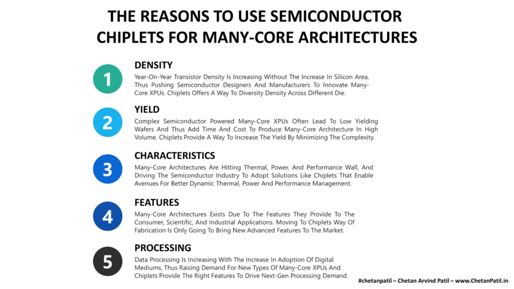
To cater to the need of future processors (built around Many-Core requirements), computer architects have come up with chiplets based designs and manufacturing methodologies. Chiplets provide a way to overcome design and manufacturing walls by diversifying complexity across multiple-die, thus provide more room for features.
Density: Transistor density has only increased without the increase in the silicon area. The reason is the demand of customers to pack more features without compromising on the die size. In reality, transistor shrinking will hit a wall, and that is when Moore’s law will end. For such future scenarios, chiplets provide a way out by spreading the transistors (for a given block) into multiple dies, thus allowing more room for future advanced features without compromising the area and cost aspect. Wrapping chiplets for Many-Core architectures also enable options to crunch data in shorted time possible and is the major reason why performance-oriented XPUs are focusing on chiplets.
Yield: Increasing complexity in a given area has a direct impact on the wafer yield. Low-yielding wafers are also not a piece of good news for the business. By diversifying the complexity into small set in different dies, chiplets provides a way to capture the yield and thus improve the production rate. High-yield is one of the benefits of chiplets and any other disaggregated method. Hence, chiplets are suited for Many-Core architecture.
Characteristics: Power, area, thermal, and performance aspects are a few of the technical characteristics that are critical in making a Many-Core architecture relevant for a specific application. Chiplets provide more area and thermal room and thus driving power and performance to a new level. It is something that Many-Core architectures aim for, and chiplets are a way to improve the power and performance by leveraging the area for better thermal management.
Features: Faster processing, multiple applications, handling complex data are some of the must-have features for Many-Core architectures. Chiplets are a perfect way to enhance features due to the IPs blocks residing on different dies, thus providing more room for management of resources.
Processing: Server grade processors geared towards scientific and research communities have only one goal: process the data as fast as possible. Doing so requires Many-Core architecture that can swiftly take the data in and present the results. Chiplets might (no evidence yet) interconnect and memory bottlenecks, something the majority of the Many-Core architectures suffer. Removing/reducing these two bottlenecks is also directly associated with faster processing.
Next-gen processor advancement is dependent on semiconductor technologies: Technology-node, devices, package-technology, etc. As the semiconductor industry enters the angstrom era (high on cost), there is a dire need to focus on semiconductor solutions (mainly for processor architectures) that provide a path towards a More-Than-Moore world.
While chiplets is one such design and manufacturing solution, it does has positive and negative consequences on the end-to-end semiconductor product development process.
THE IMPACT OF USING SEMICONDUCTOR CHIPLETS FOR MANY-CORE ARCHITECTURES
Chiplets provide a lot of flexibility to both the design and manufacturing aspects of the Many-Core architectures. However, all new semiconductor design/manufacturing processes also have an impact (positive and negative) on the overall end-to-end semiconductor product development process.
In the long run, disaggregated chips (chiplets) are supposed to overcome all the challenges faced by aggregated chips. There are several challenges that methodologies like chiplets solve (discussed in the last section), but chiplets adoption also comes up with new (and old) challenges.
What Is Chiplets: Chiplet is a singulated die (out of wafer) of a processing module. Several chiplet combined make up a larger integrated circuit (example: processor) called chiplets.
Many-core architecture built around chiplets will face both technical and business challenges. The only way around these is the continuous research and development activities so that next-gen chiplets overcome some of the following impacts semiconductor chiplets have.
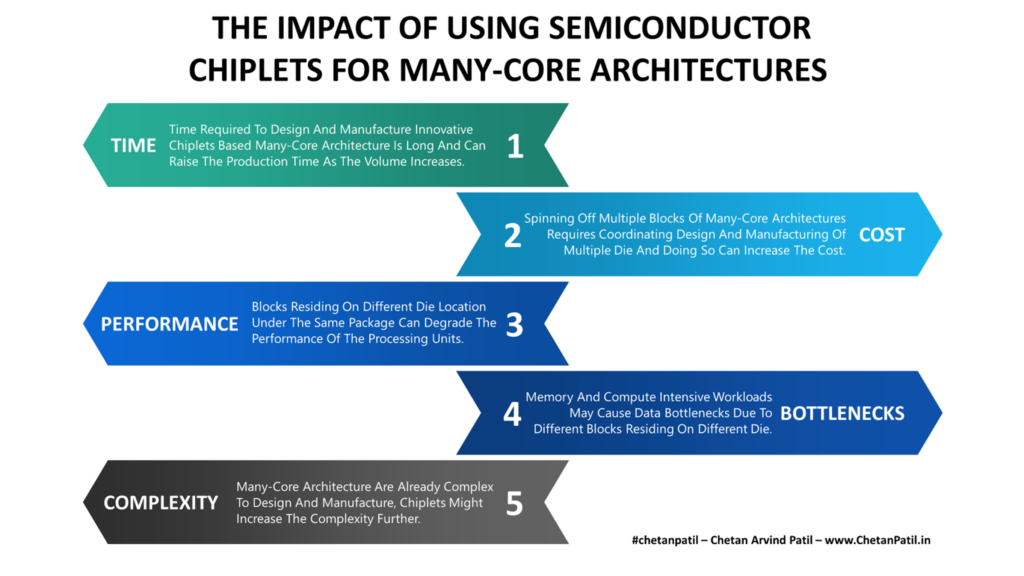
Time: One of the challenges chiplets face is the design and manufacturing time. The design team should ensure that each of the separate chiplet blocks will work as per the specification, more so when chiplet are combined to form chiplets. The same questions arise during the manufacturing time. In the end, both require design and manufacturing processes demand time, which can be an issue as the innovation pace and manufacturing volume increases, thus impact Many-Core chiplet based architecture.
Cost: On the semiconductor manufacturing side, chiplets can be costly (manufacturing) due to the different types of wafers required to bring the single chiplets to life. While the increasing cost can get balanced out due to the high yield, the semiconductor testing and assembling cost will still come into the picture. Even the package-technology required to glue different chiplet might increase the cost of manufacturing, and thus Many-Core architecture following the chiplets approach might end up costing more than today’s Many-Core solutions.
Performance: For a group of chiplet to work, a high-speed bus is required to ensure multiple chiplet can communicate together. While several such high-speed solutions do exist, it can also be the case that as the number of chiplet(processing blocks) increases per chiplets, the performance can degrade due to time added to coordinate tasks among different chiplet. Today, the only handful of chiplets based architecture exits, and applying it to Many-Core might bring performance questions.
Bottlenecks: Chiplets based Many-Core architecture can have lower performance due to the increasing bottleneck (memory and interconnects). The majority of today’s Many-Core architecture already suffer from it. If Many-Core chiplets architecture does not solve this problem, it means an existing problem found its way into the new system.
Complexity: Chiplets designing and manufacturing could bring a lot of complexity. From the design perspective: It will increase the number of simulations, rules (layout), analyses, and validation. From the manufacturing aspect: It simply demands a new supply chain approach. This is due to the fact that multiple wafers (each having one set of chiplet) will be required to ensure the right die from different wafers is glued together to form the end Many-Core system.
Chiplets are a welcome move and will push Many-Core semiconductor design and manufacturing processes. On top of all this, chiplets will drive new semiconductor testing and assembly methods for disaggregated chips.
Several XPU focused semiconductor companies have already shown elegant solutions around chiplets. These new developments are pushing other companies to adopt semiconductor chiplets. All this is only going to bring new types of Many-Core architectures.
In the long race, as the semiconductor industry moves towards the chiplets era, it needs to balance both the positive and negative impact to ensure the end-solution is as at part today’s solutions.
The semiconductor industry has been utilizing data to drive design and manufacturing for a very long time. The reason is the high cost and penalty of manufacturing a product without thoroughly reviewing the semiconductor data.
The growing importance of data is the primary reason why the semiconductor industry has always found ways to capture data cleanly. Capturing relevant data has helped semiconductor design and manufacturing. However, as the reliance on semiconductor data grows, it is crucial to implement end-to-end data integrity.
Semiconductor Data Integrity: How accurate, complete, and consistent semiconductor product-related data is.
Data integrity questions arise in the semiconductor (and several other industries) industry when for any given process steps or product, there are parts of the data that are missing or not traceable. Such miss-steps can occur when there is a need to go back and look at the historical data to capture any deviations that might in the future lead to re-calls (a process that the automotive industry has mastered and deployed for decades) to avoid failure in the field.
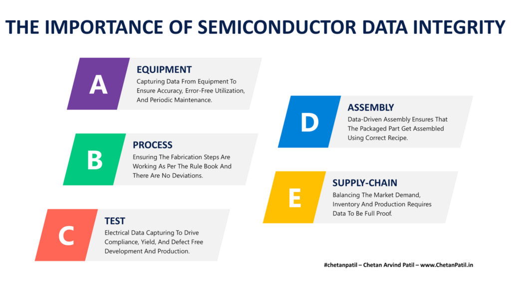
There are specific sub-steps in the semiconductor product development (mainly the manufacturing side) process that should be compliant from a data integrity point of view.
Equipment: Advanced equipment gets used for semiconductor testing, validation, and manufacturing. Capturing the data correctly and accurately is key to validating the product behavior. Any miss-steps causing data integrity issues can lead to an incorrect decision which can eventually cause losses in terms of revenue and time.
Process: There are thousands of steps that every semiconductor chip has to follow during the fabrication stage. Data is the only way to validate whether the process steps (lithography, etching, etc.) got successfully executed. If the data is missing or not correctly captured, then a faulty product will get fabricated.
Test: Electrical data during the post-silicon stage is required to validate the compliance aspect of the product development apart from capturing yield trends/issues. Data integrity during electrical testing is vital in driving accurate conclusions. An incorrect assumption or analysis (due to inaccurate data) can have negative consequences during the production phase.
Assembly: Assembly data integrity is vital as it is the final stage of any manufacturing process. After assembly, the parts get delivered to the customers. Any last-minute data points that can alert the manufacturing houses of possible issues can eventually save thousands of dollars apart from saving time. Hence, data needs to be accurate and compliant.
Supply-Chain:Balancing the inventory with market demand is a vital part of the semiconductor industry. Doing so requires relying on market intelligence. Thus the data provided by the market intelligence tools should be error-free. Hence, data integrity also applies to the data-driven supply chain.
Above are the handful of areas where the semiconductor data integrity is applicable by default. There are still specific steps that semiconductor companies/industry needs to revisit to ensure that product that goes out in the market has end-to-end data integrity.
In the long run, applying data integrity to semiconductor product development provides a positive impetus for the semiconductor industry/company. On top of that, it pushes them to produce more critical products for a wide range of industries apart from enabling customers with information about any data points that can have both negative and positive impacts on semiconductor products.
An efficient semiconductor product development process requires semiconductor data integrity and should be a default feature. Otherwise, the semiconductor data collected and analyzed can lead to incorrect decisions that can severely impact the new product launch.
Over the last decade, several new data solutions have taken the process of semiconductor device design and manufacturing to a whole new level. However, there are still opportunities to apply data integrity around specific steps. Doing so will raise the bar of the semiconductor company deploying data integrity features, as it will encompass an error-free process.
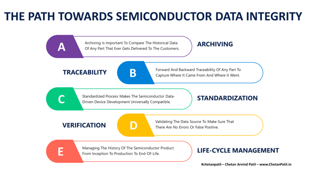
Archiving: Long-term storage of semiconductor data should be the first and foremost goal of any semiconductor company. Faster storage and retrieval drives efficient data analysis to capture different features of a given product. There is a need for default features to validate the archiving process to capture gaps or missing data points. Such features will ensure any data retrieved in the future will be reliable, completed, and accurate. Thus data integrity needs to be a default part of archiving process.
Traceability: Traceability allows connecting the data to a specific product. Billions of semiconductor products get shipped out every year, and it is critical to capture every actionable data a given semiconductor product generates. It demands a unique and robust traceability process so that the data can be correctly connected to the right product, thus driving next-gen data integrity in the semiconductor. Several approaches are already present, and as more products get shipped out, the importance of traceability will only grow.
Standardization: Semiconductor industry has several standards it follows diligently. However, it is important to keep revisiting these standards to ensure that the latest learnings from different semiconductor companies (and processes) are applied. It will drive further make the standardization processes more robust. The semiconductor industry should also focus on data standards by bringing more efficient data formats that are easy to store, parse, use, and analyze. All this can ensure end-to-end data integrity.
Verification: Data generation is half job done. It is also vital to verify the data generated. Cross-checking, validating properties, questioning data, and analyzing are keys to ensuring the semiconductor data is 100% compliant and is accurate. Moving forward, semiconductor companies relying on data analysis will have to by default deploy data verification techniques to capture any anomaly, thus avoiding miss-information and driving data integrity by default.
Product Life-Cycle Management:Product life-cycle management software tools have been around for decades. Cloud-driven solutions have also positively impacted product management, mainly the bill of material. However, slowly these software tools are becoming complex. Complexity makes the process error-prone and can lead to inaccurate information, thus affecting the data connected with the product. PLM tools will have to evolve and produce simple, minimal, and robust solutions that minimize human efforts and maximizes efficiency by keeping data integrity at the center stage.
The majority of the above points are already in place but are becoming complex due to the increasing semiconductor data (along with products) year on year. Managing data without losing its integrity should be the default focus of the semiconductor data solutions provider and users (semiconductor companies). Any missing points or issues at the source can invite confusion in the future. Hence, capturing and solving the gaps at the first step should be the goal of semiconductor data tools.
The semiconductor data integrity will also be a key for the emerging semiconductor FAB-LESs and FABs. It certainly requires investing in the new semiconductor data handling process. In the long run, it also implies that the demand for talents with data skills for the semiconductor industry will keep increasing.
The semiconductor industry consists of different players (companies) playing one of the two games: Finite Or Infinite. The technical and business planning laid out by any semiconductor company can enable classification of whether they are playing the long-term infinite game or sticking to a finite game.
The reason for this classification is a consolidation of semiconductor companies. It is applicable for both the design and the manufacturing side of the semiconductor. However, comparatively semiconductor manufacturing has seen more players that get classified as finite or infinite players. Primarily reason is the vast investment required to drive the next-gen semiconductor manufacturing, something not all companies can do regularly.
Finite Game: Played by semiconductor companies who have settled for a specific semiconductor technology that will be relevant for a very long time. It can also consistently drive revenue and market share.
Infinite Game: Played by semiconductor companies who are always looking to innovate and drive the industry forward by continuously developing future semiconductor technologies.
The ability of a semiconductor company to play an infinite or finite game is primarily driven by the resources and CapEx. Another factor is the arena or the domain the semiconductor company is catering to. For example, semiconductor design companies will have a different focus than semiconductor manufacturing (IDM or Pure-Play – whose business is driven by what semiconductor technologies they can offer).
Different criteria are used to clearly define the semiconductor companies into finite or infinite game players.
Focused Node: Finite semiconductor game players have long settled for specific technology nodes. They always focus on improving it without massive investments or resources, but the outcome always gives them the edge by making their current solution more efficient. The focused semiconductor technology process also means that finite semiconductor players do not actively expand their facilities/capacity.
Specific Market: The finite semiconductor game players also focus on one domain/market. They do it successfully by ensuring that all the different types of products (a market needs) are manufactured using homegrown semiconductor technologies. The specific market the finite semiconductor game players target is already matured but requires a finite semiconductor game player with years of experience in developing a specific technology (Example: mature nodes like 40nm or older).
Low-Cost: Though investment is part of the finite semiconductor player strategy, but in the long run, they do not heavily invest other than improving their existing facilities and design houses. It allows them to be nimble and ensures the focus on the specific node and market is enough to provide revenue to keep driving their business forward.
Rigid Process: In several cases, the semiconductor technologies developed/used by the finite semiconductor game players are firm and non-adaptive. There is a small room for improvement mainly because the solutions are already stable and mature. Changes occur but are not game-changers, and are simply different flavors of the same semiconductor solution. Example: Coming up with a different sub-process of CMOS 40nm but not improving it to reduce the node size.
Lacks Roadmap: Finite semiconductor game players focus on developing established processes without long-term planning. The main reason is the focus on the specific node without deviating from the existing (devices, interconnects, etc.) solutions. Finite semiconductor game players have a roadmap but is drastically different than the industry-level roadmaps that have primarily driven Moore’s law forward.
What has worked for the finite semiconductor game players is the focus on specific semiconductor technologies. Several semiconductor manufacturing companies (mainly focused on CMOS-driven higher/mature nodes) fall under the finite player category and have successfully survived in the semiconductor industry.
The finite semiconductor game strategy can also be a good path for new semiconductor manufacturing players setting up base in countries without prior semiconductor manufacturing infrastructure. Once the finite semiconductor game players have settled, then few of these players can follow the infinite semiconductor game strategy to develop the semiconductor manufacturing ecosystem. It can help countries like India that do not have private semiconductor manufacturing facilities.
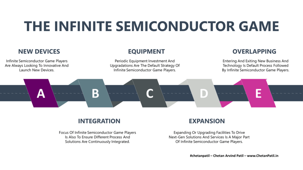
The finite semiconductor game players are focused on specific semiconductor technologies. There are infinite semiconductor game players who focus on today’s demand but on advancing different semiconductor technologies to ensure the future markets have new and improved semiconductor solutions.
Examples of target technologies by infinite semiconductor game players: Next FET devices, trying out new wafer size, opting for 3D stacking and vertical integration, and many more. All such (and many more) technological developments on the semiconductor front are critical. The infinite semiconductor game players are the primary reason why today the world is equipped with tiny smart devices capable of driving high-performance demanding solutions.
Like finite semiconductor game players, the infinite semiconductor game players also focus on specific technology development that caters to their market to drive revenue.
New Devices: The infinite semiconductor game players continuously develop new types of devices (FETs, etc.) to ensure they push the boundaries to launch new processes into the market. GAAFET, MBCFET, and RibbonFET are few such examples. These devices drive the semiconductor technology forwards and are the primary target of all the infinite semiconductor game players.
Integration: Apart from a new device, the infinite semiconductor game players also focus on integrating new approaches to enhance the existing semiconductor manufacturing strategy. For this, the semiconductor manufacturing companies, with infinite game strategy, focus on Front, Middle, and Back End-Of-Line innovation. These three stages ensure that the next-gen devices and processes are far more efficient (voltage, current, power, and performance) than today.
Equipment: In terms of upgrading semiconductor equipment regularly, infinite semiconductor game players are the leaders. It is the primary reason why the new semiconductor technology requires new equipment, and without it, an infinite semiconductor game player cannot survive.
Expansion: To drive a new type of semiconductor technology (packaging, testing, nodes, etc.), semiconductor companies with infinite game strategies need to keep expanding their facilities. It can be either by upgrading existing manufacturing houses or by opening new facilities in newer locations. Infinite expansion to capture the new market with new semiconductor technologies is the default strategy of the infinite semiconductor game players.
Overlapping: The infinite semiconductor game players also focus on extending their business by entering a new arena. It can be in the form of Intel providing the Foundry Services, or TSMC targeting the package innovation. All such big and bold moves are part of the infinite semiconductor game players and an important reason why they have survived for a long time and will keep pushing the semiconductor industry to new levels by keep playing the infinite game.
In the long run, the finite and infinite semiconductor game players are focused on their market. Each of these two sets of players is pushing their needs based on their internal strategy. Some players have the capital and resources to keep playing the infinite semiconductor game, while some are playing it safe and focused on the finite semiconductor game to drive their revenue.
As the world moves towards more advanced semiconductor technology with expanding semiconductor manufacturing capacity, there will also be the need for both finite and infinite semiconductor players.
THE MAJOR BLOCKS OF THE SEMICONDUCTOR FOUNDRY ROADMAP RACE
Semiconductor foundries across the globe are focused on providing solutions to retain existing customers and attract new customers. To achieve these two goals, semiconductor foundry companies have to keep innovating. Innovations are critical to ensure the solutions offered by foundries will spearhead the growth of new semiconductor products, thus the customers.
Semiconductor foundry roadmap plays a vital role in empowering customers with the future of semiconductor foundry technology. These roadmaps require years of research and development and are often in line with where the semiconductor industry is heading. Roadmaps also attract investors, and achieving roadmap milestones without delay is more important than ever. Any slip in achieving the milestones can directly impact customers and can derail market position.
The semiconductor foundries focus on several aspects of semiconductor technologies to drive semiconductor manufacturing forward. However, there are specific blocks that the majority of the semiconductor manufacturing players focus on as part of their long-term roadmap.
Technologies: Semiconductor foundries run on different types of semiconductor technologies. These semiconductor technologies are driven based on the product focus and capabilities of a given foundry. Semiconductor foundry fabricating only memory devices is more inclined towards (Example: Micron focuses on novel ways to increase layers of memory cells) providing memory-oriented semiconductor technologies. Similarly, analog, digital, or mixed-signal fabricating foundries focus on next-gen photo masking, etching, passivation, lithography, etc., to set their fabrication technology apart. The drive to focus on a specific technology (as per the foundry requirement) is the primary reason the yearly semiconductor roadmaps (from different companies) are focused on solutions that can enable future semiconductor technologies (devices, materials, etc.). Doing so can also expand the market share.
Devices: Devices are the basic building block of any silicon product. In the last few decades, the size of these devices (FETs) has only shrunk, thus providing more area to pack different types of processing blocks without utilizing a large silicon area. These devices have shrunk in size due to the massive research and development (between academia and industry) activities coupled with advancements in semiconductor equipment technology. Device research and development activities also need to be part of roadmaps to ensure next-gen solutions (like MBCFET, Next-Gen FinFET, etc.) cater to the requirements of both the foundries and the design houses.
End-Of-Line: Semiconductor fabrication requires three different lines/steps: Front, Middle, and Back. Front-End-Of-Line (FEOL) focuses on creating the structures that make the chip active as per the voltage and current requirements. Back-End-Of-Line (BEOL) process steps are primarily concerned with connecting different layers/blocks via complex interconnects. Lastly, to bridge the gap between the FEOL and BEOL, Middle-End-Of-Line (MEOL) is required. MEOL provides structures that serve as small contacts (like interconnects but have a specific and niche use/purpose during the fabrication) between different active regions of transistors. These three fabrication steps are the base of any silicon product. To keep up with Moore’s law, FEOL, MEOL, and BEOL have to be on the semiconductor foundry roadmaps so that every foundry can differentiate its process technologies from others and in the long term can provide unique solutions.
Materials: Similar to semiconductor devices, semiconductor materials also are one of the building blocks of semiconductor products. In reality, semiconductor products heavily utilize semiconductor materials during the manufacturing steps. The semiconductor foundry business will not exist without semiconductor materials like Silicon, Germanium, Gallium Arsenide, and several more. Apart from the basic periodic table materials, the semiconductor industry is also dependent on different kinds of chemicals. In the end, the semiconductor industry is built on top of basic science like any other industry is. Almost all semiconductor foundries focus on the materials aspect. However, given the slow change in new techniques around materials, the emphasis on semiconductor materials is not as big as any other aspect of semiconductor fabrication. Continuously improving the device efficiency means that the semiconductor foundries also need to focus on new types (Carbon nanotube, compound semiconductors, etc.) of materials to enable new solutions.
Automation: Semiconductor manufacturing (fabrication, assembly, and testing) is highly automated and requires minimal human interference to process the wafers. Semiconductor automation plays a vital role in ensuring that the lots get processed with the maximum throughput possible. Along the way, automation also captures/predicts issues that can empower semiconductor foundries with information to avoid delays and cost. The importance of automation has only grown in the semiconductor industry, and the dependency means automation technologies have become the default part of the semiconductor foundry roadmap.
Semiconductor foundries have focused on roadmaps for decades. It has helped them come up with next-gen technology and has also pushed the semiconductor technology race forward. Semiconductor Pure-Play Foundries and Integrated Device Manufacturers (IDM) are known for charting specific roadmaps that have always driven semiconductor manufacturing forward.
However, as the race to come up with the next-gen semiconductor manufacturing solutions grows, there is a need to focus on specific solutions that can push the manufacturing aspect of the semiconductor towards the angstrom era of devices.
THE NEW BLOCKS OF THE SEMICONDUCTOR FOUNDRY ROADMAP RACE
The continuous integration of new devices without increasing the silicon area has provided a new path for semiconductor design and manufacturing. Today, slim and compact electronics products are only possible due to the advent of a new class of semiconductor devices and technology-node that have ensured that the area required is not a hindrance to providing required power and performance.
Semiconductor researchers in collaboration with foundries have focused on several semiconductor technologies that have pushed the boundaries of semiconductor manufacturing so far. In the years to come, semiconductor foundries will need to focus on the new (examples below) building blocks of a roadmap for the semiconductor foundry.
FIN: The building blocks of semiconductor products are the devices. Until FinFET, these devices were planar. Starting with FinFET, the semiconductor design moved towards 2.5D. However, the need to scale further and put more transistors without compromising power and performance requires using 3D devices built using nanowire (GAAFET) and nanosheets (MBCFET). For increasing transistor density beyond Moore’s era, the semiconductor foundries will have to look into future devices that can utilize the FINs on the FET to drive the industry beyond 1nm and into the Angstrom era. It will require different foundries to focus heavily on a roadmap that purely focuses on developing new multi FIN-based FET devices.
xUV: Lithography is one of the critical fabrication process steps and also the costliest of all. Today, the most sophisticated UV technology to drive lithography is Extreme Ultraviolet (EUV). Only a handful of semiconductor foundries around the globe are capable of fabricating wafers using EUV equipment. The reason is the cost and also the fundamental issue like defects leading to reliability concerns. Technology like EUV is critical to meet semiconductor foundry’s technology-node goals. The semiconductor industry is on its way to surpass 2nm technology-node, which will require cost-effective and error-free lithography techniques that can enable devices transistors size of 1nm and beyond. It is only possible if semiconductor foundries work with semiconductor equipment manufacturers to drive a roadmap for next-gen lithography technology-powered equipment.
ABCD: Semiconductor foundries are fabricating hardware devices, but doing so requires several software solutions to keep the production line up and running apart from achieving the high yield, low defect, and faster throughput. All this is possible due to the focus on the ABCD (A = Artificial Intelligence, B = Big Data, C = Cloud, D = Digital Transformation) approach the semiconductor foundries have taken for a long time. As the world moves towards new semiconductor capacity, the need to drive next-gen ABCD solutions that are low on cost but high on efficiency will grow. Semiconductor foundries will have to keep innovating internally to ensure that the ABCD approach gets implemented via a roadmap to achieve the target (yield, scrapping, errors, etc.) results to drive minimal waste with maximum output.
Stacking: FinFETs tool the semiconductor industry from 2D devices to 2.5D devices. And today, the semiconductor industry is gearing to expand the FINs to enable the next-gen devices like CFET. CFET utilizes the folding approach to keep nFET on top of the pFET, thus securing the stacking approach for a real 3D integration. Stacking will also ensure that the next-gen devices utilize far less silicon area than today’s devices. It also requires innovation on the package-technology side, but the first step is always fabrication. Several device-level solutions exist that can transform horizontal integration into vertical. It will ensure the semiconductor industry keeps increasing the transistor density. However, there are still thermal, electrical, and failure (apart from cost) challenges that require a continuous improvement plan with the help of long term stacking roadmap.
Efficiency: Semiconductor products are defined based on how efficient they are. Efficiency does not mean low-power consumption but is about achieving the perfect balance of power, performance, and area (PPA) as per the target application. To achieve the balance of PPA, several semiconductor technological solutions from equipment, wafer size, devices, materials have to come together. Devices might be the most dominating aspect of achieving a balanced PPA. However, to fabricate these devices, different other semiconductor building blocks are required. Semiconductor foundries will have to have a roadmap that focuses on the power, performance, voltage, and area characteristics of the next-gen technology-node is at par with any given solution that exists today.
Several semiconductor manufacturing companies are gearing up to increase the worldwide installed semiconductor manufacturing capacity. However, increasing capacity is only half the job done. What is needed is the focus to keeps bringing new semiconductor manufacturing technologies that can excite the customer and drive the market towards a new era of semiconductor solutions.
The new upcoming semiconductor foundry capacity will require a semiconductor roadmap that drives new types of technology-node, equipment, automation, and other solutions. Semiconductor foundry’s roadmap from different competitors will ensure tomorrow’s semiconductor products are better than today’s and will also push the innovation around the products that semiconductor silicon devices are powering today and in the future.
The cost of semiconductor manufacturing is doubling every four years. The major driving factor for the rising cost is the product complexity due to the introduction of new technology-node and packaging technologies. Electrical testing also has played a role in increased manufacturing costs due to the demand for advanced automated equipment.
All such costs are directly associated with the increase in transistor density with shrinking die area. The increase in transistor density has also lead to several semiconductor manufacturing struggles. These struggles (have been around for decades) are an indispensable part of the semiconductor manufacturing process.
Advanced and automated equipment often helps solve the unknown and known struggles. However, the demand to increase the number of lots processed per hour adds a constant pressure to ensure that every wafer/die/product that gets processed is using an error-free recipe.
While the semiconductor manufacturing process has numerous steps, some steps do require special attention to capture any issues before it leads to shipment of bad products/parts.
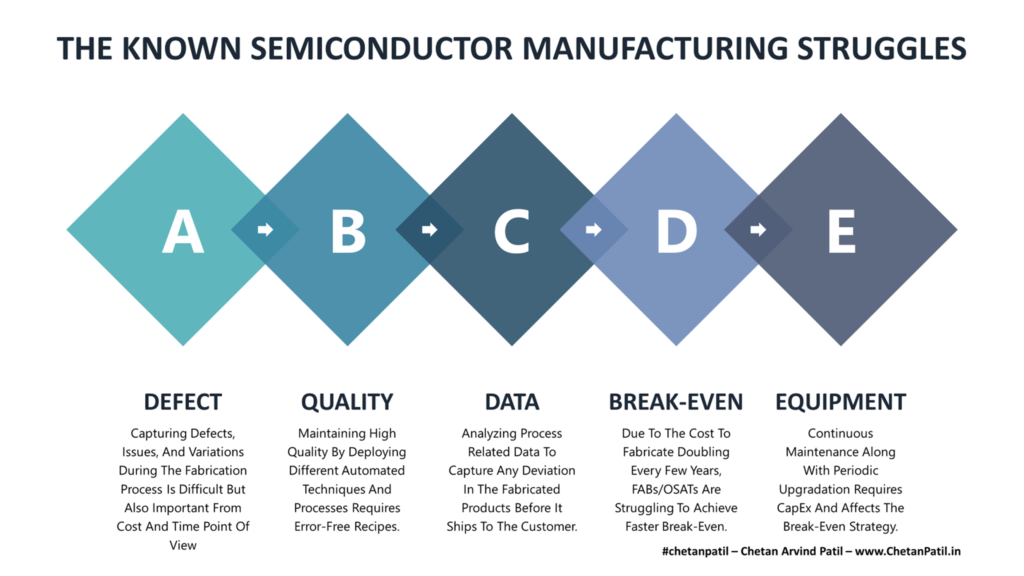
Defect: Fabricating, testing, and assembling thousands of dies often leads to defect. The defectivity rate is considerably low today than it was a few decades back. However, recipes are required to ensure that any wafer or assembled part is defect-free. Capturing defects is a manufacturing struggle, mainly due to the increasing layers/devices in the small silicon area. Sophisticated tools do capture defects, but a new type of defect can escape the fabrication scrutiny. Any such escape leads to known struggles of increase in processing time and cost.
Quality: Qualifying products is an important pillar of semiconductor product development. Depending on the product type, the qualification process has to follow standard steps before the product can be mass-produced. The industry standards do allow the easy flow of qualification. However, it is still a big struggle to ensure that all checks and processes get implemented correctly. As semiconductor products become more advanced, the cost and time associated with qualification (and failure analysis in case of part failure in the field) processes are rising. All this is pushing the qualification part of the semiconductor product development through the unknown to known struggles.
Data: Semiconductor and data go hand in hand. For decades, designers and manufacturers have spent a lot of time and effort to streamline a data-driven semiconductor product development process. However, as new advanced products get designed/manufactured, the cost of data capturing, analyzing, and storing is also rising. It is another struggle that the manufacturing process has to deal with. On the positive side, data today has become an integral part of semiconductor manufacturing, and so have been the tools to support data science activities to capture processes to defects. In the long run, the data struggle will keep increasing.
Break-Even: Cost of fabrication, testing, and assembly is rising. The capacity crunch is adding fuel to it. As new semiconductor technologies get launched, the cost of semiconductor manufacturing is rising. It also means that semiconductor manufacturers have to struggle their way through a long time before they can start earning net positive revenue. While this is true for several other manufacturing industries, the high CapEx that semiconductor manufacturing requires is very high and comes with risks.
Equipment:Every new semiconductor manufacturing technology (technology-node, package-technology, materials, chemicals, etc.) also pushes the need for a new type of equipment. It puts the FABs and OSATs through a continuous cycle of semiconductor manufacturing up-gradation, and also the equipment manufacturers, who have to struggle their way out to keep bringing new advanced equipment to drive next-gen semiconductor manufacturing technologies.
The above processes are just the handful of known struggles that any semiconductor product has to go through. Several sub-processes also exist and also require continuous monitoring to identify any known/unknown manufacturing issue.
Semiconductor manufacturing already has several recipes and equipment to ensure that the target number of lots is processed per hour, apart from ensuring that every wafer/part works as per the specification. However, to achieve such a goal also means to overcome several unknown issues that can show up during the semiconductor manufacturing process.
Apart from the known semiconductor manufacturing struggles, several unknown issues can pop up during semiconductor manufacturing (fabrication, testing, and assembly). These struggles are not like never seen before but remain classified as unknown due to the new information that is generated when such issues occur during the semiconductor manufacturing process.
Known Struggles: These struggles are part of the product by default, and a set process to capture issues around these processes already exists.
Unknown Struggles: These struggles are similar to known ones, but often through-off the product flow due to new issues that never existed before.
The time, cost, and efforts required to solve these unknown mysteries often impact the development cycle time. Any slip or late capturing of unknown issues can further increase the CapEx required to drive the product manufacturing and might put the semiconductor companies in tough spots.
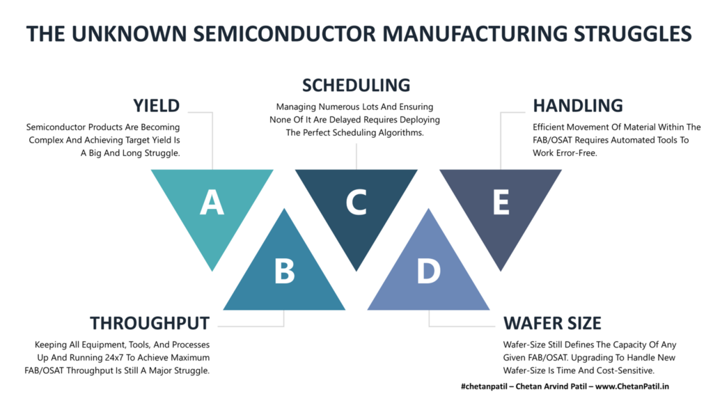
Yield: Yield can make or break a semiconductor product. The data captured at every manufacturing step has a direct or indirect impact on the total yield. Yield issues, if any, are often based on several factors. While the majority of the yield issues can be solved without extra time/cost, there are often unknown issues that take up a lot of time and effort. As semiconductor manufacturing becomes complex (new devices), there will be unknown yield issues that will keep bringing unknown struggles.
Throughput: Keeping high uptime is a challenge for FABs and OSATs. However, there are often issues that are not known and can lead to lower throughput, and thus increases the cycle time of semiconductor product development. Throughput struggles are due to equipment downtime, new process testing, high demand, capacity crunch, and several other factors. The last two years have already shown how such unknown (high demand) throughput struggles are affecting the semiconductor supply chain.
Scheduling: Managing thousands of orders is a big challenge of semiconductor manufacturing. Scheduling techniques are used to ensure all the products/wafers are processed in a timely manner. Any unknown spike in demand or issue with any of the processes brings unknown scheduling challenges for the FABs and OSATs, and they often have to re-prioritize activities to ensure the cycle time does not increase for their customers. This is another unknown struggle semiconductor manufacturing has to often deal with.
Wafer Size: Every FAB and OSAT is defined based on the wafer size/capacity. There is a point wherein FABs and OSATs realize that the current wafer size/capacity is not enough. It implies FABs and OSATs now have to invest in new facilities, which brings an unknown challenge of whether the semiconductor manufacturing capacity should be based on new wafer size or should only be an expansion of current facilities (with same wafer size). The answers to these simple questions severely impact the future roadmap of any semiconductor manufacturing company and thus brings unknown planning and investment questions/struggles.
Handling: Materials are constantly moving in the FAB and also in the OSAT. Often the automated system used to drive material handling and processing go down, and several impacts material handling/processing. Such downtime of material handling brings unknown scheduling to processing challenges. It also often happens that the manual handling of materials leads to wafers getting scrapped, and this is another unknown variable that can occur anytime during semiconductor manufacturing.
Like any manufacturing industry, the semiconductor industry/manufacturing has to go through different phases of known and unknown struggles. These struggles do impact the time or the cost aspect of semiconductor manufacturing and often both.
In the last four to five decades, semiconductor manufacturing has seen several advances (technology to processes to facilities) that have only helped ease the manufacturing of semiconductor products. As the world moves towards more semiconductor-driven products and solutions, the hope is that new next-gen semiconductor manufacturing solutions (tools, equipment, data-driven approach, etc.) will lower the known and unknown semiconductor manufacturing struggles.