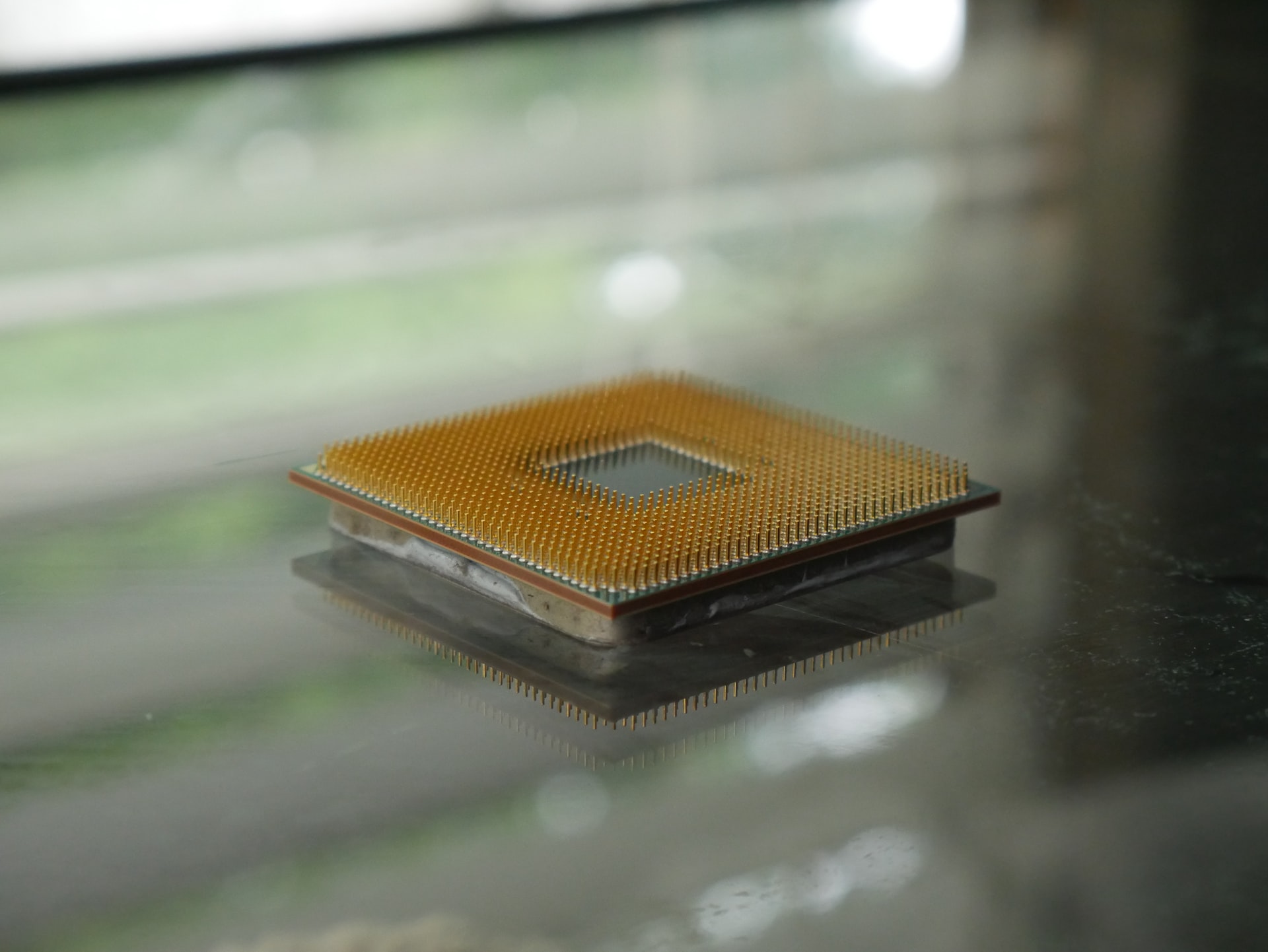
Photo by Matt Duncan on Unsplash
THE HURDLES FOR THE SHRINKING SEMICONDUCTOR ROADMAP
Several roadmaps get initiated by different semiconductor companies and also semiconductor technical bodies. These roadmaps provided a path of where semiconductor technologies were, where it is today and where it will be tomorrow. In many cases, roadmaps also allow a way to understand how the product development phase will be for any given domain within the semiconductor industry or company.
These roadmaps are based on the capabilities of any given company to drive semiconductor technological innovation. These innovations then eventually push the industry towards the next-gen of solutions that set the path for future research and development. For example, the mass production of 2nm is heavily dependent on EUV technology, and when such a solution is used at a large scale then enables the development of more die-to-device-level optimization and research.
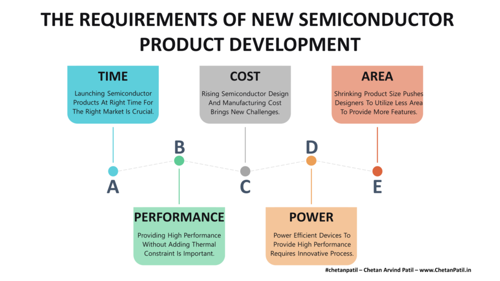
However, the continuous push to innovate and provide more balanced power and performance has now brought the semiconductor industry to a point where there are several challenges that companies (and the industry at large) need to overcome. These challenges will eventually enable new opportunities that will move the semiconductor product innovation ahead.
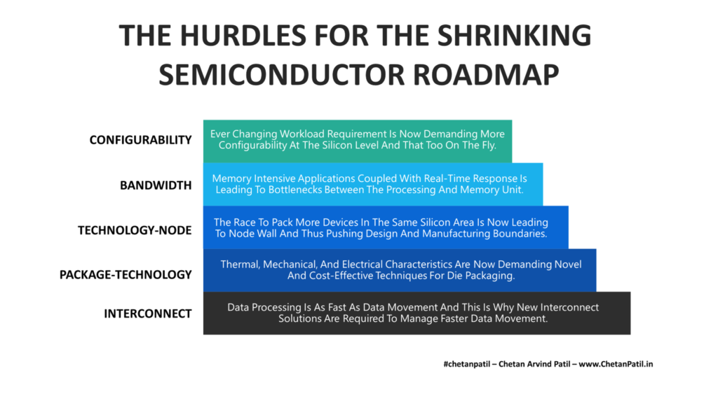
Configurability: The computing workloads in the 1990s were far less complex than the workloads today’s computing architectures are running today in the 2020s. For lighter workloads, a rigid IC (mainly XPUs) is perfect. Today, the workloads are changing due to the new data that gets generated faster than ever. That demands configurability from the lower level architecture to drive away any architectural bottlenecks. Configurability at the silicon level is all about adapting internal features based on the workload type. Configurability is hard to validate (apart from making it hack-proof), and the mass production of high-level configurable architecture remains a distant dream and a big challenge.
Bandwidth: Memory-intensive applications often require XPUs to read and write data to/from memory at a fast speed and that too at a high rate. Such continuous data movement is possible only if the memory bandwidth is large enough to drive faster data throughput. Theoretical maximum memory bandwidth overall has been increasing. It is mainly due to new XPUs that utilize memory interfaces via a high-bandwidth memory controller. There are applications (on the server-side) that require much larger bandwidth for faster GB/second to keep up with the read/write request from the processing unit. It is a challenge for semiconductor memory companies, as they gear up for the 5G+ and Edge computing world where every data point will have to get processed on the go.
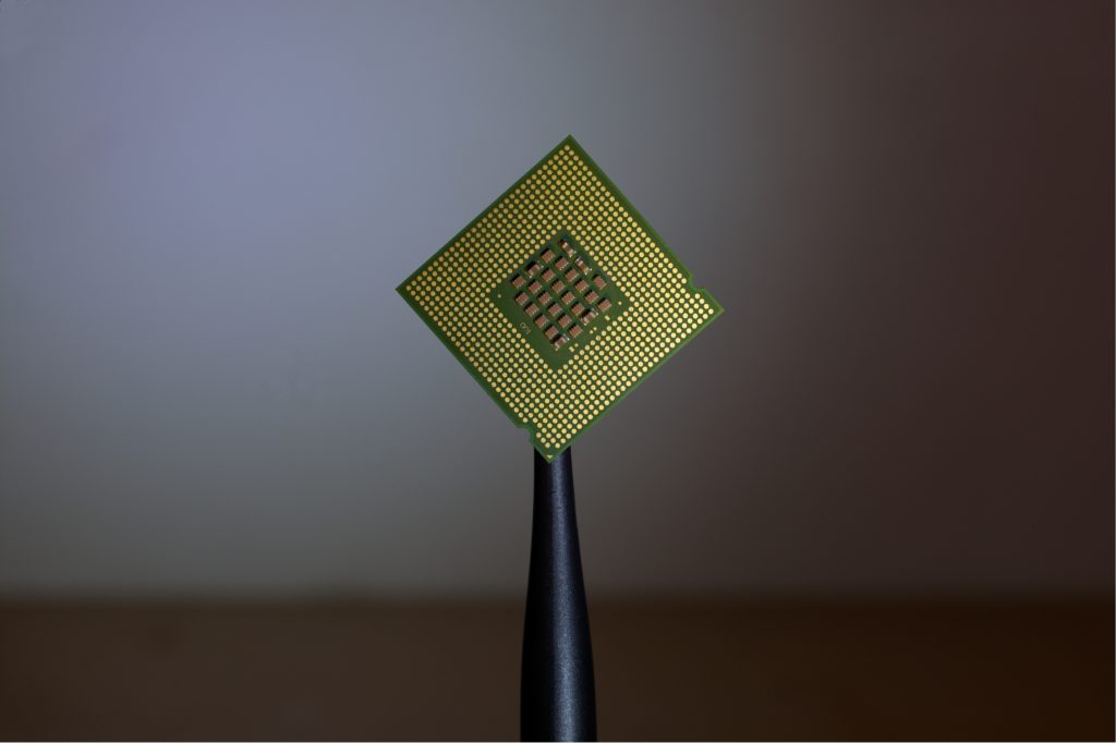
Technology-Node: Research-driven design and development have enabled the shrinking of transistors. Today billions of transistors get fabricated in silicon chips to provide the highest performance possible. However, the race to pack more devices is now leading to a device scaling bottleneck. On top of that, device scaling is also pushing the boundaries of science (physics, chemistry, and math). The semiconductor industry is still marching ahead and is ready to touch the 1nm technology-node and then move to the angstrom era. The design and manufacturing challenges brought with the new device scaling era will be endless. The semiconductor industry will have to move beyond just focusing on the shrinking of the technology-node.
Package-Technology: The shrinking transistor size is not only affecting semiconductor manufacturing but also has impacted package-technology. The semiconductor industry has already found solutions by utilizing 2.5D/3D techniques as an avenue to drive next-gen package-technology. There are still thermal, mechanical, and electrical challenges that are not easy to solve with every growing silicon density. Today, disintegrated packaging solutions are being used to integrated different components to balance the device characteristics.
Interconnect: Any given silicon product has different blocks interconnected via different network topologies. Interconnect allows data movement and transfer between multiple processing units. The speed of the processing units itself drives the application response time. As the number of processing units has increased in XPU, managing the data traffic is becoming a challenge. The electrical interconnect is also leading to higher power consumption as the data traffic is increasing. Thus putting the semiconductor solutions to adopt for alternate techniques to drive next-gen interconnect. Optimizing other alternate interconnect (photonics) solutions is going to be a big challenge for XPU designers.
The semiconductor industry has followed the roadmap approach for a very long time. Such a continuous outlook has pushed the boundaries of semiconductor design and manufacturing. The roadmap is also the reason why several innovative semiconductor-powered solutions are coming out in the market. There are certainly challenges due to Moore’s law scaling down. However, these challenges are creating new opportunities and driving the semiconductor industry towards the More-Than-Moore era.
THE OPPORTUNITIES FOR THE SHRINKING SEMICONDUCTOR ROADMAP
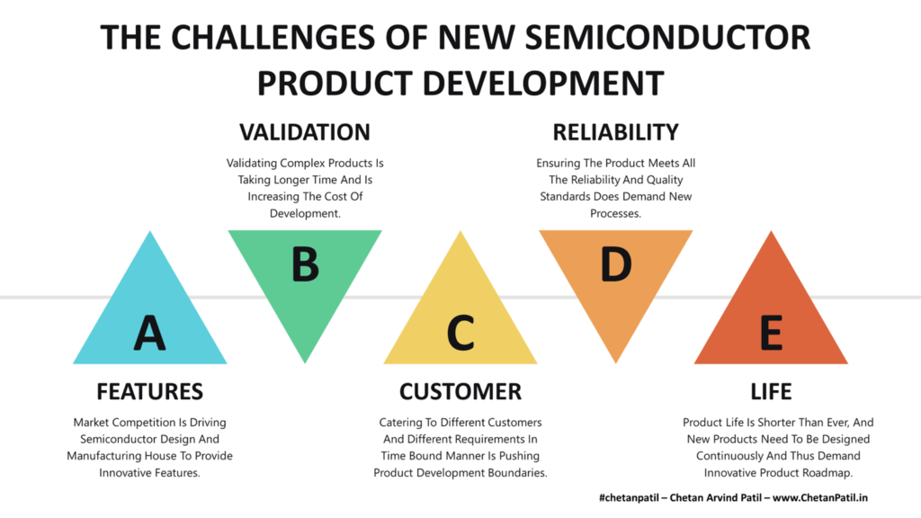
The shrinking semiconductor challenges are also an opportunity for the semiconductor industry. These opportunities push the envelope of the semiconductor industry and thus create the roadmap for future technologies.
The growing need to pack more transistors using different processes or methods has provided the semiconductor industry to drive new design ideas. Several semiconductor design innovations have matured from the research stage and are being used to manufacture next-gen devices. The drive to provide a new optimized approach is opening up the future roadmap for the semiconductor industry.
These roadmaps are build by the opportunities created by the challenges that the industry faces today.
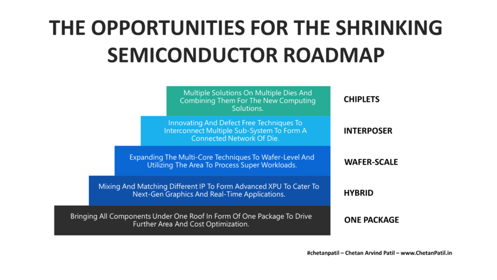
Chiplets: Increase in transistor density without increasing the silicon area leads to bottlenecks. These bottlenecks are not only around design (power and performance) but also on the manufacturing side. The manufacturing technologies (via technology-node and equipment support) have advanced to enable device fabrication at 2nm. The thermal, mechanical, and electrical characteristics (due to the small silicon area) are posing a challenge to the XPU design. Such challenges are also presenting a new opportunity for XPU designers. Semiconductor XPU design companies have now adopted the multi-die technique to spread the silicon area, which also has the potential to improve overall yield. AMD and Intel have already demonstrated XPUs with chiplets for multi-die XPUs, and will certainly dominate the market (in terms of design/innovation).
Interposer: Chiplets manufacturing required the use of multiple dies. Connecting these different blocks to form an integrated chip/system often requires a specific silicon technology called interposer. Semiconductor companies often use different interposer terminology, but eventually, the underlying goal of each of these is to provide a common place for two or more die/blocks. Interposers usage will grow with the growth in chiplets adoptions. It also means providing optimized network-based topology to arrange/stack different blocks for efficiency, which is an opportunity for the research and development teams across academia and industry.
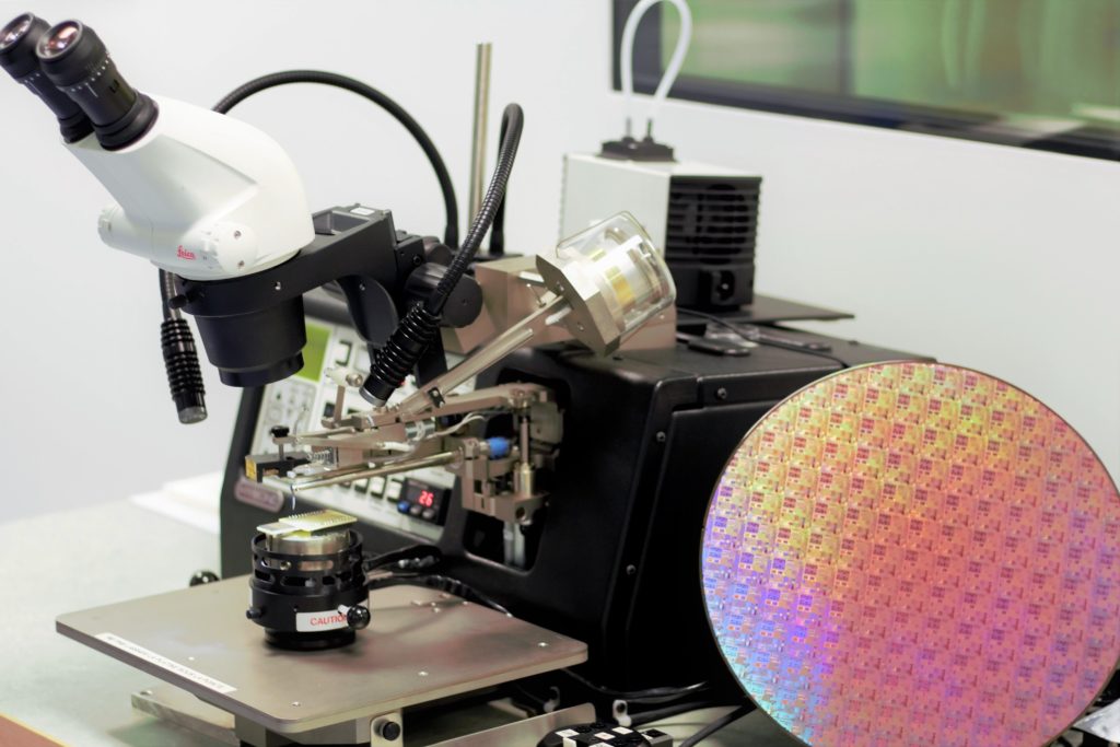
Wafer-Scale: Servers to supercomputers are getting faster every year. The need to shrink the data centers while not compromising on the throughput is pushing semiconductor design and manufacturing towards large-scale wafer-level solutions. For such solutions, the wafer-scale integration approach comes in as an opportunity to provide die areas as large as the wafer to create high-performance processing units. These units can then cater to any data demand of today and the future. Due to the advancement in semiconductor manufacturing, the yield at the wafer level will not be an issue, but the cost aspect can be.
Hybrid: Monolithic chips have been in use for several decades. Later, monolithic chips got replaced by multi-core homogeneous and heterogeneous architectures. As the world moves towards a more remote-enabled world, the need for multiple hybrid architectures will grow. These hybrid architectures will have unique processing characteristics, which will enable semiconductor design and manufacturing companies to leverage new methodologies like chiplets to heterogeneous architectures to mixing/matching IPs, thus providing an opportunity to expand the semiconductor roadmap.
One Package: System-In-A-Package (SiP) allows a way to integrate multiple systems under the same package technology (carrier package). Given the proliferation of multi-die integration, SiP will take the central stage. One package approach will allow semiconductor companies to provide a unified packaging approach to stick together different dies/IPs under the same substrate. While this will pose a challenge, the past success around similar package technology will smoothen this approach.
Continuous technology development is the key to ensuring that the semiconductor roadmap keeps moving forward. These new technological solutions also enable different industries that leverage the new design to manufacturing methodology to drive better customer experience.
As the semiconductor roadmap inches towards the 1nm era, it will be vital to keep innovating to move the world into the angstrom arena.