Photo by Carlos Irineu da Costa on Unsplash
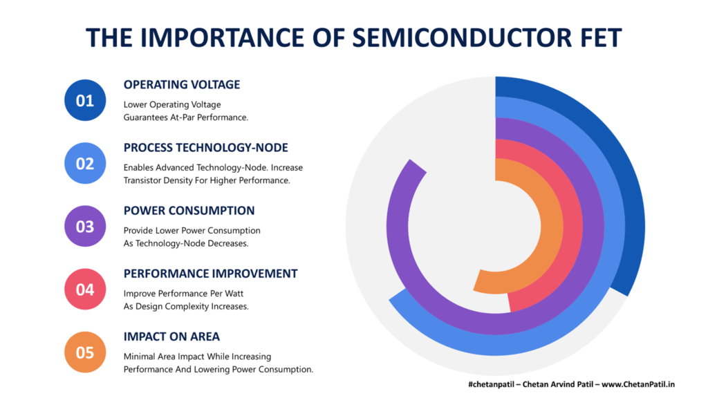
THE IMPORTANCE OF SEMICONDUCTOR FET
Cells are the building blocks of life. Similarly, transistors are the building blocks of the semiconductor industry. In the computing world, transistors lay the foundation for any type of processing solution.
Transistor performs the basic function of toggling between HIGH (ONE/TRUE) and LOW (ZERO/FALSE) state. Such basic function when performed by zillions of transistors together, drives several technological solutions from car safety to wireless data/voice transmission.
The need to make compact computer-powered solutions has pushed the development around the transistors over the last four decades. These development have been both on the design and the manufacturing side.
Transistors used in semiconductors are often called FET – Field-Effect Transistors. The function performed by FETs is the same as traditional transistor. The only aspect that has changed over the years is the form factor which changed in order to follow the Moore’s law.
The main goal of FET is to improve Power-Performance-Per-Area (PPA). To do so, following technical aspect has to be fulfilled before the FET design can be used to manufacture next-gen hardware:
Operating Voltage: A perfect FET will be the one that can perform as per the specifications. As the technology-node shrinks, the operating voltage also goes lower due to the advancement in the FET design. The major reason is to accommodate the dynamic and static power consumption along with the leakage. Lowering voltage has negative impact to, but that is compensated with the unique designs of next-gen FET.
Process Technology-Node: Technology-Node shrinks faster than the development of new devices. Till then the devices go through a different non-planar to planar transformations to accommodate for the shrinking size. However, after a given point it becomes design and manufacturing-wise difficult to transform (like FinFET can only be stretched to a certain extent with the help of its fins) the same device type. After that, the material and drastic design changes are expected.
Power Consumption: FETs are present in a large number in any advanced technology-node systems like microprocessors. If FETs are not providing the lower dynamic power consumption (along with negligible leakage), then the purpose to use new designs is not fulfilled. Hence, device designers face an uphill challenge to ensure the increased density of the FET in a specific silicon area only leads to lower power consumption, not higher.
Performance Improvement: Apart from lower power consumption, performance improvement is another criterion that leads to new FET designs. Balancing power consumption along with performance is difficult. However, without these criteria, there is no way to ensure the next technology-node will have a better impact and use case than the previous one.
Impact On Area: Eventually, the goal of shrinking technology-node is to ensure the area of the silicon chip does not increase for the same or more computing tasks. This means the design of new FETs will have to be more 3D than 2D/2.5D. Otherwise, in the long run, it becomes a bottleneck for the designers to make use of the FET without impacting the silicon area.
The FET is the building block of modern semiconductor solutions and there are already several types of FET that are available and used based on the technology-node.
Both academia and the industry have contributed equally in bringing new FET design to the market, which today is powering almost all of the electronic products around the globe.
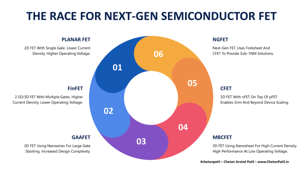
THE RACE FOR NEXT-GEN SEMICONDUCTOR FET
Given the race to be the first one to launch the next technology-node, the semiconductor companies (mainly semiconductor manufacturers) are also racing to come up with a new FET design that can cater to their needs while having minimal to zero impact on Power-Performance-Per-Area (PPA). During this course, the semiconductor industry has already seen many transformations in FET designs. From 2D to 3D.
Below are few active and future FET designs that the semiconductor manufacturer is pursuing:
Planar FET: These are the traditional FET that follow the 2D design. The source, the drain is on top of the substrate and is not wrapped around the gate. The power consumption and area impact is high. Planar FET mostly use nanowires.
FinFET: FinFET is an advanced version of planar FET. The source and drain are extended as fins and the gate wraps around them to provide a faster current flow. One drawback of FinFET is that the design might lead to manufacturing residuals around the fins. This can impact the quality of silicon chip being manufactured. However, FABs have found ways to ensure there are enough inspection steps to avoid such defects. FinFET is what today the majority of the manufacturing companies use to manufacture silicon requiring advanced technology-node.
GAAFET: FinFET has its advantage, however, to provide lower operating voltage and higher performance, the industry has also come up with GAAFET. GAAFET is geared to be used towards 3nm mass production along with FinFET. The difference between GAAFET and FinFET is the slicing of fins by making of nanosheets to drive much faster current flow that FinFET. This also allows greater switching control. This structure helps in shirking the size without impact the performance.
MBCFET: MBCFET has been developed by Samsung as part of their 2nm and beyond technology-node roadmap. Both FinFET and GAAFET use fins that are stacked vertically, thus not allowing the use of the area above the source and drain. To overcome this, MBCFET is developed that uses the same fins based nanosheets but are stacked horizontally to provide more area for current flow. MBCFET can also be designed using existing process tools and has the same area footprint as FinFET and GAAFET.
CFET: While the industry moved towards fin-based structure and started using nanosheets to provide more area within the same size, researchers have also been focusing on CFET which they are touting to be the next-big thing in FET design. The CFET is an advanced version of fin-based FET (even more advanced than MBCFET) and it uses the folding approach to keep nFET on top of the pFET. This can be done either via fins or sheets. It is like a high-rise structure with FETs stacked on top of each other. CFET still uses a nanosheet approach.
NGFET: These do not exist today. NGFET – Next-Gen FET – will be what the semiconductor industry will use when going beyond 1nm. It will borrow all the learnings from the prior generation, however, instead of nanosheet, NGFET will use forksheets. The forksheets will take a nanosheet approach by combining the vertical and horizontal fins to provide more density and performance.
While there are several FET solutions to choose from, the industry and the academia do understand the difficulties the semiconductor design and manufacturing bring when advanced technology-node process is used. Thus, leading to several new (and known) hurdles and challenges.
THE HURDLES FOR FUTURE SEMICONDUCTOR FET
Given the small area for improvement, new FETs are incredibly complex to design. While both the academia and the industry is focused on improving the FET design that lowers the operating voltage while balancing other technical specifications, there are certainly numerous hurdles to overcome.
Voltage: The smaller/advanced the technology-node, the lower the operating voltage. The primary reason is the ability to generate heat or damaging the devices (= FETs) when operated at a higher voltage. With every new generation/type of FET, the operating voltage is low. This also impacts the sub-sequent systems the advanced technology-node systems (using lower operating voltage FETs) are connected to. This means a new system is required to drive the data further at higher voltages. As FETs evolve beyond 3nm technology-node, such design constraint is something the device designers will have to consider so that the operating voltage is not too low for the silicon system down the line.
Leakage: Lowering technology-node means new device structures and it also means more transistors per given area. Operating all these devices at higher voltage can subsequently lead to leakage either through continuous operation or via thermal. Lowering the leakage is another challenge for FET device designers.
Thermal: Thermal is a tricky one to solve. The junction temperature is already high enough that it demands designers to embed temperature sensors to capture thermal effects. This certainly adds complexity to the design and also impacts the operating scenarios, which hinders from exploiting the full potential of the systems due to continuous throttling.
Performance: Lowering operating voltage as the FET evolves means also balancing the performance and area ratio. FET in the future will have tackle this three-way balancing act (voltage, performance, area) as the industry marches towards the 2nm and lower technology-node.
There are certainly several hurdles (apart from those listed above) for FET design and manufacturing. The semiconductor design and manufacturing industry will overcome these and many. Academia is also coming up with interesting FET solutions that can pave way for more elegant lower technology-node solutions without compromising on the voltage to performance to silicon area.
In the end, the FET design will keep changing and evolving in order to keep pushing the semiconductor industry forward towards More-Than-Moore world.