Photo by david latorre romero on Unsplash
THE NEED FOR AI SEMICONDUCTOR CHIPS
Multi-Core Processor (MCP) or Chip Multi-Processor (CMP) revolutionized the computing industry. MCP/CMP came up with advanced execution and parallelism techniques. Software took the opportunity provided by the multiple processors fused into the single System-On-A-Chip (SoC).
MCP also provided the advantage of Out-of-Order Execution (OoOE), instructions-level parallelism (ILP), thread-level parallelism (TLP), and interleaved Simultaneous Multithreading (SMT), and allowed multiple applications to run on the same processor or multiple cores in the same SoC. Soon, the Single Instruction Stream, Single Data Stream (SISD) evolved into Multiple Instruction Streams, Multiple Data Streams (MIMD). MIMD gave a new experience to the data-intensive applications in the post-internet era.
The semiconductor and computing industry took advantage of MCP for over a decade by incorporating different core/processing units into a single SoC. Multi-Processor/Core System-On-A-Chip (MPSoC/MCSoC) became the heart of the new data and memory-intensive application. MPSoC/MCSoC starting to come up with dedicated processing blocks for data related to the graphic (GPU), digital (DSP), vector/vision (VPU), neural (NPU), and High-Bandwidth Memory (HBM).
The Artificial Intelligence System-On-A-Chip (AISoC) Is The Need Of The Future AI-Driven Workloads And Applications
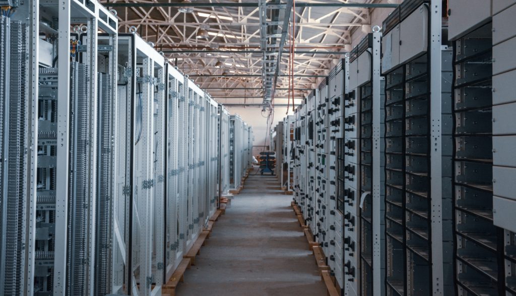
The software computing industry is demanding data be processed faster than ever from semiconductor chips. Shrinking the transistor size further is not allowing the data and memory-intensive AI/ML/DL workloads to make the best of the MPSoC/MCSoC. Even though there are many opportunities to improve and innovate by proposing smarter data management techniques (cache, memory, and threading), MPSoC/MCSoC seems to have hit the memory wall, area wall, power wall, thermal wall, and performance wall. The data centers that should be shrinking in size and space due to the technology node advancement are instead becoming large by churning out massively distributed systems with a large number of MPSoC/MCSoC connected with large memory (NUMA).
The data-intensive, compute-intensive and memory-intensive artificial intelligence applications/workloads demand SoC that is:
- Low Cost:
- Affordable to manufacture
- Efficient:
- Improved performance-per-watt (PPW)
- High Parallelism:
- Massively parallel execution without stalling
- Smart:
- Ability to generate/store/predict models on the go that reside closer to the cores
- Zero Bottlenecks:
- Processes the data without memory/interconnect bottlenecks with or without a co-processor
- Adaptive Software:
- Ability to get programmed with minimal high-level programming effort and adapts on the go
- High-Speed Memory:
- Provides a large amount of high bandwidth memory across different memory levels/hierarchies
- Technology Node:
- Works efficiently irrespective of the advanced technology nodes used
The above eight-point feature is what will pay the way for Artificial Intelligence System-On-A-Chip (AISoC). These AISoC will be critical for the next generation of advanced solutions that will find use in the growing autonomous world. AISoC can be used in all devices and not only in the data centers. AISoC can speed up the fast-changing automotive to the satellite industry.
To cater to the growing demand for the semiconductor SoC chips for Artificial Intelligence) and to also balance the complexity, cost, and time to market, the semiconductor industry has already started to move away from general-purpose cores to specialized cores.
While the semiconductor industry is not labeling these new SoC as AISoC, but the features offered are of the AISoC world. Not all the AISoC solution adhere strictly to the eight-point features discussed above, but the solutions offered by different semiconductor companies is a step in the right direction.

THE STATUS OF AI SEMICONDUCTOR CHIPS RACE
Leadership in AI semiconductor chips is vital. Countries across the world are competing to bring the best homegrown solution to establish the lead. Governments are also funding the semiconductor chip business with the hope of leading the semiconductor race and mainly the AI solution one.
Apart from governments, companies across the globe are also racing against each other. From software giants to hardware leaders, all companies are investing zillions of time and money to come up with AI semiconductor chips out in the market.
The Artificial Intelligence System-On-A-Chip (AISoC) development is happening in two parallel worlds:
- Established companies building in-house AI semiconductor chips
- Startups providing a new architectural solution to drive AI semiconductor chips market
Below is the snapshot of the world’s top established companies racing against time to bring AISoC not only for their consumption but also for the market:
Alibaba: Alibaba competes directly with e-commerce giants and mainly Amazon. It provides web services similar to Amazon Web Services. To cater to enterprise needs, Alibaba last year launched Hanguang 800 is capable of processing 78,563 images per second. Alibaba introduced XuanTie 910 in 2019 provides 40% more performance than reference ISA RISC-V. These two AISoC are only a handful of examples. Alibaba’s DAMO Academy is continuously innovating and is going to launch much more surprising products in the AISoC domain.
Alphabet/Google: Alphabet’s Google arm has always been into hardware research and development. Google’s Brain and Hardware and Architecture team has been continuously providing solutions to make AI algorithms faster and smarter. Several AI-related hardware solutions have come out of Google. Google Cloud’s TPU is already becoming a benchmark for the AI industry. There are already many solutions that promise to improve the time to train networks using large data sets. Google is also pushing the envelope by taking the help of AI to design AI chips. With Pixel’s line of products, there is more room to innovate. In the coming years, Google will showcase innovative AISoC solutions.
Amazon: Amazon caters to more than 200 million visitors per month. Every visitor provides Amazon business and also the data on his/her shopping behavior. To process and make use of such unique data and to also provide enterprises the efficient web services, Amazon has been investing in AI-driven chips for a long time. Amazon’s Inferentia is the first step towards conquering the server market that is AISoC powered. The growing Alexa line of products pushed Amazon to in-house AISoC development and the results are already been seen in form of smarter voice-assisted devices.
AMD: AMD is another established semiconductor company with AISoC products. With AMD Instinct and AMD EPYC line of products, AMD has been steadily growing its market share in AI-enabled devices. AMD is also making most of the semiconductor chiplets technology to bring more innovation at the silicon level. Its acquisition of Xilinx is only going to help bring more AISoC solutions to the market. AMD is not deep into the mobile space, but they can certainly take advantage of the growing gaming industry to compensate. AMD CDNA is also another breakthrough architecture design to speed up high-performance computing.
Apple: With the launch of M1, Apple has shown the world its next target is going to be more in-house Macbook and iPhone/iPad processors. M1 has a NPU that allows faster predictive actions for its users. Apple is also planning to launch X-Reality products, which will require elegant AISoC, for which Apple has already started the work.
ARM: ARM IP has been critical for the smartphone industry and has taken the lead in providing AI-powered chips for mobile and also the data centers. With TOP500 won by ARM-powered supercomputers, ARM is ready to come up with more AISoC solution. Smart homes, wearables, and smartphones will see a massive use of AI Chip that will be powered by ARM. With Apple going all-in for ARM processors, and it will also help ARM innovate on the AISoC front.
Baidu: Baidu is a giant in China and competes worldwide with Google, Amazon, and Alibaba. Baidu showcased the Kunlun AI processor during HotChips 2020 that is designed and produced in collaboration with Samsung Electronics. Kunlun is capable of catering to diverse AI workloads and claims to have three times more performance than NVIDIA AISoCs. It will be interesting to see how Baidu goes all in-house with AISoC designs.
Facebook: There are 2.7 billion people that used Facebook every month. To serve the growing requests, Facebook has been developing in-house silicon that takes advantage of AI to provide faster training. Zion, Kings Canyon, and Mount Shasta are three major AISoC that Facebook has innovated to run its hardware infrastructure efficiently. It has ramped up its effort to develop more in-house AISoC, and the results will be out in the coming years.
Huawei/HiSilicon: A subsidiary of Huawei, HiSilicion has been innovating fast to cater not only to the AI smartphone and data center market in China but also in the majority of the developing nations. The Kirin and Ascend line of products has done wonders for Huawei devices. Huawei has also launched AISoC for data centers. It will be vital to see how Huawei and HiSilicon innovate in the next few years and expand their AISoC portfolio.
IBM: IBM has been a quiet leader in smart technologies. Watson has done wonders for the AI industry and also pushed other companies to innovate faster. IBM has innovated to accelerate DNN training with the help of CMOS and new AI Cores. IBM has been focusing on Analog and Digital AI cores that enable dynamic and hybrid cloud systems. IBM is one of the few companies that not only provide AISoC based solutions but also innovates at the transistor level. The combination of two allows it to provide more efficient AI solutions than others.
Imagination Technologies: Imagination Technologies has also ramped up its AI chip efforts. Recently, it launched a new AI-powered BXT series of chips for data centers. PowerVR backed line of products have helped Imagination Technologies establish its foot in the vision processing domain. PowerVR solution combined with Neural Network Accelerators (NNA) is unleashing new ways to process vision data and will also enable new AISoC.
Intel Corporation: Intel is a leader in the server and data center SoC market. Even though it is getting stiff competition from other vendors, Intel has been able to provide the industry with breakthrough AI chips. Even though the Nirvana series of AI chips did not work out as planned, it has big planes with Habana’s line of products. The manufacturing capability of Intel allows it to ensure that there is always a new way to design and manufacture AISoC. Intel Xeon’s line of products has also shown how the AI world how smaller SoCs are capable of running workloads on high bandwidth memory. With shrinking transistor size and Intel’s plan to move beyond 7nm, there will be elegant AISoC coming out.
Infineon Technologies: Infineon Technologies is going big in the AI Chip domain. It has established an AI development center in Singapore and also has a series of MCU designed with AI in mind. Low-cost MCU running with AI capability is the perfect solution for portable smart devices like cameras, drones, and smart speakers. AISoC with inbuilt MCU is another avenue Infineon is capable of exploring.
Marvell Technology Group: Marvell has launched a series of ASIC-based accelerators to cater to the AI data demand. The custom ASIC solutions used high speed interconnects and innovative packaging to optimize performance and cost. On top, Marvell has a strong collaboration with TSMC to provide 5/7/14 nm AI ASIC that allows it to pitch a wide range of portfolio to the growing AISoC market.
MediaTek: MediaTek’s Helio line of AI chips for edge computing on the go. It is also planning to use the solution for the 5G market. Apart from the hardware products, MediTek also provides hardware-oriented design solutions like NeuroPilot to make the most of its AISoC with AI Processing Unit (APU).
Microsoft: Microsoft hardware division has provided many AISoC solutions to the market. Project Brainway is another such solution that allows the use of FPGA and ASIC to speed up the training. Microsoft also has plans to develop a tiny AI chip in collaboration with Sony. It may very well pave a new way for nanoelectronics well beyond what is available now.
NVIDIA: GPUs have single-handedly accelerated the growth of AI research. NVIDIA has been one of the leaders that showcased how to train the data set faster using GPU architecture. Apart from catering to the data centers, NVIDIA also provides AI-enabled SoCs for smart cars. A few months back, NVIDIA also unveiled cost-efficient A100 architecture for the industry. With ARM’s acquisition, NVIDIA is on track to bring AI to the low power AISoC soon.
NXP Semiconductors: NXP has several MCUs and MPUs optimized for AI applications and targeted for the automotive and smart industry. NXP’s i.MX series provides ML and DL optimized solutions. With growing semiconductor cost in automotive, NXP is stand to get the advantage with is a wide range of AI-enabled AISoC chip solutions.
Qualcomm: As mobile AI is growing, Qualcomm is taking advantage of it by providing On-Device AI accelerators. Qualcomm has also taken steps towards a cloud AI Chip solution. It launched Cloud AI 100 chips to showcase its new architecture design for AI and data centers. Stronghold on mobile business with already out AI chips, Qualcomm can spring a surprise and enable new data centers that are not only AI-enabled but are also low-power and efficient AISoC.
Samsung: Samsung has fingers in many pies. From the design of chips in-house to the capability of manufacturing chips for its products and the world. Like Qualcomm, Samsung has been pushing for an AI chip to enabled On-Device AI. It has also collaborated with Baidu to develop a server-class of AISoC. The advantage of owning a foundry allows Samsung to innovate end-to-end and will be vital to see if it goes in the data centers’ AISoC chip design and development.
Tesla: Tesla already has the smartest AI-enabled cars out in the market. It has already designed in-house an AI chip to cater to Tesla’s growing need to provide more advanced and safe autonomous car driving solutions. Rumours says that Tesla would do away with cars and focus on an AISoC solution that can make any vehicle an autonomous one. Whether or not it will end up happening, Tesla’s AISoC will push the innovation around the self-driving car.
Texas Instruments: Like NXP and Infineon, TI is also providing Edge AI chips that cater to the 5G market. TI’s manufacturing capability fueled with low power techniques is going to provide a way forward to the industry on how to innovate AISoC with low power consumption.
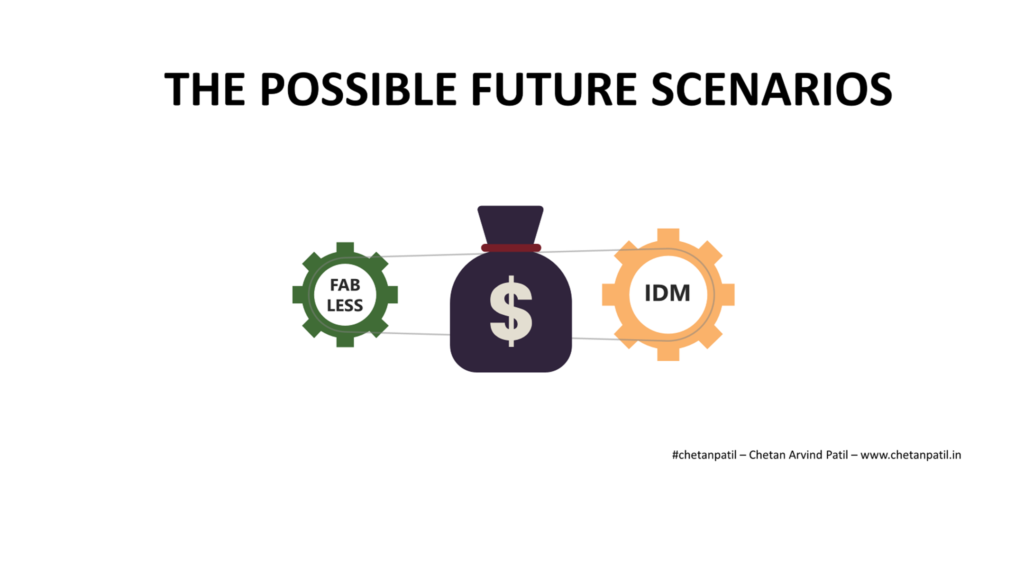
The above summary shows how established companies are innovating and launching AISoC. The cost to establish a FAB-LESS semiconductor startup has gone down. The advanced EDA tools provide the ability to test ideas in the shortest possible time. RISC-V open ISA is also helping innovate without investing in royalty based ISA.
All this has lead to an increase in the number of FAB-LESS semiconductor startups that are coming up with new semiconductor chip designs and solutions to cater to the AISoC market. These startups have already got traction and some are even collaborating with established companies to test the solutions.
Below is the list of some of the top startups coming up with silicon level technology to drive AISoC design:
AlphaICs: AlphaICs is focusing on Edge AI and has designed an AI Processor that finds application as both the mobile and the data center solution. AlphaICs call their AISoC as Real AI Processor (RAP)
Alphawave: Alphawave provides Digital Signal Processor (DSP) solutions that are suited for high-speed performance and are low on power consumption. DSP provides audio/video processing and with Alphawave’s AppolloCORE IP semiconductor companies can build AISoC with an onboard accelerator. Alphawave was also the winner of TSMC’s Awards for Excellence in Accelerating Silicon Innovation
Blaize: Blaize is another startup providing Edge AI solution that is built for AI workload. Blaize’s Graph Streaming Processor (GSP) is a power-efficient and adaptable core that caters to AI, ML and DL need on the fly.
Cambricon Technologies: Cambricon used to provide processors to Huawei before it began its own in-house silicon design house HiSilicon. Since then, Cambricon has developed several general markets AI products catering to mobile and cloud. Their Cloud AI platform provides flexibility and adaptability. With more than 100 million smartphones and servers powered by Cambricon, it is going to be vital for the AISoC world.
Cerebras Systems: Cerebras uses Wafer-Scale Engine technology to deliver a supersonic deep learning experience. It is benchmarked to be 1000 times faster than a GPU. Cerebras unique interconnects, memory, and package technology is pitched to break many records in computing shortly.
EdgeQ: EdgeQ is taking a different approach to Edge and 5G by fusing both into a single AI-powered chip. This will massively off-load the tas from data centers to Edge Computing. With 5G rollout already in progress worldwide, the solution is at the right time for the right market.
GrAI Matter Labs: GrAI Matter is targeting robotics, X-Reality, and the drone market by providing Edge AI Processor. The solution provided by GeAI Matter has ultra-low latency and is low power, two features critical for Edge processing.
Graphcore: Graphcore has accelerator products that cater to machine learning and artificial intelligence by leverage the proprietory Intelligence Processing Unit (IPU) technology.
Groq: Groq leverages Tensor Streaming Processor (TPU) to provide small programming cores that are packed in a tiny package with high-speed memory and performance fast operations.
Hailo: Hailo is one more startup focusing on Edge AI. Hailo claims its Hailo-8 Edge AI processor can provide 26 tera-operations per second (TOPS) without comprising the area and power efficiency.
Horizon Robotics: Journey and Sunrise processor architecture from Horizon Robotics is designed to provide an AI-enabled Brain Processing Unit (BPU). Journey BPU is designed for the automotive industry, while Sunrise is for the IoT market.
Kneron: Kneron provides Edge AI solution and plans to take on Google and others with its AI-enabled chip. Kneron claims its KL720 AI SoC has the highest performance to power ratio in the market.
Lightelligence: Lightelligence is taking a photonics approach to solving AI processing problems. It has already released an optical AI accelerator but yet to see mass production for the market needs.
Lightmatter: In the same domain as Lightelligence, Lightmatter also plans to use electronics, photonics, and algorithms to provide processor and interconnect that is faster and more efficient than traditional AISoC.
Luminous Computing: Still in stealth mode, Luminous also plans to leverage photonics to speed up A workload training.
Mythic AI: Mythic uses Intelligence Processing Units (IPUs) to provide power-efficient, performance-oriented, and cost-efficient AISoC. Mythic Analog Matrix Processor is already available to order and will find use in Edge AI.
NUVIA: NUVIA is a stealth mode startup focusing on ARM-powered CPUs to drive AI workload. More details about its architecture are yet to be known.
SambaNova Systems: SamaNova is another startup that uses Reconfigurable Dataflow Unit (RDU) to enable new models without going into the algorithm complexity. SambaNova’s Cardinal SN10 is designed to eliminate constant data caching and excess data movement, something the majority of the SoC today suffers from.
SiMa.ai: SiMa wants to make greener low-power AISoC for Edge AI. It is yet to share product details. SiMa plans to launch new silicon early next year.
SimpleMachines: To accelerate AI/ML/DL application performance, SimpleMachines leverages Composable Computing. Simple Machines AISoC solution enables flexible and powerful real-time computation.
Synthara AG: Synthara leverages RISC-V ISA to provide ultra-low power ASIC for Edge AI.
Syntiant: Syntiant provides an ultra-low power AI processing solution for any battery-powered device, from earbuds to laptops. Syntiant Neural Decision Processors™ (NDP10x) is a tiny silicon that is always-on.
Tenstorrent: Tenstorent Grayskull AISoC fast AI interference to enable accurate and faster prediction on the go. It is expected to into production soon.
Wave Computing: Wave wants to accelerate AI computing with the help of MIPS architecture. The M-Class product from Wave Computing provides AISoC using MIPS architecture for IoT and smart devices.
Both established companies and startups are showcasing the world’s new way to design chips and drive data processing. All this is making software development, training, testing, and data analytics faster. The AISoC from all these vendors is also providing avenues for low-cost AI-powered mobile and data centers.
However, there are several challenges ahead.
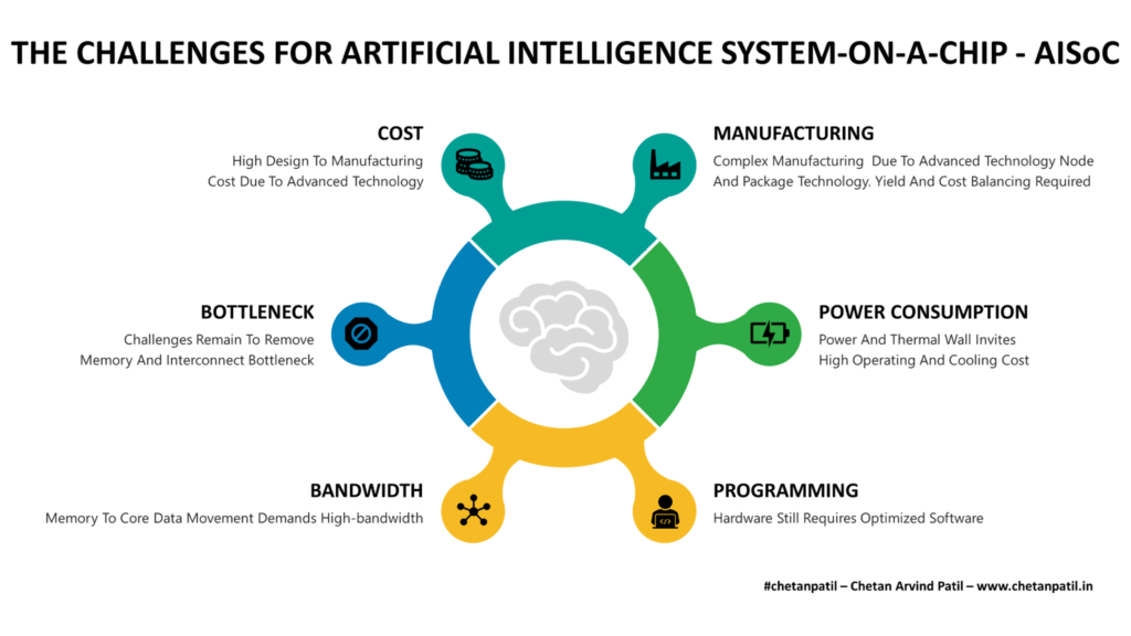
THE CHALLENGES AHEAD FOR AI SEMICONDUCTOR CHIPS
The majority of the challenges the AISoC face are still the same old problems faced by general-purpose CPU and GPU as the technology at the silicon level advanced. The new AISoC solution from both the established companies and startups are eventually going to hit with these challenges.
Cost: Designing and establishing AISoC proof-of-concept using the software simulator demands resource and pushes the cost of development from FAB to OSAT. The cost of owning smartphones and running data centers is already high. On top of it, any new solution with AI-power will add cost to the customer. The technology node required to enable a high number of processing units to speed up the training and inference is eventually going to cost money. AISoC vendors need to balance the cost of manufacturing in order to breakeven the market. On top of all this, the amount of competition in developing new AISoC means time to market is vital than ever.
Bottleneck: The reason to move away from general-purpose CPU and GPU was memory and interconnect bottleneck. There are few startups listed above that are trying to remove these bottlenecks. However, with the speed with which new AI-workload are getting generated, there is a high chance that bottlenecks will still exist. It will be vital to ensure that the new type of AISoC that both the established companies and startups are envisioning does not have any bottlenecks.
Bandwidth: Bringing the data closer to the processing units (any type) is the key to processing AI data faster. However, for such a task high-speed memory with large bandwidth is required. The new AISoC are incorporating new processing units like RAP, GSP, TSP, BPU, AMP, RDU, NDP, and so on, but there is no clear strategy and details on how the data communication bandwidth is improved. May be such details are proprietary.
Programming: In the end, any AISoC cannot process the data efficiently if the workload is not optimized for the target architecture. While few AISoC is pitching their products as no need to change the data or framework before running it on their architecture, however, the reality is that every architecture ends up needing some or other form of optimization. All this adds to the time to develop data solutions.
Manufacturing: As the new AISoCs come out in the market, many of these will end up using advanced nodes beyond 7nm to provide high speed. Advanced packaging technology also is required to operate the AISoC within the thermal budget. Both the complex technology node and package technology will drive a high manufacturing cost. Apart from this, balancing yield and cost will be essential to ensure AISoC development is viable.
Power Consumption: AISoC requires zillions of transistors that require faster cooling. The majority of the AISoC can do with liquid cooling but when such AISoC is connected together to form data centers then the cost to run data centers goes high. Hopefully, greener technologies will be able to run such data centers. However, the AISoC will get challenged to overcome the area, power, and thermal wall.
No matter what, AISoC in coming years is going to be the semiconductor domain that will innovate and provide elegant semiconductor solutions that will challenge the end-to-end semiconductor design and manufacturing.