Image Generated Using 4o
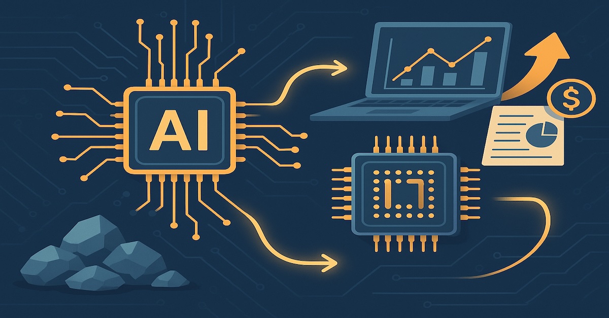
Why AI Matters In The Semiconductor Industry
Earlier this week, I had the opportunity to deliver a session at Manipal University Jaipur as part of their Professional Development Program on AI-Driven VLSI Design and Optimization. The event brought together students, researchers, and professionals eager to explore how Artificial Intelligence is reshaping the semiconductor landscape.
During this talk, we dove deep into the real-world applications of AI in semiconductor design, verification, and manufacturing. We discussed why AI is not just a buzzword but an increasingly essential tool to tackle the industry’s enormous complexity and relentless pace of innovation.
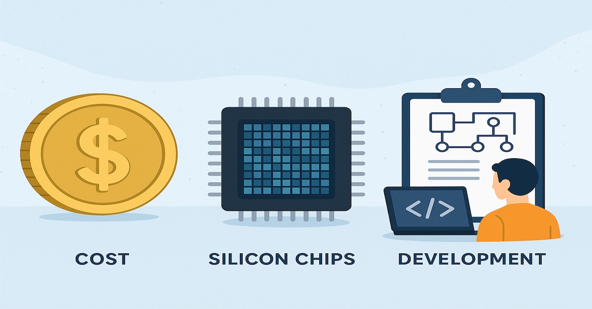
We all know that semiconductors are the invisible workhorses of our digital world. Every smartphone you use, car you drive, or cloud service you rely on depends on tiny silicon chips built with extraordinary precision. Yet designing and manufacturing those chips has become one of the most challenging engineering tasks of our time.
Traditionally, semiconductor development involves painstaking manual work and countless iterations. Engineers grapple with vast datasets, strict design rules, and manufacturing tolerances measured in nanometers. A single error can mean millions of dollars in wasted wafers, delays, or product recalls.
This is where AI comes in, not to replace engineers but to empower them.
AI offers transformative advantages for the semiconductor industry, such as:
- Accelerating Design Cycles: Automating tasks like layout, simulation, and code generation
- Improving Yields: Detecting subtle defect patterns and predicting manufacturing outcomes
- Enhancing Efficiency: Fine-tuning fab operations and preventing costly equipment failures
- Reducing Costs: Minimizing errors, rework, and scrap, which all contribute to faster time-to-market
However, AI is not a silver bullet. It still requires high-quality data, domain expertise, and human oversight to deliver meaningful results. Each challenge in semiconductor design or manufacturing often demands custom AI approaches rather than generic solutions.
Ultimately, AI matters because it helps engineers navigate the staggering complexity of modern chip development, enabling faster innovation and higher-quality products.

Two Big Perspectives: AI In Versus AI For Semiconductors
When we talk about AI and semiconductors, there are two equally important perspectives:
- AI in Semiconductors: How AI is used as a tool inside the semiconductor industry
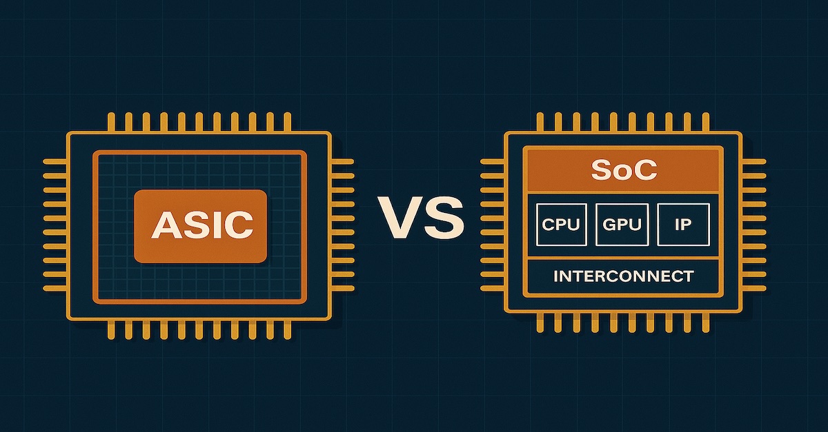
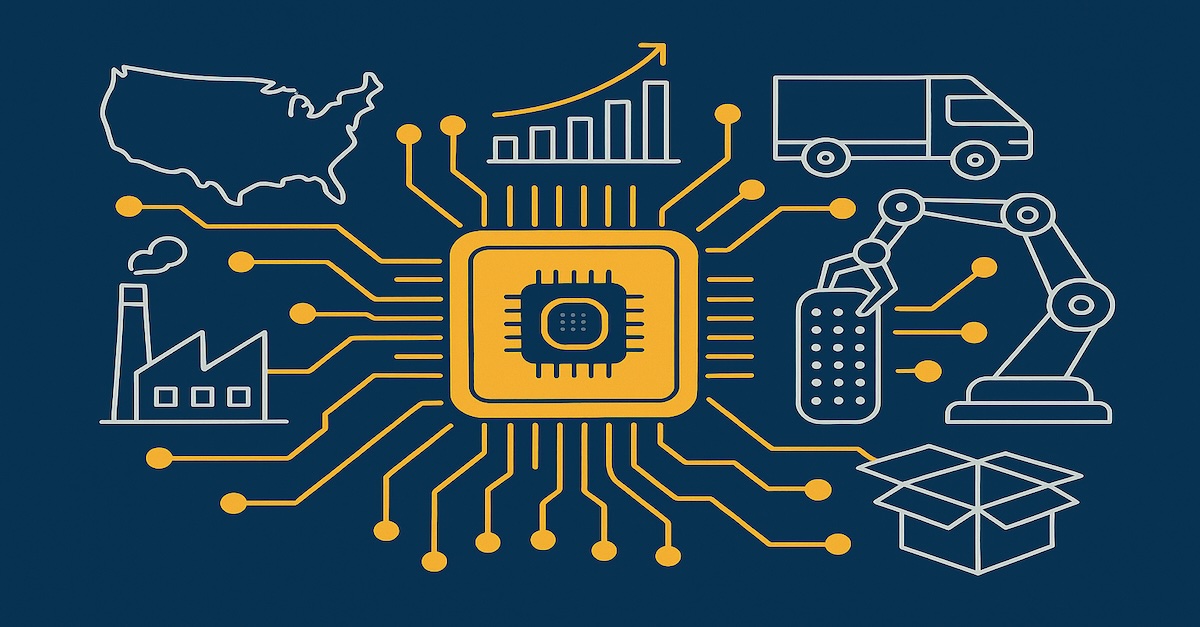
- AI for Semiconductors: How semiconductors are explicitly built to power AI applications
The table below summarizes the differences:
| Aspect | AI In Semiconductors | AI For Semiconductors |
|---|---|---|
| Main Role | AI helps improve how chips are designed, manufactured, and tested | Chips are designed specifically to run AI workloads faster and more efficiently |
| Key Benefits | – Faster design cycles – Improved yields – Predictive maintenance – Cost reduction | – High-speed AI processing – Energy efficiency for AI tasks – Enables new AI-driven applications |
| Typical Use Cases | – AI-driven EDA tools – Defect detection – Test data analytics – Fab process optimization | – GPUs and TPUs – Custom AI accelerators (ASICs) – AI-specific memory (HBM) – Chiplets for AI performance |
| Industry Focus | Improving internal semiconductor workflows and efficiency | Creating products for AI markets such as cloud, edge computing, automotive, etc. |
| Impact on Industry | Speeds up semiconductor development and manufacturing | Powers the broader AI revolution in multiple industries |

These two perspectives are deeply connected. For example:
- AI tools help design AI accelerators faster and more efficiently
- AI hardware built by semiconductor firms enables the massive computations needed for AI software used in semiconductor manufacturing
In essence, AI is improving how we build chips, and better chips are enabling ever more powerful AI. It is a cycle that is driving both technological progress and new business opportunities across the industry.
Practical AI Use Cases Across The Semiconductor Lifecycle
AI is not just a futuristic concept. It is already hard at work in real, practical ways throughout the semiconductor industry. From how engineers design and verify chips to how fabs manufacture silicon wafers and analyze test results, AI is becoming deeply woven into the fabric of semiconductor workflows.
Unlike traditional methods that often rely on manual effort and painstaking trial-and-error, AI brings speed, predictive power, and the ability to uncover hidden patterns in massive datasets. This makes it an invaluable partner for tackling challenges like complex design rules, defect detection, process optimization, and yield improvement.
Whether it is accelerating chip design with natural-language tools, optimizing manufacturing parameters in real-time, or spotting subtle defects invisible to human eyes, AI is helping semiconductor companies work smarter and faster. Let us explore how these applications play out across the semiconductor lifecycle, from initial design all the way to manufacturing and testing.
Here is a snapshot of where AI is making its mark:
| Lifecycle Stage | AI Use Cases | Benefits |
|---|---|---|
| Design | – Natural language to HDL code (e.g. ChipGPT) – Design-space exploration- PPA optimization | Faster design cycles, reduced manual coding |
| Verification | – Auto-generation of testbenches (e.g. LLM4DV) – Functional coverage analysis | Shorter verification times, higher confidence in chip functionality |
| Layout | – AI-assisted layout tools (e.g. ChatEDA) – Placement and routing suggestions | Accelerates physical design, reduces errors |
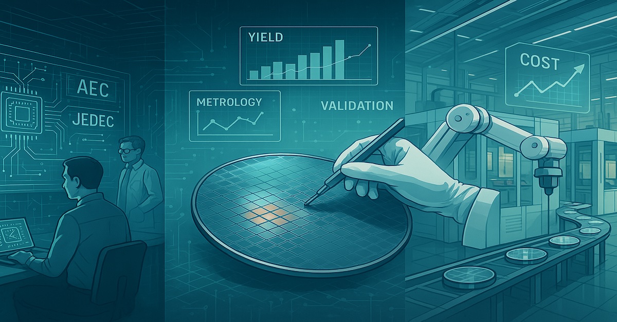
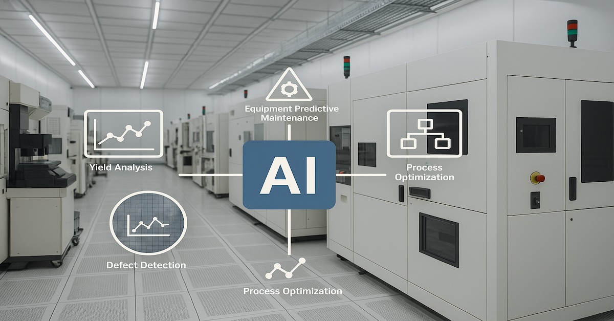
| Manufacturing (FAB) | – Computational lithography (e.g. cuLitho) – Process parameter optimization- Predictive maintenance | Higher yield, fewer defects, lower manufacturing costs |
| Testing & Yield | – Test data analytics – Defect pattern detection – Root-cause analysis | Improved test coverage, faster debug, yield enhancement |
Across the lifecycle, AI is stepping in to tackle some of the industry’s most complex challenges. In design, tools like ChipGPT are translating natural-language specifications directly into Verilog code, helping engineers move from ideas to functional designs with remarkable speed. In verification, AI models can auto-generate testbenches and assertions, reducing the manual burden and ensuring higher functional coverage, traditionally one of the biggest bottlenecks in chip development.

Manufacturing has seen dramatic gains from AI-driven computational lithography. For example, platforms like cuLitho use GPUs to accelerate complex optical proximity correction (OPC) calculations, essential for creating accurate masks at advanced nodes like 5nm or 3nm. Meanwhile, in testing and yield analysis, machine learning is analyzing huge volumes of test data, detecting defect patterns, and predicting yield outcomes, allowing fabs to tweak processes proactively and avoid costly rework.

Overall, these advances are not only saving time and costs but are also enabling engineers to push the boundaries of innovation. AI has become more than a tool, it is an integral partner that helps the semiconductor industry keep pace with rising complexity and shrinking timelines.
Building AI Skills For Semiconductor Professionals
As AI becomes increasingly embedded in semiconductor workflows, professionals across the industry need to level up their skills. The good news? You do not have to become a data scientist to thrive in this new era. But understanding how AI fits into the semiconductor ecosystem and how to work alongside it, is quickly becoming essential.
Semiconductor engineers, designers, and technologists should focus on practical, applied knowledge rather than deep AI theory. Here is what matters most:

Ultimately, building AI skills is not about replacing your core semiconductor expertise. It is about augmenting it. AI tools can handle repetitive analysis, crunch massive datasets, and suggest optimizations that would take humans days or weeks to discover. But it is still engineers who guide the work, validate results, and make critical decisions.
In this evolving landscape, those who understand both semiconductors and AI will be uniquely positioned to drive innovation, solve complex challenges, and shape the future of the industry.
The Road Ahead: AI As A Partner, Not A Replacement
As the semiconductor industry pushes forward, it is clear that AI will play an essential role. But despite the hype, AI is not here to replace engineers, and it is here to work alongside them.
From generating chip designs based on natural-language prompts to predicting manufacturing issues before they happen, AI is becoming an intelligent assistant that makes complex tasks faster and more precise.
Yet, AI is not magic. It still needs clean, high-quality data and human expertise to interpret results and make decisions. There is no single AI solution that fits every challenge in semiconductors. Engineers remain critical for guiding AI tools, validating outputs, and handling situations where nuance and domain knowledge are essential.
Looking ahead, the most successful professionals will be those who learn to collaborate with AI, using it to tackle complexity and unlock new opportunities. In the semiconductor industry, AI will not replace human ingenuity, it will amplify it, driving faster innovation and helping us solve problems once thought impossible.