Image Generated Using DALL-E
Importance Of Semiconductor Node Selection
Choosing the right technology node is among the most critical engineering and business decisions in semiconductor design, especially for ASIC (Application-Specific Integrated Circuit) and SoC (System-on-Chip) development. The selection impacts performance, power efficiency, area, cost, design complexity, and market viability.
As semiconductor technology advances, nodes have shrunk from 180nm in the early 2000s to cutting-edge 3nm and beyond, enabling greater transistor density, higher speeds, and lower power consumption.
However, transitioning to an advanced node is not always the best choice, designers and businesses must carefully evaluate multiple trade-offs based on technical feasibility, business impact, and long-term manufacturability.
Understanding Technology Nodes
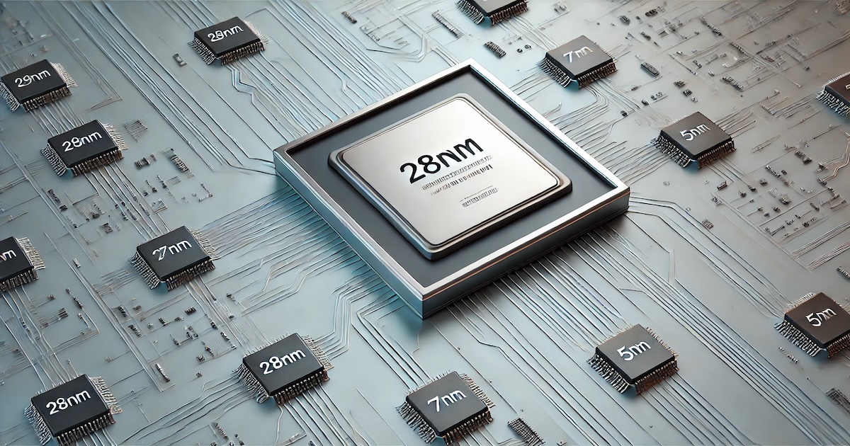
A technology node, often denoted in nanometers (e.g., 28nm, 7nm, 5nm), represents a semiconductor manufacturing process. Traditionally, this figure referred to the transistor gate length. Still, modern node names now encompass multiple process optimizations beyond feature size, including metal pitch scaling, contact efficiency, and new transistor architectures.
Key technology transitions:
- 180nm to 65nm: Introduction of copper interconnects, replacing aluminum for better performance
- 45nm to 28nm: The introduction of high-k metal gate (HKMG) technology reduces leakage and improves power efficiency
- 16nm/14nm: Transition from planar transistors to FinFETs, drastically improving performance and power
- 7nm and below: Extreme Ultraviolet Lithography (EUV) becomes necessary to print more minor features
- 3nm and beyond: Adoption of GAAFET (Gate-All-Around FETs) and stacked nanosheet transistors, enabling further scaling
Each transition increases manufacturing complexity and cost, requiring companies to strategically evaluate whether a given node justifies its investment. Thus making the semiconductor node selection for product development a key step.
Key Factors In Selecting A Semiconductor Node
The choice of a semiconductor node significantly influences a product’s performance, cost structure, and time to market. In a competitive landscape where efficiency, pricing, and innovation drive success, companies must carefully assess whether migrating to an advanced node justifies the investment or if leveraging mature nodes provides better returns. A well-chosen node can determine whether a company leads in performance or struggles with cost overruns.
The following table consolidates key trade-offs across performance, cost, manufacturing complexity, and time-to-market for a holistic comparison.
| Factor | Ultra-Advanced Nodes | Mature Nodes |
|---|---|---|
| Transistor Density | Higher density, enabling better computational power for AI, 5G, and HPC. | Lower transistor density, sufficient for automotive, and industrial applications. |
| Power Efficiency | Lower operating voltage, but leakage increases below 7nm, making power savings diminishing. | More power-efficient at lower clock speeds, making it ideal for battery-powered and energy-sensitive applications. |
| Performance Scaling | Supports higher clock speeds, AI acceleration, and parallel processing. | Sufficient for applications where performance is secondary to efficiency. |
| Wafer Cost | $9,000–$16,000+ per wafer due to EUV lithography & complex fabrication. | $700–$4,000 per wafer, providing cost-effective production. |
| Design Cost | Design cost increases from ~$50M to over $250M. | Lower NRE (Non-Recurring Engineering) costs and widely available design libraries, reducing upfront investment. |
| EDA And IP Costs | High, requiring newer EDA tools, optimized IP, and extensive validation. | Mature design ecosystem with proven IP availability, lowering risk. |
| Yield Stability | Lower initial yield, leading to higher cost per functioning chip. | Stable manufacturing yields, reducing cost per chip. |
| Manufacturing Options | Only TSMC, Samsung, and Intel manufacture below 5nm, leading to foundry capacity constraints. | More foundry options, including GlobalFoundries, UMC, and SMIC, offering higher supply chain flexibility. |
| Lithography Complexity | 7nm and below require EUV lithography, significantly increasing fab investment and lead time. | Uses DUV (Deep Ultraviolet) lithography, which is cheaper and widely available. |
| Geopolitical Risks | Heavily affected by trade regulations, impacting supply chain security and fab access. | More resilient supply chain, with diversified manufacturing hubs. |
| Time To Market | 2-3 years to stabilize, requiring early adoption risk-taking. | Faster time-to-market, leveraging proven, mature manufacturing processes. |
| Market Adoption | Selected players push leading-edge nodes for competitive advantage in premium segments. | Automotive and industrial players favor mature nodes for cost savings and reliability. |
Industry Applications And Node Preferences
Different industries prioritize semiconductor nodes based on a balance of performance, power efficiency, cost, and long-term reliability. While cutting-edge nodes (5nm and below) enable high-performance AI, 5G, and data center applications, many industries still rely on mature nodes (28nm, 40nm, 65nm) for cost-effectiveness, power savings, and extended lifecycle support.
Consumer electronics devices, such as wearables and smart home gadgets, benefit from 28nm and 40nm nodes, where lower power consumption and affordability take precedence over raw performance. On the other hand, automotive and industrial applications require long-term reliability and strict safety certifications, making 16nm to 28nm a preferred range due to well-established process stability and supply chain availability.
For smartphones and edge AI, 7nm and 5nm nodes dominate, offering optimized power efficiency, AI acceleration, and support for 5G connectivity. These nodes balance performance and battery life, which is crucial for mobile devices. High-performance computing (HPC) and AI processors push the limits further, leveraging 5nm, 4nm, and even 3nm to maximize computational density and parallel processing capabilities.
Meanwhile, medical, aerospace, and industrial automation sectors prioritize older nodes such as 65nm and 40nm for radiation tolerance, long-term operational stability, and cost-effectiveness. Embedded systems and microcontrollers, found in industrial controllers and legacy automotive applications, often remain at 90nm and above, where cost and simplicity outweigh the need for aggressive scaling.
Ultimately, node selection is driven by industry-specific needs rather than a race toward the smallest feature size. While AI and HPC demand cutting-edge nodes, most semiconductor applications still depend on mature nodes to strike the right balance of cost, power efficiency, and reliability.
Takeaway
In all, semiconductor node selection is a strategic trade-off between performance, cost, and market needs. Beyond node scaling, supply chain constraints and geopolitical factors influence manufacturing decisions, with only a few foundries producing sub-5nm chips. Meanwhile, mature nodes offer greater availability and cost stability, making them critical for mass production.
As the industry moves ahead with the AI-First world, the future of semiconductor innovation will go beyond traditional node scaling, with chiplets, advanced packaging, and new transistor architectures shaping the next generation of chips.