Semiconductors play a crucial role in modern electronic devices by providing processing, memory, and logic functions within microprocessors, memory chips, and integrated circuits. Their precise control of electrical current is essential for today’s complex technology. However, semiconductors require robust support and interconnection infrastructure for practical functionality, where printed circuit boards (PCBs) come into play.
PCBs offer essential physical and electrical support for semiconductors, serving as the platform for mounting and interconnecting electronic components. Composed of multiple layers of insulating material and copper traces, PCBs manage signal routing, power distribution, and thermal dissipation to ensure optimal performance of semiconductor devices within a system. The design of PCBs is critical for maintaining signal integrity, reducing electromagnetic interference, and supporting the overall functionality of the electronic assembly.
State Of PCB Industry
The global Printed Circuit Board (PCB) industry has experienced robust growth, driven by the proliferation of consumer electronics, advancements in automotive technology, and the demand for advanced computing systems. The sector, valued at around USD 60 billion in 2023, is projected to maintain steady growth with a compound annual growth rate (CAGR) of 4-5% in the coming years. The increasing complexity of electronic devices has led to a surge in demand for high-density interconnect (HDI), flexible, and multi-layer boards, reflecting the industry’s exciting shift towards supporting more sophisticated and compact designs.
Asia holds a significant position in the global PCB industry, with countries like China, Taiwan, South Korea, and Japan leading the production. China, in particular, is the largest producer of PCBs, contributing to more than half of the global output. This dominance is not just about quantity, but also about quality. The region’s abundant raw materials, advanced manufacturing capabilities, and cost advantages ensure that the PCBs produced here are reliable and of high quality. Taiwan and South Korea also play crucial roles, and they are renowned for their expertise in producing high-quality PCBs for advanced applications, especially in the consumer electronics and automotive sectors.
In recent years, the global PCB industry has witnessed a significant shift, with a growing emphasis on reshoring manufacturing in regions like North America and Europe. This strategic move aims to mitigate supply chain disruptions and geopolitical tensions risks. While Asia remains the primary hub for PCB production, these regions are making substantial investments in developing local capabilities, reducing reliance on foreign suppliers, and bolstering supply chain resilience.
However, the industry faces a talent shortage, particularly in regions outside Asia, where PCB manufacturing has traditionally been concentrated. Yet, companies are not deterred. They are investing in training programs, partnerships with academic institutions, and technology adoption to automate and streamline PCB design and manufacturing processes. This adaptability to new technologies instills optimism about the future of PCB manufacturing. Integrating AI and advanced design tools also helps to bridge the skills gap by automating complex tasks such as [specific tasks] and enabling faster, more accurate PCB development.
PCBs provide the physical structure and electrical pathways for semiconductors and play a crucial role in the evolution of electronic systems. They ensure proper signal routing, power distribution, and thermal management, which are not just essential but critical for the reliable operation of semiconductor devices.
Aspect
Impact of PCB Industry on Semiconductor Growth
Description
Technological Advancements
Enables Higher Performance Semiconductors
The PCB industry provides the necessary infrastructure (e.g., HDI, multi-layer boards) to support the increasing complexity and performance demands of semiconductor devices.
Miniaturization
Supports Smaller, More Efficient Devices
Advanced PCB designs allow for the miniaturization of electronic devices, which is essential for the development of compact and portable semiconductor-based products.
Signal Integrity & Power Management
Ensures Reliable Operation of Semiconductor Components
PCBs maintain signal integrity and manage power distribution, which are crucial for the stable and efficient operation of semiconductors in high-performance applications.
Thermal Management
Protects Semiconductors from Overheating
Effective thermal management through PCB design prevents overheating, ensuring the longevity and reliability of semiconductor devices.
Supply Chain Integration
Facilitates Seamless Production and Integration of Semiconductor Devices
A robust PCB industry ensures that semiconductor manufacturers have a reliable supply chain, allowing for the smooth integration of semiconductors into end-user products.
Innovation Driver
Accelerates the Development of Next-Generation Semiconductors
Continuous advancements in PCB technology (e.g., flexible, rigid-flex boards) are essential for enabling new semiconductor innovations, pushing the boundaries of what’s possible.
As semiconductors advance, with higher processing power and smaller form factors, the design and complexity of PCBs must also evolve to support these innovations. This dynamic evolution underscores the significance of PCBs in the electronic system. The semiconductor industry’s growth directly drives demand for more sophisticated and capable PCBs, reflecting the industry’s dynamic nature.
Take Away
The PCB and semiconductor industries are deeply intertwined, relying on each other for continued growth and innovation. Public policies that support the PCB industry are critical for maintaining the health and competitiveness of the semiconductor sector.
By addressing supply chain security, fostering innovation, promoting sustainability, developing the workforce, and enhancing economic competitiveness, governments can ensure that the PCB industry remains vital to technological progress and economic prosperity.
The Dual Imperative Of Innovation And Sustainability In Semiconductor Manufacturing
Semiconductors are the backbone of countless technologies, from smartphones and computers to medical devices and renewable energy systems. As the demand for more powerful and efficient devices grows, the semiconductor industry faces the dual imperative of driving innovation while committing to sustainability. Thus, the energy-intensive nature of semiconductor manufacturing presents a significant challenge but also underscores the industry’s crucial role in shaping a sustainable future.
According to the International Energy Agency (IEA) report, semiconductor fabrication plants can consume as much electricity as cities. For instance, a single large fab can use up to 100 megawatts of power per hour, equivalent to the electricity consumption of 80,000 U.S. homes.
Another Semiconductor Industry Association (SIA) study revealed that the global semiconductor industry consumed about 100 terawatt-hours (TWh) of electricity in 2020, accounting for nearly 0.3% of the world’s total electricity use. This level of consumption not only has significant cost implications but contributes to the industry’s carbon footprint.
This high energy usage underscores the urgent need for the industry to find a balance between advancing technology and minimizing environmental impact, a task of paramount importance.
The Energy Footprint Of Semiconductor Manufacturing
The energy footprint of semiconductor manufacturing is substantial, with significant consumption at every stage of the production process. Each step requires large amounts of energy, from the initial wafer production to photolithography, etching, and testing.
Source: Several Technical Reports And Research Papers
Furthermore, the production and use of AI chips, which demand intensive computational power for training machine learning models, significantly escalate energy requirements. To put this into perspective, training a single AI model, such as GPT-3, can consume the energy equivalent of driving a car for over 700,000 kilometers.
Challenges In Balancing Innovation And Sustainability
Balancing innovation and sustainability in semiconductor manufacturing presents a multifaceted set of challenges. However, these challenges also present opportunities for innovation. As chip designs advance, particularly with the push towards smaller nodes like 5nm and beyond, the complexity of manufacturing processes increases exponentially. It demands more sophisticated and energy-intensive equipment and exacerbates production’s environmental and resource impacts. For instance, cutting-edge technologies such as Extreme Ultraviolet (EUV) lithography, essential for creating these advanced chips, consume significantly more power than older methods, making energy efficiency a critical concern.
The table below details the key challenges, their descriptions, and the technical statistics associated with balancing innovation and sustainability in semiconductor manufacturing:
Challenge
Description
Technical Stats And Key Points
Advanced Node Technologies
Increased complexity and energy demands with smaller node technologies.
– EUV lithography consumes up to 2.5 MW per system. – Smaller nodes (5nm and below) require advanced, energy-intensive processes. – Lower yields increase energy and resource consumption.
Short Product Life Cycles
Rapid innovation leads to frequent upgrading and increased electronic waste.
– Over 50 million metric tons of e-waste generated annually. – Projected to reach 74 million metric tons by 2030. – Obsolete semiconductor devices contribute significantly to e-waste.
Environmental and Resource Impacts
High greenhouse gas emissions, significant water usage, and chemical management challenges.
– Semiconductor industry’s emissions projected to increase by 24% by 2030. – A single fab can use up to 10 million gallons of water per day. – Use of hazardous chemicals in manufacturing processes.
Economic Considerations
High costs of sustainable practices and competitive pressures to reduce costs.
– Significant upfront investments in energy-efficient technologies and renewable energy sources. – Balancing short-term competitiveness with long-term sustainability goals.
AI Chip Manufacturing
High energy demands for training and inference tasks in AI applications.
– Training a large AI model like GPT-3 can consume up to 1 MW of power continuously over several weeks. – AI inference tasks in data centers require 10-20 kW per rack.
Furthermore, the industry’s rapid pace of innovation leads to shorter product life cycles, contributing to the growing problem of electronic waste. Older models quickly become obsolete as new, more powerful chips develop, leading to increased disposal rates and significant environmental impacts. The industry’s reliance on large quantities of water, hazardous chemicals, and energy complicates efforts to achieve sustainability, especially as semiconductor fabs continue to scale up to meet global demand.
Economic factors also play a crucial role in this balancing act. Implementing sustainable practices often involves substantial upfront costs, which can be challenging for companies striving to maintain competitiveness in a fast-paced market. Additionally, the high energy demands associated with the production and use of AI chips add another layer of complexity to sustainability efforts. Training large AI models requires immense computational power, increasing the energy footprint of data centers housing these chips.
Sustainable FutureIs Key
Intel and TSMC are leading significant changes in the semiconductor industry’s approach to sustainability, focusing on advancing energy efficiency in their manufacturing processes. Both companies have made substantial investments in research and development, setting industry standards. TSMC, for example, has committed to transitioning entirely to renewable energy by 2050, with 25% of this target already met by 2020. On the other hand, Intel is developing advanced cooling systems and refining manufacturing techniques to reduce energy consumption and environmental impact.
The semiconductor industry’s focus on sustainability extends globally, as seen in efforts to integrate renewable energy into operations. Samsung, for instance, is implementing renewable energy solutions across its semiconductor plants, including regions such as the U.S., China, and Europe. The industry’s shift towards on-site renewable energy installations, such as solar panels and wind turbines, aims to reduce reliance on fossil fuels and lower carbon emissions on a global scale.
Government support and industry collaboration are crucial to sustaining these efforts. The U.S. Department of Energy’s Semiconductor Manufacturing Initiative is vital in advancing these goals through funding and incentives for energy-efficient innovations. Similarly, global initiatives like the World Semiconductor Council’s Environmental Safety and Health Task Force foster international cooperation on sustainability practices. Additionally, adopting circular economy principles, such as IBM’s recycling of silicon wafers for the solar industry and the reuse of materials from older chips, is helping to create a more sustainable future for the industry.
Take Away
The semiconductor industry stands at a critical juncture where the need to innovate must be balanced with the imperative of sustainability. The sector can significantly reduce its environmental impact by adopting energy-efficient technologies, integrating renewable energy sources, and embracing circular economy principles.
As we look to the future, sustainable practices will be essential for continued growth and success in semiconductor manufacturing. The path forward requires a concerted effort from industry stakeholders, governments, and consumers to prioritize sustainability in semiconductor production.
Understanding the various types of semiconductor yield is essential for optimizing production processes, leading to significant cost savings. Higher yield rates result in more functional chips per wafer, reducing the cost per chip and ensuring efficient use of materials and resources. Manufacturers can minimize waste by identifying and addressing yield-impacting factors, further lowering production costs. This optimization enhances profitability and ensures that the manufacturing process remains sustainable and resource-efficient.
Yield knowledge also directly correlates with the quality and reliability of semiconductor products. High yield rates ensure that the manufacturing process consistently produces high-quality chips, leading to reliable performance in end-user products. By understanding and mitigating defects, manufacturers can improve their semiconductor devices’ overall quality and reliability. This consistency is crucial for maintaining semiconductor manufacturers’ reputations and meeting the stringent quality requirements of various applications, from consumer electronics to critical infrastructure.
Yield For Competitive Advantage And Technological Advancement
Achieving high yield rates is more than just a competitive edge. It is a necessity in the semiconductor market. Companies with optimized yield processes can produce more chips at a lower cost, ensuring they can meet market demand and offer competitive pricing. This advantage is vital in an industry characterized by rapid technological advancements and intense competition. Additionally, leading in yield optimization positions a company as an industry innovator, attracting more business opportunities and potential partnerships, giving you the confidence to compete in this dynamic market.
A deep understanding of yield types drives continuous improvement in manufacturing processes and the adoption of new technologies. This knowledge is essential for staying ahead in the rapidly evolving semiconductor industry. Manufacturers are encouraged to implement advanced techniques such as Extreme Ultraviolet (EUV) lithography, AI-driven defect detection, and machine learning algorithms by focusing on yield optimization. These advancements improve yield rates and enhance the overall efficiency and capability of semiconductor manufacturing.
Optimizing semiconductor yield also contributes to better resource management and sustainability. Efficient use of raw materials reduces the need for excessive resources, minimizing environmental impact. Higher yield rates lead to more energy-efficient manufacturing processes crucial for cost savings and ecological sustainability. This approach aligns with global efforts to reduce carbon footprints and promote sustainable industrial practices.
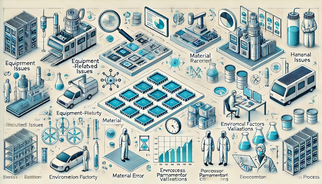
In the semiconductor manufacturing industry, yield is a critical metric that measures the efficiency and effectiveness of production processes. Yield refers to the proportion of functional chips produced from a semiconductor wafer. Understanding the various categories and factors that impact semiconductor yield is essential for optimizing production, reducing costs, and maintaining high product quality. This section will explore critical factors influencing semiconductor yield, ranging from defect density and process variability to advanced technological practices and future trends.
Category and Impact Factor
Description
Defect Density and Control
Defect density refers to the number of defects per unit area on a wafer, which can cause chips to be unusable.
Process Variability
Variations in temperature, pressure, and chemical concentrations during manufacturing can affect yield.
Equipment Reliability and Maintenance
Inconsistencies in machine performance, malfunctions, and wear and tear can disrupt the manufacturing process.
Material Quality and Purity
Variations in the quality and purity of raw materials, such as silicon wafers, can introduce defects.
Human Factors and Training
Human errors and differences in operator skills can impact yield.
Environmental Control
Environmental factors like cleanroom standards, humidity, and vibration control affect yield.
Design for Manufacturability (DFM)
DFM ensures products are designed with the manufacturing process in mind to enhance yield.
Advanced Lithography Techniques
Lithography involves using light to transfer patterns onto the wafer, where variations can cause defects.
Statistical Process Control (SPC)
SPC tools help monitor and control process variations to improve yield.
Yield Management Software and Analytics
Advanced software and data analytics are used to identify and address yield issues.
Future Trends in Yield Enhancement
Emerging trends such as AI, machine learning, and new materials promise future yield improvements.
Understanding the numerous factors that impact semiconductor yield is vital for any organization aiming to excel in the semiconductor industry. Manufacturers can significantly enhance yield rates by addressing issues such as defect density, process variability, equipment reliability, and material quality. Additionally, embracing advanced technologies and innovative practices will pave the way for future improvements in yield. By focusing on these critical areas, companies can achieve higher efficiency, reduced costs, and superior product quality, ultimately maintaining a competitive edge in the rapidly evolving semiconductor market.
How Will AI Impact Yield Detection And Improvement
As I conclude this exploration of the factors impacting semiconductor yield, one must highlight the transformative role of Artificial Intelligence (AI) in yield detection and improvement. AI is poised to revolutionize semiconductor manufacturing, providing advanced capabilities to enhance yield rates significantly.
Enhanced Defect Detection: AI-driven systems are highly efficient in identifying defects, surpassing traditional methods in accuracy and speed. Machine learning algorithms can sift through vast amounts of data from production processes to spot patterns and anomalies that may indicate defects. This real-time analysis enables immediate corrective actions, thereby reducing the number of defective chips and enhancing overall yield, providing a sense of reassurance about the quality of the products.
Predictive Maintenance: AI’s predictive capabilities can foresee equipment failures by analyzing data from sensors and maintenance logs before they occur. This proactive approach ensures that machinery operates at optimal performance levels, minimizing downtime and preventing defects caused by equipment malfunctions. Such proactive measures instill a sense of security about the reliability of the equipment and the stability of the manufacturing environment, which is crucial for high yield.
Process Optimization: AI algorithms are crucial in continuously monitoring and adjusting manufacturing processes to maintain optimal conditions. By analyzing data from various stages of production, AI can identify process variations and recommend adjustments to maintain consistency. This dynamic process control helps reduce variability, ensuring that each wafer meets the required standards for high yield.
Quality Control: AI enhances quality control by providing precise and consistent inspections. Automated visual inspection systems powered by AI can identify even the most minor defects that human inspectors might miss. This increased accuracy ensures that only high-quality chips progress through manufacturing, improving the overall yield.
Big Data Analytics: AI leverages big data analytics to provide insights into yield trends and potential issues. By aggregating and analyzing data from multiple production lines and facilities, AI can identify systemic problems and recommend solutions. This holistic view of the manufacturing process helps manufacturers implement best practices and continuously improve yield rates.
Take Away
Understanding the myriad factors that impact semiconductor yield is essential for optimizing production, reducing costs, and maintaining high product quality. Manufacturers can significantly enhance yield rates by addressing defect density, process variability, equipment reliability, and material quality issues. Embracing advanced technologies like AI and machine learning improves yield detection and defect management and drives continuous process optimization.
These innovations lead to higher accuracy in defect detection, proactive maintenance, and better quality control, ultimately resulting in more efficient and sustainable manufacturing practices. As the semiconductor industry continues to evolve, focusing on yield improvement will be vital to maintaining a competitive edge and meeting the growing demand for reliable, high-quality semiconductor products.
The semiconductor industry is a complex and highly competitive market, with companies constantly striving to reduce costs and improve efficiency. One key metric that semiconductor companies use to measure their performance is the Cost of Goods Sold (COGS), which represents the direct costs associated with producing and selling their products.
Let us examine the semiconductor COGS in more detail and identify the key components of this critical metric.
Key Components Of Semiconductor COGS
The critical components of the Semiconductor Cost of Goods Sold (COGS) include wafer cost, fab labor, fab overheads, equipment and tooling, materials and consumables, packaging and testing, yield losses, and inventory obsolescence. Below is the approximate breakdown of how each of these components contributes to the total cost of a given semiconductor product.
Component
Description
Percentage of COGS
Wafer Cost
Cost of silicon wafer used to produce semiconductor device
20-25%
Manufacturing Cost
Costs associated with manufacturing process (equipment, labor, overhead)
25-30%
Testing And Packaging Cost
Cost of testing and packaging semiconductor device
10-15%
Material And Labor Cost
Costs of raw materials and labor used in production process
10-15%
Overhead Cost
Indirect costs associated with production process (rent, utilities, administrative expenses)
5-10%
Note: The percentage ranges are approximate and may vary depending on the specific company and production process.
Various factors influence the semiconductor product cost structure, shaping the final COGS. Technological advancements are at the forefront, driving efficiencies and cost reductions through innovation. As semiconductor companies push towards smaller process nodes, the initial costs of new equipment and materials can be high. However, these investments often result in long-term savings and enhanced product performance. To stay ahead in the industry, exploring cost optimization strategies in response to these factors is crucial.
Economies of scale also significantly impact COGS. As production volumes increase, fixed costs are distributed across more units, reducing the cost per unit. This principle is especially relevant in an industry with high initial setup and production costs.
Geopolitical factors must also be considered, as they directly influence the availability and cost of raw materials and components. Tariffs, trade policies, and government incentives substantially determine operational costs. For example, subsidies and tax breaks can provide significant financial relief, making certain regions more attractive for manufacturing facilities.
Market demand and supply dynamics are equally critical and demand our attention. High demand can drive up prices for raw materials and manufacturing services. At the same time, supply chain disruptions, such as those caused by natural disasters or geopolitical tensions, can lead to shortages and increased costs. Adapting to these changing conditions is crucial to stay competitive in the market.
Take Away
Understanding COGS in the semiconductor industry is vital for students, professionals, and the industry. Mastering COGS is a crucial aspect of success in the semiconductor industry, impacting students, professionals, and the industry.
Group
Key Points
Students
Knowledge Foundation: Equip themselves with the ability to analyze and optimize production costs, including materials, labor, and overhead. Career Preparation: Prepare for roles that enhance manufacturing efficiency and drive innovation by understanding technological advancements and market dynamics.
Professionals
Enhanced Decision-Making: Improve decision-making and cost management in semiconductor manufacturing. Continuous Learning: Stay updated with industry trends, leverage advanced techniques, and engage in continuous learning to improve operational performance.
Industry In General
Competitiveness: Maintain competitiveness and profitability through effective COGS management. Cost Reduction: Achieve substantial savings by adopting innovative cost-reduction strategies and optimizing supply chains. Market Responsiveness: Respond effectively to market demands to ensure long-term success.
Each group can contribute to the industry’s growth and innovation by understanding and applying effective cost-management strategies. Continuous learning, strategic decision-making, and responsiveness to market demands will drive the future of semiconductor manufacturing, ensuring sustained competitiveness and profitability.
Semiconductor data is a vital yet costly resource. Unlike other data types, it requires significant financial investments to generate and maintain. Today, let us explore the economic impact of semiconductor data generation, supported by real-world examples and statistics.
What Is Semiconductor Data: It encompasses a wide range of information, including diffusion process data, assembly data, test data, and yield data. This data is essential for ensuring the quality, efficiency, and reliability of semiconductor products. For example:
Diffusion Process Data: Information on how materials are diffused in semiconductor wafers
Assembly Data: Details on the assembly of semiconductor components into final products
Test Data: Results from testing semiconductor devices to ensure they meet required specifications
Yield Data: Statistics on the number of functional devices produced from a batch of semiconductor wafers
Generating this data involves a series of complex and expensive processes. From setting up state-of-the-art fabrication plants (fabs) to conducting extensive research and development, the costs add up quickly.
For instance:
Aspect
Description
Setting Up Fabs
Building and equipping a semiconductor fab can cost billions of dollars. These facilities need to be equipped with cutting-edge technology and machinery to handle the intricate processes of semiconductor manufacturing.
Research And Development
RnD is a continuous and costly endeavor in the semiconductor industry. Developing new technologies and improving existing ones requires significant investment in talent, equipment, and time.
Testing And Quality Assurance
Ensuring that semiconductor products meet high standards of quality and reliability involves rigorous testing and quality assurance processes, which are both time-consuming and expensive.
Understanding The Economics Of Semiconductor Data
The generation of semiconductor data is not just a technical challenge but also a significant economic endeavor. The costs associated with obtaining high-quality data for semiconductor processes are immense, impacting both the industry and the broader economy. To understand this impact, it is essential to look at the financial investments required and the economic benefits that follow.
Statistics-Based Analysis:
Infrastructure Investment:
Intel in Chandler, AZ: Invested $32 billion, creating 3,000 jobs, for two new fabs. This highlights the significant upfront costs involved in setting up semiconductor manufacturing facilities.
TSMC in Phoenix, AZ: Invested $65 billion, creating 6,000 jobs, for three new fabs. This investment underscores the massive financial commitment required to expand semiconductor manufacturing capabilities.
Research And Development Costs:
According to a report by Semiconductor Industry Association (SIA), global semiconductor RnD spending reached approximately $71.4 billion in 2020. This demonstrates the continuous and substantial investment required for innovation and maintaining competitive advantage in the industry.
Testing And Quality Assurance:
The cost of testing and quality assurance in semiconductor manufacturing can account for up to 30% of the total manufacturing cost. This significant expenditure is necessary to ensure the reliability and performance of semiconductor products.
Connecting Expense With Yield Data Generation:
Yield Data Generation:
Yield data, which refers to the proportion of functional semiconductor devices produced from a batch of wafers, is critical for assessing and improving manufacturing processes.
Economic Impact:
Improved yield data can lead to higher production yields, reducing the cost per unit and increasing profitability. For instance, if a fab can increase its yield from 80% to 90%, it can produce more functional devices from the same number of wafers, enhancing overall efficiency and profitability.
Global Case Studies: Investments In Semiconductor Data
The global semiconductor industry is marked by substantial investments aimed at generating high-quality data essential for manufacturing and innovation. These investments vary across regions but consistently highlight the significant financial commitments required. Here, we delve into some global case studies, supported by statistical data, to illustrate the economic impact and strategic importance of these investments.
City
State
Company
Investment (Billion $)
Investment Type
Yield Data Context
Chandler
AZ
Intel
32
New (2 fabs)
Advanced manufacturing and process optimization
Phoenix
AZ
TSMC
65
New (3 fabs)
High-volume production, process stability
Fremont
CA
Western Digital
0.35
Expansion
Memory technology enhancement and scalability
Kissimmee
FL
SkyWater
Not Available
Expansion
Advanced packaging and integration
Boise
ID
Micron
25
New
Memory yield improvement and reliability
Taylor
TX
Samsung
17
New (1 fab)
Advanced logic chips and high performance
Sherman
TX
Texas Instruments
30
New (2 fabs)
Mixed-signal and analog technology
Malta
NY
GlobalFoundries
1
Expansion
Foundry services, process variability data
Syracuse
NY
Micron
100
New (4 fabs)
Large-scale memory and storage solutions
Columbus
OH
Intel
20
New (2 fabs)
Advanced semiconductor technology, high yield
These examples highlight the global scale and financial intensity of generating semiconductor data, essential for countries aiming to establish or enhance their semiconductor industries.
The Case For Open And Collaborative Semiconductor Datasets
The semiconductor industry stands at the forefront of technological innovation, yet it grapples with significant challenges related to data access and sharing. The high costs and proprietary nature of semiconductor data often hinder widespread research and development. This section explores the benefits of open and collaborative semiconductor datasets and how they can transform the industry.
Aspect
Details
Enhancing Innovation And Research
– Accelerated Development: Sharing data speeds up technological advancements.
– Cross-Disciplinary Insights: Enables collaboration across fields for innovative solutions.
Reducing Costs And Redundancy
– Economies of Scale: Spreads the cost of data generation across a broader base.
– Avoiding Duplication: Prevents redundant data collection, saving time and resources.
Improving Data Quality And Reliability
– Peer Review and Validation: Wider scrutiny improves data accuracy and reliability.
– Standardization: Leads to consistent and easy-to-use data formats.
Fostering Global Competitiveness
– Leveling the Playing Field: Democratizes innovation by making data accessible to all.
– Enhancing National Security: Reduces dependency on foreign data and technology.
Case Studies And Examples
– DARPA’s ERI: Encourages collaboration and data sharing for advancements in electronics.
– Open Compute Project: Demonstrates rapid innovation and cost reduction through open collaboration.
Challenges And Considerations
– Intellectual Property Concerns: Balancing data sharing with protecting competitive advantage.
– Data Security: Ensuring the security and integrity of open datasets.
– Incentive Structures: Developing frameworks to encourage data sharing while protecting commercial interests.
Take Away
The semiconductor industry is both a cornerstone of technological innovation and a domain with immense economic implications. Generating the necessary data for semiconductor manufacturing is a costly and complex endeavor, requiring substantial investments in infrastructure, research, and quality assurance. Despite these high costs, semiconductor data is essential for ensuring product quality, efficiency, and competitiveness.
Understanding the hidden costs and economic impact of generating semiconductor data is crucial for stakeholders. By embracing open access and collaborative approaches, the semiconductor industry can overcome financial barriers, drive innovation, and achieve sustainable growth. This strategic approach will benefit not only the industry but also the broader technological landscape, paving the way for future breakthroughs and economic prosperity.
Semiconductor yield, the percentage of functional chips produced from a wafer, is a critical factor in the semiconductor industry. Yield influences production’s cost efficiency and determines manufacturing operations’ overall economic viability.
High yield directly impacts various economic aspects, including cost per chip, profit margins, market competitiveness, investment in technology, and supply chain efficiency.
Let us explore these implications from a product perspective, providing a comprehensive understanding of how yield affects the broader semiconductor landscape.
Key Metrics For Semiconductor Yield Analysis
As a first step, yield analysis involves understanding the percentage of functional chips produced from a wafer and identifying the factors influencing this outcome. By leveraging key metrics, manufacturers can gain insights into their production processes’ effectiveness, identify improvement areas, and make informed decisions to enhance yield performance.
This analysis improves the technical aspects of manufacturing and has profound financial implications, impacting profitability, cost management, and overall competitiveness. This section delves into the essential metrics used in semiconductor yield analysis, explaining their definitions, importance, and practical applications.
Die Yield: Die yield is the percentage of functional dies (chips) on a wafer. It measures the effectiveness of the manufacturing process. A high die yield indicates fewer defects and greater efficiency, leading to lower costs and higher profitability.
Defect Density (D0): Defect density is the number of defects per unit area on the wafer. Lower defect density indicates a cleaner manufacturing process and higher yield potential. It is an essential metric for assessing the quality of the production environment and processes.
Overall Yield: Overall yield considers multiple manufacturing stages and their yields. This metric provides a comprehensive view of the entire production process’s effectiveness. It highlights the importance of optimizing each stage to achieve a high yield, ensuring consistent and efficient production.
First-Pass Yield (FPY): Measures the percentage of products that pass all manufacturing stages without rework or repair. It is an indicator of process efficiency and quality. A high FPY reflects a well-optimized manufacturing process with minimal defects and interruptions, reducing production costs and faster time to market. Monitoring FPY helps identify areas in the production process that may need improvement to enhance overall yield and product quality.
Yield Model: Murphy’s model predicts yield based on defect density and die area. This model helps understand the relationship between defect density and yield, which helps make informed decisions about process improvements and defect reduction strategies.
Gross Die Per Wafer (GDW): Gross die per wafer is the total number of dies that can be produced from a single wafer. This metric helps estimate the potential production volume based on the wafer’s diameter and the area of a single die. It is crucial for planning manufacturing capacity and understanding production limits.
Critical Area Analysis: Critical area analysis estimates the yield loss due to defects in specific die areas. Manufacturers can target improvements more effectively by identifying and addressing critical areas where defects can cause failures. This analysis is vital for optimizing design and manufacturing processes to enhance yield.
Return On Investment (ROI): Measures the profitability of an investment relative to its cost. In semiconductor manufacturing, ROI is calculated for investments in new technology, equipment, or process improvements. A higher ROI indicates that the investment has generated significant returns, justifying the expenditure.
Gross Margin: Gross margin is the difference between revenue and the cost of goods sold (COGS), expressed as a percentage of revenue. It indicates the efficiency of the manufacturing process and the product’s profitability. Higher gross margins reflect better cost control and higher profitability.
Yield To Cost (YTC): Measures the relationship between yield improvements and cost reductions. It assesses how changes in yield affect overall production costs. A positive YTC indicates that yield improvements effectively reduce costs and enhance profitability.
Cost Per Die: Total manufacturing cost divided by the number of functional dies produced. This metric helps understand the cost efficiency of the manufacturing process. Lower CPD indicates higher efficiency and better cost management.
Break-Even Yield: The yield percentage of total revenue equals total production costs, resulting in neither profit nor loss. Understanding BEY is crucial for setting yield targets that ensure profitability. Achieving yields above BEY ensures that the manufacturing process is profitable.
To fully grasp the economic implications of semiconductor yield, analyzing how yield improvements influence different aspects of semiconductor production and their subsequent effects on the market is essential. The table below highlights the primary areas affected by yield and provides examples to illustrate these impacts:
Aspect
Details
Implication
Cost Per Chip
Reduces manufacturing costs by lowering per-unit cost through higher yield. Achieves economies of scale, enabling competitive pricing.
A 1% yield improvement can save millions for smartphone manufacturers.
Profit Margins
Enhances profitability by increasing the number of sellable units per wafer. Improves gross margins, supporting financial stability.
Minor yield improvements can significantly boost profits in high-value processors.
Market Competitiveness
Balances price and performance, attracting cost-conscious consumers. Ensures performance consistency, differentiating in premium segments.
High yields allow consumer electronics brands to deliver high-performance, competitively-priced devices.
Investment In Technology
Justifies significant RnD investments, driving innovation. Ensures sustainable growth by maintaining high yields.
Investments in advanced technologies support high yields and industry leadership.
Supply Chain Efficiency
Leads to predictable production outputs, facilitating better planning. Optimizes inventory, reducing excess stock and avoiding shortages.
High yield ensures a steady supply of chips, crucial for just-in-time production models.
As demonstrated in the above table, each aspect of semiconductor yield significantly impacts the economic dynamics of semiconductor manufacturing. High yield is a crucial driver of financial success in the industry, from reducing the cost per chip to enhancing supply chain efficiency.
Importance of Modeling in Semiconductor Yield Analysis
Modeling provides a framework for predicting, analyzing, and optimizing yield, offering significant advantages in various aspects of semiconductor manufacturing. The table below focuses on the critical benefits of modeling in yield analysis and includes illustrative examples and case studies.
By leveraging advanced modeling techniques, semiconductor manufacturers can significantly enhance their yield performance, driving economic success and maintaining market competitiveness.
Aspect
Details
Impact
Accurate Yield Predictions
Predicts yield outcomes based on process parameters and defect rates, aiding in informed decision-making.
Using statistical models to estimate yield in wafer production improves forecasting accuracy.
Process Optimization
Simulates different process conditions to identify optimal settings that maximize yield and minimize defects.
Modeling optimal etching parameters in semiconductor fabrication to enhance yield.
Defect Analysis And Mitigation
Understands the relationship between defects and yield loss, enabling targeted defect mitigation strategies.
Analysis of critical defects in photolithography processes, leading to improved cleanroom protocols.
Cost Reduction
Identifies yield-limiting factors early, avoiding costly rework, scrap, and downtime, thus reducing production costs.
Early detection of yield issues in chip packaging, saving costs associated with rework and scrap.
Innovation And Development
Provides a virtual testing ground for new technologies and processes, accelerating the development cycle.
Simulation of new materials in transistor design, reducing time-to-market for advanced technologies.
Risk Management
Assesses potential risks of yield fluctuations and develops contingency plans to ensure stable production outputs.
Risk assessment models for managing yield variability in high-volume semiconductor manufacturing.
Continuous Improvement
Regularly updates models with new data to refine yield dynamics understanding, driving higher performance over time.
Ongoing improvement in yield prediction models for dynamic random-access memory (DRAM) production.
Predictive Modeling
Forecasts yield outcomes based on wafer inspection data, allowing for preemptive corrective actions.
Use of machine learning algorithms in memory chip production to predict and mitigate yield issues.
Take Away
The economic implications of semiconductor yield are profound, affecting cost per chip, profit margins, market competitiveness, investment in technology, and supply chain efficiency. High yield is essential for maintaining competitive pricing, enhancing profitability, driving innovation, and ensuring supply chain stability.
As technology advances, semiconductor manufacturers will continue to prioritize higher yields. Ongoing improvements in manufacturing processes, defect detection, and technological innovation will drive the industry’s growth and economic viability, ensuring that semiconductor yield remains a critical determinant of success.
Semiconductor Product Development And Yield Correlation
The semiconductor industry continually innovates and introduces new products to meet the growing demands for more powerful and efficient electronic devices. The successful launch of these new semiconductor products always hinges critically on yield.
As such, yields are not just a statistic in semiconductor terminology. They impact the production costs per usable chip, which can significantly affect profit margins, particularly in a highly competitive market with limited pricing power.
From A Semiconductor Product Perspective: Yield is considered after the chip has been fabricated, assembled, and tested. It involves the proportion of chips that function correctly and meet the desired performance specifications. This aspect of yield is crucial because it determines the compliance, quality, and eventually the profitability of the new semiconductor product.
Moreover, the correlation between yield and the broader semiconductor industry extends to how companies manage their supply chains and respond to market demands. Thus, a stable and high yield is crucial for maintaining reliable product supply, affecting market share and consumer confidence.
Eventually, effective yield management will support cost efficiency, product quality, strategic positioning, and competitive advantage in the semiconductor landscape.
Setting And Achieving The Target Yield
Setting the target yield in semiconductor product development is a critical strategic decision that balances technical feasibility with business goals. Companies often set this target based on historical yield data, technology (node) used, product complexity, and defectivity to anticipate and mitigate potential production to cost challenges.
“What Is Target Yield? Refers to the predefined goal for the percentage of functional units produced from a batch of semiconductor wafers. Semiconductor companies set a target yield to measure the efficiency and effectiveness of their products and processes. Setting a target yield is vital for several reasons, including cost control, production planning, and ensuring the economic viability of manufacturing operations.”
On other hand, achieving yield targets is a multifaceted process that involves a series of detailed and strategic testing stages. Each stage addresses different aspects of a semiconductor’s functionality and performance, progressively ensuring that yield targets are verified and, if not met, then the product is improved through another silicon revision by root causing the issue.
Below are the different testing methods that are used to validate the semiconductor product and the yield:
Stage
Description
Impact on Yield
Simulation-Based Testing
Utilizes advanced computational models to predict how a semiconductor device will behave under various physical, electrical, and environmental conditions before actual physical testing begins. It helps identify potential issues before they manifest in real-world scenarios.
It improves yield by enabling early detection of design flaws and operational shortcomings, reducing the need for costly physical reiterations.
Bench Testing
Initial assessment of each chip under controlled conditions to verify it meets fundamental design specifications.
Lays the groundwork for higher yield rates by identifying and correcting early design discrepancies.
Application Testing
Tests the chip within its specific intended application (e.g. a computer processor) to evaluate performance in operational environments.
Boosts yield by refining design and manufacturing processes to reduce application-specific failures.
System-Level Testing
Integrates the chip with other hardware and software to ensure compatibility and meeting performance metrics across a system.
It is identifying integration issues that might affect yield, such as electric interference and data throughput issues.
Assembly/Packaging
It involves encapsulating the die in a protective casing and testing for physical, thermal, and chemical resilience.
Ensures mechanical and environmental robustness, directly influencing yield concerning product longevity and failure rates.
Test/Automatic Test Equipment (ATE)
Simulates real-world operating conditions to test the chips for quality and durability rigorously.
Minimizes late-stage production failures, achieving high yield by ensuring readiness and reliability under operational specifications.
Quality Control
Testing all manufacturing process aspects to adhere to stringent quality standards.
Maintains high yield rates by ensuring consistent quality across production batches and over time.
Reliability Testing
Focuses on the long-term performance of the chips, predicting and improving life expectancy and failure rates.
Enhances yield rates by identifying late-life failures, which is crucial for customer satisfaction.
In the semiconductor industry, the Cost of Goods Sold (COGS) encompasses various elements such as fabrication, assembly, testing, material costs, direct labor costs, and other overheads. However, the one factor that truly holds the power to influence the product margin, driven by COGS, is yield. Thus, reduction or increasing in the number of good products per wafer (i.e. yield) impacts manufacturing costs (COGS), making it a crucial aspect to consider.
Below is a view of how achieving a target yield helps with lower COGS and the production of a product:
Impact On COGS: Improved yields directly lead to lower COGS as the effective utilization of inputs (materials, labor, and capital) increases. It is crucial in the semiconductor industry, where price erosion is common, and the ability to rapidly reduce costs can be a significant competitive advantage.
Pricing Flexibility: Lower COGS allows greater flexibility in pricing its products. It can be critical in competitive markets or when companies seek to penetrate new markets by underpricing competitors without sacrificing margins.
Profitability: Lower COGS resulting from higher yields boosts gross margins, a key indicator of production efficiency and profitability. In a capital-intensive industry like semiconductors, where initial investments and fixed costs are high, maximizing yield is often synonymous with maximizing profitability.
Inventory Management: Higher yields can lead to more consistent production outputs, which helps better inventory management. Companies can reduce the buffer stocks they might otherwise hold to compensate for potential yield variability, thus minimizing the costs associated with holding inventory.
Eventually, companies that excel in yield optimization improve their operational efficiencies and strengthen their financial (where COGS is crucial) position, providing more stability in the volatile semiconductor market.
Semiconductor Yield Take Away
By now, it is obvious how important the yield is in validating new semiconductor products. Yield also influences several aspects of a semiconductor company’s operations, from financial stability to market competitiveness.
To summarize, here are four key takeaways on how crucial yield is during the validation phase of new semiconductor products:
Cost Efficiency And Profitability:
Yield directly impacts the cost efficiency of semiconductor manufacturing. Higher yields mean more functional devices are produced per batch, reducing the per-unit cost of production. This cost-saving is crucial when scaling up production for market launch.
Effective yield management during the validation phase can dramatically enhance profitability by minimizing waste and optimizing resource use, setting a solid foundation for competitive pricing and healthy profit margins as the product enters the market.
Product Quality Add Reputation:
Achieving a high yield is synonymous with ensuring product quality during validation. High yield indicates that the manufacturing processes can consistently produce devices that meet or exceed specifications.
This strengthens customer trust and satisfaction and enhances the product’s reputation for reliability. A high yield during product validation can thus serve as a quality assurance marker, reassuring stakeholders and customers about the product’s performance and durability.
Time To Market And Competitive Advantage:
Yield optimization during validation affects a company’s agility and speed in bringing new products to market. High yield rates allow for a smoother transition from development to full-scale production, reducing delays caused by extensive troubleshooting and reiterations.
This speed to market is a crucial competitive advantage, especially in a fast-paced industry like semiconductors, where being first can dictate market leadership and capture significant market share.
Supply Chain Stability And Responsiveness:
High yields during the validation phase contribute to supply chain stability by ensuring production volumes meet forecasted demands. This stability is crucial for maintaining consistent customer supply and responding flexibly to market demand changes.
Moreover, predictable and stable yields reduce the risk of stockouts and excess inventory, thus optimizing the supply chain operations and reducing logistical costs.
In conclusion, yield must be considered critical when designing, manufacturing, and validating new semiconductor products. More so, when yield touches every essential aspect of a semiconductor company’s operations – from cost structure and product quality to market positioning and supply chain management.
In the long term, effective yield management during product validation is a strategic imperative that underpins operational efficiency and the long-term success of a product in the semiconductor industry.
Understanding The Semiconductor Industry Landscape: A Workforce Perspective
The semiconductor industry is dynamic and rapidly evolving, offering a wide array of career opportunities for a skilled workforce. With the global market projected to reach $1 trillion by 2030, the demand for talent is growing, particularly in regions like Asia-Pacific, North America, and Europe.
For students and early career professionals, understanding this landscape means recognizing the importance of specialized education, hands-on experience, and continuous skill development. The industry values technical expertise and prioritizes problem-solving abilities, effective communication, and teamwork. By staying informed about industry trends and investing in their professional growth, aspiring engineers can position themselves for success in this essential and ever-expanding sector.
Among the various workforce roles in the semiconductor industry, quality and reliability engineers stand out as one of the most critical. These professionals are the backbone of the industry, ensuring that semiconductor devices meet stringent quality standards and perform reliably over their intended lifespan.
Quality engineers focus on detecting and eliminating defects during manufacturing, ensuring that each chip adheres to precise specifications. On the other hand, reliability engineers work on predicting and enhancing the long-term performance of these devices, conducting stress tests, and performing in-depth failure analysis.
For students and early career professionals, specializing in quality and reliability engineering offers a robust career path with significant impact, as these roles are integral to the advancement and sustainability of semiconductor technology.
Focus On Quality And Reliability
Quality and reliability engineers ensure that semiconductor products meet strict quality standards during production and perform reliably throughout their intended lifespan. As the complexity and demand for advanced semiconductor devices increase, the expertise of quality and reliability engineers becomes increasingly vital.
Quality: Quality assurance (QA) ensures that semiconductor products meet predefined standards and specifications at various stages of production. It involves rigorous testing and inspection processes to identify and eliminate defects, ensuring that each chip performs as intended before it reaches the customer.
Reliability: Reliability engineering goes beyond initial quality assurance to ensure that semiconductor devices perform consistently over their expected lifespan. It involves understanding and mitigating failure mechanisms, conducting stress tests, and predicting long-term performance under various operating conditions.
Their work underpins the industry’s ability to deliver high-performance, durable products, thereby maintaining customer trust and supporting the continuous innovation that drives the semiconductor market forward. Let us delve deeper into the importance of quality and reliability in semiconductors and explore the career opportunities in these specialized fields.
Responsibilities Of A Quality And A Reliability Engineer
While their ultimate goals align with producing high-quality, dependable devices, their responsibilities and focus areas differ significantly. Understanding these differences is crucial for students and early career professionals specializing in either field.
Aspect
Quality Engineer
Reliability Engineer
Primary Focus
Ensuring products meet predefined standards and specifications at various stages of production.
Ensuring products perform reliably over their intended lifespan and under various operating conditions.
Standards Compliance
Ensure adherence to industry standards (IEC, JEDEC, AEC etc.) and regulatory requirements to guarantee product quality.
Ensure compliance with reliability standards (IEC, JEDEC, AEC etc.) and perform reliability modeling and simulation.
Yield Rate
Focus on maximizing yield rate by minimizing defects and ensuring a high percentage of functional chips.
Not directly involved in yield rate but focus on ensuring long-term reliability of the functional chips produced.
Failure Analysis
Not typically involved in detailed failure analysis beyond initial defect detection.
Conduct in-depth failure analysis to understand root causes of device failures and develop corrective actions.
Predictive Modeling
Not typically involved in predictive modeling for product performance.
Use predictive modeling to estimate the long-term reliability and service life of semiconductor devices.
Customer Feedback
Handle customer returns and feedback to identify quality issues and improve manufacturing processes.
Analyze field data and customer feedback to identify reliability issues and improve product designs.
Tools and Techniques
Use tools such as Six Sigma, SPC (Statistical Process Control), and automated testing equipment.
Use tools such as FMEA (Failure Mode and Effects Analysis), reliability software (e.g., ReliaSoft), and statistical modeling.
Team Collaboration
Work closely with manufacturing and design teams to implement quality control measures and resolve defects.
Collaborate with design, manufacturing, and quality teams to ensure products meet reliability standards and perform failure analysis.
How Students Can Gain Skills To Become Quality and Reliability Engineers
Acquiring the skills necessary to become a quality or reliability engineer in the semiconductor industry involves a strategic blend of education, hands-on experience, and continuous learning. Students should start by pursuing relevant electrical engineering, materials science, or computer engineering degrees.
Education Wise:
Method
Description
Pursue Relevant Degrees
Degrees in Electrical Engineering, Materials Science, Computer Engineering, or Mechanical Engineering provide essential knowledge.
Specialized Courses
Courses in Semiconductor Device Physics, Quality Management, and Reliability Engineering enhance specific skills.
Specialized courses in semiconductor device physics, quality management, and reliability engineering will provide a deeper understanding of the principles and practices in these areas.
Skill Wise:
Method
Description
Proficiency with Tools and Software
Learn to use quality tools (Six Sigma, SPC), reliability tools (FMEA, ReliaSoft), and design software (CAD).
Data Analysis
Develop skills in statistical analysis and predictive modeling for semiconductor performance and reliability.
Practical experience gained through internships and co-op programs with semiconductor companies is invaluable, as it offers hands-on exposure to manufacturing processes, quality control, and reliability testing. Participating in university research projects or collaborating on interdisciplinary projects can enhance practical knowledge and problem-solving abilities.
Takeaway
A multifaceted approach to skill development is essential for students aspiring to become quality or reliability engineers in the semiconductor industry. Pursuing relevant educational pathways, gaining hands-on experience through internships, and participating in research projects lay the groundwork for technical proficiency. Acquiring certifications and continuously learning through workshops and online courses will keep you abreast of industry advancements.
Finally, developing solid and soft skills such as communication, teamwork, and analytical thinking will enable you to effectively contribute to interdisciplinary teams and solve complex challenges. By strategically combining these elements, you can build a robust foundation for a successful career in ensuring the quality and reliability of semiconductor devices.
The semiconductor industry is the backbone of modern technology, powering everything from smartphones to advanced computing systems. In 2022 alone, the global semiconductor market was valued at over $500 billion and projected to reach $1 trillion by 2030, driven by advancements in artificial intelligence and edge devices.
As the semiconductor industry continues to expand rapidly, the need for skilled professionals in semiconductor manufacturing is becoming increasingly urgent. A Semiconductor Industry Association (SIA) report predicts that the sector will require an additional 1 million skilled workers by 2030 to keep up with production and innovation demands, presenting a significant opportunity for those considering a career in this field.
Below is the guide for students approaching the available semiconductor manufacturing courses, helping them make informed decisions about their education and career paths.
STEP 1: Understanding Semiconductor Manufacturing
Before taking specific courses, students must have a solid understanding of semiconductor manufacturing. This step provides the foundational knowledge necessary to grasp the complexity and precision involved in creating semiconductor devices.
Semiconductor manufacturing includes photolithography, etching, doping, and packaging, each requiring high accuracy and technological expertise. By comprehending these fundamental processes, students can better appreciate the intricate work behind the chips that power modern technology.
Resources such as textbooks, online courses, and industry publications are excellent starting points for building this foundational knowledge. Additionally, understanding the historical evolution of semiconductor manufacturing, from the invention of the transistor to the development of modern microprocessors, can provide context and highlight the industry’s innovative nature.
While understanding the historical context is important, it is equally vital for students to familiarize themselves with the industry’s current state. This includes knowing the major players, significant technological advancements, and ongoing research and development efforts. This broad overview will equip students with the necessary background to make informed decisions about their education and career paths in semiconductor manufacturing.
STEP 2: Research Semiconductor Manufacturing Skill Demand
Understanding the demand for specific skills in semiconductor manufacturing is the first critical step for any student considering a career in this field. The semiconductor industry is highly dynamic, with continuous advancements requiring new competencies and expertise. By researching the current and future skill demands, students can align their educational pursuits with market needs, increasing their employability and career prospects.
Students should start their journey by delving into the wealth of industry reports, such as those published by the Semiconductor Industry Association (SIA) or consulting firms like McKinsey & Company. These reports provide invaluable insights into emerging trends and technologies, equipping students with the knowledge they need to make informed career choices and stay ahead of the curve.
Example Of Skill Demand Analysis: High-demand skills include expertise in photolithography, chemical vapor deposition (CVD), and atomic layer deposition (ALD). Additionally, knowledge of advanced packaging technologies like 2.5D and 3D integration is increasingly valuable. According to industry reports, there is a growing need for professionals who can work with emerging materials and fabrication techniques.
Pinpointing high-demand skills is a great start, but it is about more than just the skills. It is about understanding the context and real-world applications. To truly immerse yourself in the semiconductor manufacturing world, engaging with industry professionals is essential. Seminars, webinars, and professional organizations are a goldmine of insights into skill requirements, and they also provide a sense of community and connection, making you feel part of something bigger.
It is crucial to stay updated with the semiconductor industry’s ever-evolving needs. One effective way to do this is by exploring job postings and internship opportunities, which can provide a clear understanding of the qualifications and experiences employers seek. This foundational research can guide course selection and assist students in building a robust and relevant skill set.
Lastly, the prospects of skills are also significant. The future of semiconductor manufacturing will likely see a greater emphasis on sustainability and energy efficiency. Skills in developing low-power semiconductor devices and sustainable manufacturing practices will be highly sought, opening up a world of possibilities. Furthermore, the rise of quantum computing and neuromorphic engineering presents new opportunities and challenges, requiring a new generation of semiconductor experts.
STEP 3: Types Of Semiconductor Manufacturing Courses
Once students have a solid understanding of semiconductor manufacturing, the next step is to explore the various courses available. This section will guide students through different specializations within the field, each offering unique career opportunities.
Courses in fabrication (fab) processes cover essential manufacturing techniques, while design and simulation courses focus on creating and optimizing semiconductor circuits. Packaging and testing courses delve into the final stages of production, ensuring device reliability and performance.
Below is the information in a table format for better presentation. This table format provides a clear and organized presentation of the different types (limited list) of semiconductor manufacturing courses, along with their content, skills acquired, and related career opportunities, ensuring you can easily navigate and understand the information, and feel at ease in your decision-making process.
Course Type
Course Content
Skills Acquired
Career Opportunities
Fabrication (Fab) Process Courses
Photolithography, chemical vapor deposition (CVD), etching, doping, planarization
Cleanroom protocols, process optimization, equipment operation
Process engineer, equipment technician
Design And Simulation Courses
VLSI design, CAD tools, simulation techniques
Circuit design, system simulation, CAD tool proficiency
Material science and semiconductor physics courses provide a deep dive into the properties and behaviors of semiconductor materials. Additionally, courses in equipment operation, data analytics, new device development, silicon wafer processing, and cleanroom management and safety offer specialized skills tailored to specific industry needs.
Understanding the content, skills acquired, and career opportunities associated with each type of course is crucial. However, it is equally essential for students to consider their interests and strengths. This comprehensive overview is a guide and a compass that can help students navigate the semiconductor industry’s vast landscape, identify the most relevant and valuable courses for their career aspirations, and reduce confusion in course selection.
STEP 4: Selecting The Right Semiconductor Manufacturing Course
Choosing the right semiconductor manufacturing course is a crucial decision that can significantly impact a student’s career trajectory. This step involves assessing personal interests, strengths, and career goals to select courses that offer the best fit.
Students should consider their passion for specific aspects of semiconductor manufacturing, whether it’s hands-on fabrication, theoretical design, material science, or data analytics. Evaluating industry demand and trends is also essential. Selecting courses aligned with high-demand skills ensures better job prospects upon graduation.
Students should research institutions and programs, prioritizing those with solid reputations and accreditation, as these often provide superior education quality and networking opportunities. Additionally, seeking advice from academic advisors, industry professionals, and alums can provide valuable insights into the best courses and institutions.
By carefully evaluating these factors, students can make informed decisions that enhance their educational experience and prepare them for successful careers in the semiconductor industry. This step ensures that students gain relevant knowledge and skills and position themselves strategically in a competitive job market.
STEP 5: Connecting The Semiconductor ManufacturingKnowledge To Applications
Applying semiconductor manufacturing knowledge in real-world scenarios is critical for career success. This step encourages students to bridge the theoretical learning and practical application gap. Courses often provide foundational knowledge, but applying this knowledge in industry settings through internships, projects, and hands-on training is invaluable.
Real-world applications of semiconductor manufacturing knowledge are not just about developing new devices, optimizing processes, or implementing quality control measures. They are about students seeing how their skills, honed through theoretical learning and practical experiences, contribute to innovative solutions and technological advancements. Networking and industry events further enrich their understanding of the current challenges and opportunities in semiconductor manufacturing.
Studying case studies and success stories of professionals in the field is a valuable source of inspiration and guidance for students. This step underscores the importance of experiential learning and continuous professional development. It equips students with the necessary tools to tackle real-world problems and contribute meaningfully to the semiconductor industry.
STEP 6: Plan For Re-Skilling And Up-Skilling
The semiconductor industry is continuously evolving, and staying relevant requires a commitment to lifelong learning. This step focuses on planning for re-skilling and up-skilling to keep pace with technological advancements. Students and professionals should regularly assess their skill sets, identify gaps, and seek further education and training opportunities.
This might involve taking advanced courses, obtaining new certifications, or attending workshops and seminars. Many semiconductor companies offer training programs to help employees stay updated with the latest technologies and practices. Additionally, online platforms and educational institutions provide flexible learning options that can accommodate busy schedules. Networking with peers and industry experts, joining professional organizations, and participating in industry conferences can also enhance learning and professional growth.
Students can ensure they remain competitive and valuable assets in the semiconductor industry by developing a long-term career development plan that includes goals for acquiring new skills and knowledge. This proactive approach to continuous learning is not just a necessity, but a powerful tool for adapting to the ever-changing landscape of semiconductor manufacturing, inspiring you to take charge of your professional journey.
Take Away
Ultimately, the semiconductor manufacturing field offers many opportunities for students. By understanding the different types of courses available and conducting a thorough self-assessment of their interests and strengths, students can make informed decisions that are in perfect harmony with their career goals.
Students should always research first and then enroll in relevant semiconductor manufacturing courses that match their career aspirations.
India’s semiconductor industry is on the cusp of a significant transformation, driven by a huge demand for talent and rapid technological advancements. With 2.55 million STEM graduates yearly, India ranks second globally in producing Science, Technology, Engineering, and Mathematics graduates.
As the world increasingly relies on semiconductors for everything from smartphones to electric vehicles, India’s role as a key player in this global ecosystem becomes increasingly critical.
Thus, exploring the multifaceted dynamics of the demand for semiconductor talent in India is essential, shedding light on the historical context, current landscape, and the factors fueling this demand.
Semiconductor Background In India
India’s journey in the semiconductor industry began in the late 20th century, marked by the establishment of key research institutions and the advent of multinational semiconductor companies setting up operations in the country. Initially, India’s role was primarily confined to software services and design, leveraging its strong IT industry.
Over the years, however, the landscape has evolved. Government initiatives, such as the Make in India campaign and semiconductor fabrication labs’ establishment have been pivotal in fostering a more comprehensive semiconductor ecosystem. Today, India is a hub for semiconductor design and makes strides in manufacturing and research, positioning itself as a critical player in the global supply chain.
STEM Graduates In India
India is a powerhouse in STEM education, with more than 2.55 million graduates yearly, second only to China. This significant pool of STEM talent positions India as a crucial player in the global semiconductor industry. The abundance of skilled graduates from Indian universities ensures a steady supply of engineers, researchers, and technicians to fuel the semiconductor sector’s growth.
India’s prominence in STEM education underpins its potential to address the global semiconductor talent shortage. As the industry evolves with advancements in AI, the demand for highly specialized knowledge and skills increases. Indian STEM graduates, equipped with strong technical backgrounds, are thus well-suited to meet these needs, driving innovation and efficiency in semiconductor design and manufacturing.
Moreover, India’s educational institutions and government initiatives foster an environment conducive to technological advancements. Partnerships between academia and industry, alongside government incentives, are crucial in enhancing the skill sets of Indian STEM graduates, making them even more valuable to the semiconductor industry.
In the near-term, India’s substantial number of STEM graduates will play a pivotal role in the semiconductor sector. Leveraging this talent pool can significantly impact global semiconductor supply chains, ensuring sustained innovation and competitiveness in this critical field.
Factors Driving Semiconductor Growth In India
Understanding the factors driving the demand for semiconductor talent in India is crucial to appreciating the industry’s growth dynamics. Government initiatives, which are significant, market growth, which is promising, technological advancements, and the push for self-reliance are all playing pivotal roles in shaping this demand.
These elements collectively create a fertile ground for the semiconductor sector to flourish, necessitating a diverse and skilled workforce.
Factor
Description
Government Initiatives
Policies such as the Production Linked Incentive (PLI) scheme and Electronics Manufacturing Clusters (EMC) scheme aim to attract investments and boost local production capabilities, fostering a conducive environment for semiconductor companies.
Market Growth
The global semiconductor market is expanding due to the proliferation of digital technologies like AI. This growth increases the demand for skilled professionals to design and manufacture semiconductors.
Technological Advancements
Emerging technologies require advanced semiconductor solutions, driving the need for highly skilled workers. Indian educational institutions are focusing on these technologies, producing graduates equipped to meet industry needs.
Self-Reliance
Efforts to reduce dependency on foreign semiconductor imports and enhance local capabilities drive demand for skilled talent. Initiatives to promote domestic semiconductor manufacturing and design are crucial in achieving self-reliance.
Understanding the areas where talent demand is most pronounced in the semiconductor industry is paramount. By delving into the various domains – design, manufacturing, and RnD – one can pinpoint the skills and expertise in high demand.
This detailed examination will highlight the critical roles and opportunities available, shedding light on how India’s educational institutions and industry partnerships prepare to meet these demands.
Section
Details
Areas Of Talent Demand
Design: Demand for roles such as design engineers, verification engineers, and system architects has surged, driven by AI and computing advancements. Manufacturing: Rising demand for process engineers, equipment engineers, and technicians due to government initiatives and new fab setups. RnD: High demand for materials science, quantum computing, and nanotechnology researchers to drive innovation.
Education And Skill Development
Educational Institutions: Premier institutions like IITs, NITs, and leading universities offer specialized electronics and engineering programs. Skill Gaps: Additional training in VLSI design, semiconductor fabrication, and advanced materials science is needed. Industry-Academia Collaboration: These partnerships, fostering sponsored research, internships, and workshops, are key to aligning academic programs with the dynamic needs of the industry, leading to a more skilled workforce.
Challenges
Brain Drain: The migration of skilled professionals abroad for better opportunities; the need to create attractive work environments in India. Infrastructure: There is a need for substantial investment in advanced machinery and facilities for semiconductor fabs and research labs. Retention: Competitive salaries, a positive work culture, continuous learning, and clear career progression are essential to retain talent.
Opportunities And Future Outlook
Startups and Innovation: Emergence of startups focusing on AI, IoT, and specialized semiconductor applications, supported by government initiatives. Global Competitiveness: The industry’s strength lies in its ability to leverage highly skilled professionals, a robust education infrastructure, and unwavering government support, all of which are propelling it towards becoming a semiconductor global leader. Long-term Strategies: The industry is committed to a path of continuous investment in education, infrastructure, and industry collaboration, bolstered by policies that foster innovation and ease of doing business.
Take Away
For sure, India is pivotal in the global semiconductor industry, driven by a robust educational infrastructure, supportive government policies, and a market demand. The nation’s significant pool of STEM graduates positions it to meet the growing global and domestic demand for semiconductor talent. However, challenges such as brain drain, infrastructure limitations, and retention issues must be addressed to fully capitalize on this potential.
By fostering solid collaborations between industry and academia, investing in advanced training programs, and creating a conducive work environment, India can bridge the existing skill gaps and enhance its competitiveness on the global stage. The rise of startups and innovation hubs, supported by government initiatives, further underscores the country’s potential to lead in semiconductor design, manufacturing, and RnD.
Long-term strategies focusing on continuous investment in education, infrastructure, and policy support are essential to sustain and grow the semiconductor talent pool. As India navigates these challenges and opportunities, it is well-positioned to become a global powerhouse in the semiconductor industry, driving innovation and economic growth for years.