Category: TESTING

  • The Semiconductor DFT Approach That Shapes IC Reliability

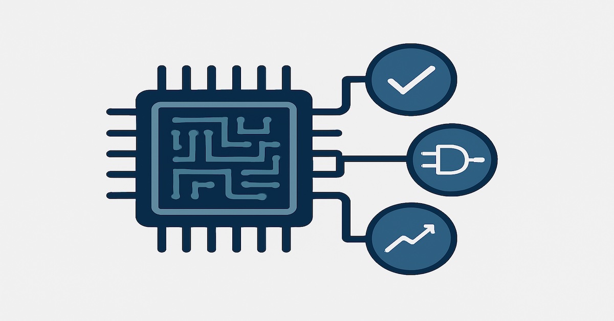
    Image Generated Using 4o


    How DFT Evolved Beyond Test To Impact Reliability

    In the early years of integrated circuit (IC) design, Design-for-Testability (DFT) was primarily introduced to improve manufacturing fault coverage and lower production test costs. Techniques such as scan chains, Built-In Self-Test (BIST), and boundary scans were developed to ensure that devices could be tested efficiently after fabrication. The goal was straightforward: detect manufacturing defects like stuck-at faults or shorts and maximize the number of good parts shipped.

    Reliability, however, existed in a separate part of the development cycle. It focused on burn-in testing, life testing, and field failure analysis; activities typically performed long after the design phase had concluded. Early semiconductor technologies, with larger geometries and lower integration density, were far more tolerant of marginalities, allowing this separation between test and reliability efforts to function without significant consequences.

    However, as the industry pushed into smaller nodes and began designing chips for automotive, medical, and aerospace applications, latent defects and marginal circuit behaviors became much harder to contain. The traditional DFT focus, catching only complex manufacturing faults, was insufficient. Subtle weaknesses introduced during fabrication could evolve into catastrophic failures after months or years of use in harsh real-world environments.

    It became increasingly clear that DFT had to evolve. It was no longer just about passing production tests. It had to become a tool for reliability assurance, enabling early detection of life-limiting defects, supporting real-time health monitoring, and even allowing mechanisms for post-silicon repair.

    From my experience, companies that recognized and embraced this expanded view of DFT, starting in the late 1990s and early 2000s, saw dramatic reductions in field returns and warranty failures, giving them a lasting advantage in high-reliability markets.


    Techniques That Make DFT A Reliability Enabler

    Modern Design-for-Testability (DFT) practices have evolved beyond providing basic test access. Today, DFT intentionally embeds structures and strategies directly contributing to early failure detection, ongoing health monitoring, and long-term reliability assurance. Some of the key techniques that have reshaped DFT’s role include:

    Margin-Aware Testing: Contemporary DFT architectures are designed to detect functional faults and uncover marginal timing vulnerabilities. Techniques such as path delay fault testing, dynamic timing analysis, and voltage and temperature corner testing are now integrated into scan methodologies. These approaches help expose subtle risks like race conditions, timing slippage, and setup/hold margin failures that might otherwise surface only after prolonged field operation or under environmental stress.

    Embedded Health Monitors: Modern ICs now embed a range of on-chip monitors to track critical reliability parameters in real-time. These include thermal sensors, voltage droop detectors, electromigration stress monitors, and aging sensors based on phenomena such as BTI (Bias Temperature Instability) and HCI (Hot Carrier Injection). By continuously observing these degradation mechanisms, the system can identify early warning signs of device wear-out before traditional end-of-life testing catches them.

    Built-In Self-Repair (BISR): While BISR originated in memory arrays to allow the replacement of faulty rows or columns, its philosophy has expanded. Logic BISR concepts are now used to incorporate spare functional blocks, redundant paths, or self-reconfigurable circuits. These enable post-manufacture defect mitigation and even in-field dynamic recovery, which is necessary for high-availability and mission-critical applications like autonomous driving and aerospace systems.

    Accelerated Degradation Detection: Instead of relying solely on lengthy burn-in processes, modern DFT includes stress-inducing scan patterns and high-activity test sequences designed to accelerate latent defect manifestation. Techniques such as elevated voltage toggling, thermal cycling stress patterns, and high-frequency clock strobing allow manufacturers to screen out devices at higher risk of early-life failure during final tests, significantly reducing the “infant mortality” tail in reliability distributions.

    Each technique transforms DFT from a purely manufacturing-oriented tool into a cornerstone of predictive reliability engineering. In my direct experience across multiple technology nodes, products that integrated these advanced DFT capabilities consistently achieved twice the mission life compared to similar designs that treated DFT as a late-stage add-on.

    The lesson is clear: DFT, designed with reliability in mind, becomes a silent but critical insurance policy for every IC leaving the factory.


    Lessons Learned From Real-World Failures

    There is no substitute for experience, especially the hard kind. In the semiconductor industry, field failures often reveal gaps that qualification testing alone cannot uncover. A standard failure mode seen across technologies, particularly in mission-critical applications, involves minor timing shifts and voltage droop effects not captured by nominal-condition scan testing.

    These subtle issues may pass initial qualification yet surface under extreme environmental stresses, such as cold starts or wide voltage variations.

    These cases highlight a critical truth: reliability-driven DFT must extend beyond validating basic functionality. It must be architected to validate timing margins, stress responses, and full-system robustness under real-world operating extremes. Without a margin-aware, environment-sensitive approach, latent vulnerabilities can remain hidden until the device is in the field, leading to costly returns, warranty claims, and potential safety risks.

    Modern best practices now mandate that DFT strategies include corner-aware testing across full environmental ranges, embedded degradation monitors for voltage, temperature, and electromigration, and qualification-resilient test logic that does not become a new failure source itself.

    DFT is no longer viewed as a mere checklist item or manufacturing tool. It is a fundamental mindset shift, treating every test structure and validation point as an active contributor to long-term product reliability and customer trust.


    Best Practices To Align DFT And Reliability

    Specific patterns have become clear after decades of trial and error and technical evolution. Teams that successfully use Design-for-Testability (DFT) to enhance IC reliability follow a deliberate and disciplined approach that starts early, embeds margin awareness, and treats DFT as an investment, not a burden.

    Below is a summary of the best practices that consistently deliver results across complex and mission-critical applications.

    PracticeKey Focus
    Start EarlyIntegrate DFT and reliability engineering during architectural planning, not after layout completion.
    Test Margins, Not Just LogicValidate path delays, power integrity, and signal integrity margins using dedicated DFT hooks.
    Embed Monitors ThoughtfullyPlace thermal sensors, voltage droop detectors, and electromigration monitors strategically at critical locations.
    Plan For In-Field VisibilityArchitect DFT structures that enable monitoring during system operation, not just at manufacturing test.
    Stress Test IntelligentlyUse stress-inducing scan patterns and built-in stress circuits to detect infant mortality risks early.
    Treat DFT As A Reliability AssetShift mindset: view DFT as an insurance policy against field failures and warranty costs, not as overhead.

    As ICs move deeper into critical applications, from autonomous vehicles to implantable medical devices and AI accelerators, the relationship between DFT and reliability will no longer be a luxury or competitive advantage; it will be necessary for survival.

    Those who design with this mindset will not only ship better silicon, they will build trust, longevity, and leadership in industries where failure is not an option.

  • The Use Of AI In Semiconductor Test Program Generation

    Image Generated Using DALL-E


    Semiconductor Testing

    Semiconductor testing, also known as integrated circuit (IC) testing or chip testing, is a critical process in the semiconductor manufacturing cycle. It verifies that ICs function before being deployed in various applications, ranging from consumer electronics to critical automotive systems. This testing phase ensures that only devices meeting the required performance, functionality, and reliability specifications reach the market.

    In a nutshell, semiconductor testing involves applying electrical signals to a chip and measuring the output to assess its performance against predefined criteria. The process is carried out using specialized equipment known as automated test equipment, capable of conducting various electrical tests. Testing can occur at several stages of the semiconductor manufacturing process, including:

    Wafer Testing (Wafer Sort): Test individual chips while still part of the silicon wafer before they are cut out and packaged.

    Package Testing (Final Test): Testing the chips after they have been packaged to check for defects at the final stage.

    Burn-In Testing: Exposing chips to stress conditions (e.g., high temperatures, voltage) to identify early failures.

    The results from semiconductor testing provide valuable feedback to both designers and manufacturers, highlighting potential areas for improvement in chip design and fabrication processes. This feedback loop is crucial for advancing semiconductor technology and increasing yields.


    Test Program And Time Taken

    The development and execution of semiconductor test programs involve several challenges that can significantly extend the time and resources required:

    Complexity: As semiconductor technology advances, chips become more complex, integrating billions of transistors into an ever-smaller area. This complexity makes the test program development more intricate and time-consuming.

    Diverse Test Requirements: Each semiconductor product has unique test requirements based on its application, ranging from consumer electronics to automotive systems. Tailoring test programs to these specific needs adds to the development time.

    High Coverage Requirement: High fault coverage is essential for reliability but requires comprehensive test scenarios and patterns, increasing test time.

    Evolving Standards And Technologies: With continuous advancements in semiconductor technologies and standards, test programs must also evolve, necessitating frequent updates and revisions, which are time-intensive.

    Equipment Utilization: Efficient use of expensive test equipment is crucial. Balancing thorough testing with efficient use of test resources is a constant challenge, as more extensive testing can lead to higher costs and longer test times.

    Given the critical role of semiconductor devices in modern technology, the importance of thorough testing cannot be overstated. It is the final safeguard against defects and failures that could have widespread implications for manufacturers, consumers, and entire industries relying on these components.

    The advancement of testing methodologies, including the integration of AI and machine learning, continues to be a key focus area for improving the efficiency and effectiveness of this crucial process


    Picture By Chetan Arvind Patil

    Using AI In Test Program Generation

    Integrating Artificial Intelligence (AI) into the generation of semiconductor test programs represents a transformative approach to enhancing efficiency, coverage, and speed in the semiconductor manufacturing process.

    The technical integration of AI can be segmented into several key areas, utilizing a variety of AI methodologies including machine learning (ML), deep learning (DL), reinforcement learning (RL), and neural networks.

    A few potential use cases of AI in semiconductor test program generation:

    Automated Test Pattern Generation: AI algorithms can automate the creation of test patterns, significantly reducing the time and expertise required to develop test programs manually. This automation can adapt to the complexity of the semiconductor device, ensuring comprehensive coverage more efficiently.

    Predictive Fault Detection: AI can analyze historical test data to predict potential failure points in new chip designs. This predictive capability allows for targeted testing of high-risk areas, reducing the overall testing time without compromising fault coverage.

    Optimization of Test Sequences: AI can optimize the sequence of test patterns to minimize the test time while maximizing fault coverage. This optimization includes identifying and eliminating redundant tests and prioritizing tests based on their likelihood of uncovering defects.

    Adaptive Testing: AI-enabled test programs can dynamically adjust testing parameters in real-time based on interim results. This adaptability ensures more efficient use of test resources, focusing efforts where they are most needed.

    Learning from Data: AI models improve over time, learning from every test executed. This continuous improvement cycle can lead to increasingly efficient test programs, reducing time and cost with each iteration.

    By leveraging AI, the semiconductor industry can address the significant challenges associated with test program generation.


    Future Course

    The integration of AI in semiconductor test program generation is a transformative approach, leveraging advanced AI techniques to address the complexity and scale of modern semiconductor testing challenges.

    By utilizing AI, the semiconductor industry can address the significant challenges associated with test program generation. AI not only promises to reduce the time and cost associated with testing but also improves the reliability and performance of semiconductor devices, ultimately benefiting manufacturers and consumers alike.


  • The Minor And Critical Semiconductor Test Engineering Differences At Matured And Advanced Node

    The Minor And Critical Semiconductor Test Engineering Differences At Matured And Advanced Node

    Image Generated Using Adobe Firefly


    Semiconductor test engineering is a specialized domain within the semiconductor industry that ensures integrated circuits (ICs) function correctly and meet industry standards before delivery.

    The progression from matured nodes (above 40nm) to advanced nodes (at and below 40nm) has brought about profound changes in the domain of test engineering.

    As an example:

    Coverage: Ensuring complete test coverage becomes challenging as node sizes shrink and transistor counts increase. Test engineers must develop strategies to cover more potential defect sites without increasing test time and, thus, the cost, which is challenging.

    Variations: Advanced nodes are more susceptible to process variations. It emphasizes testing for parametric variations to ensure every chip meets performance and power specifications. It requires collecting quality data during fabrication and ensuring all defective parts get captured during fabrication or testing. All of this adds to the productization cost.

    Defect Mechanisms: As nodes have scaled down, new defect mechanisms related to manufacturing, like random defects and systematic variation, have emerged, requiring new test methodologies. It has increased the cost of capturing these as more sophisticated data and inspection software tools are needed.

    Power: Advanced nodes have power management techniques like multiple power domains, dynamic voltage scaling, and other state machine-driven power requirements. Testing such features requires specialized test patterns and methodologies. Doing so means investing in ATE configurations that can provide the needed setup.

    The dense transistor count on newer nodes made achieving comprehensive test coverage more difficult. Moreover, these advanced nodes have vulnerability to process variations, demanding rigorous testing to ensure consistent performance and power metrics.


    Picture By Chetan Arvind Patil

    The evolution of semiconductor nodes also means complexity in Design for Testability (DFT) has risen, with advanced nodes demanding refined techniques to cater to innovations like 3D stacked ICs and necessitating through-silicon via (TSV) tests. Concurrently, methods such as logic built-in self-test (LBIST) and memory built-in self-test (MBIST) have undergone significant transformations.

    DFT (Design for Testability) Complexity: As nodes have advanced, DFT techniques have become more sophisticated. They are demanding more test hooks to enable coverage.

    Cost Considerations: The cost of testing has been rising, especially for advanced nodes, due to the need to use high-cost ATE systems. It has led to a focus on reducing test times without compromising coverage and adopting more concurrent testing strategies.

    Reliability Testing: With the proliferation of devices in critical applications (e.g., medical, automotive), there is an increased emphasis on testing for reliability, longevity, and resistance to conditions like high temperature and radiation. As more transistors get packed in the smallest area possible, test escapes are always possible, which can lead to quality concerns.

    Data and Machine Learning: With the vast amount of data generated during testing, there is an increased emphasis on using machine learning algorithms to predict defects, optimize test sequences, and improve yield. It is more valid at matured nodes due to the wafer size and the need to develop cost-mitigation techniques to reduce the need to redo a similar process with a test program.

    As the semiconductor industry moved from matured to advanced nodes, test engineering has evolved from focusing on basic functionality checks to a comprehensive discipline that ensures performance, power efficiency, reliability, and safety across intricate designs and multifaceted applications. It invited the problem of cost and time to market and, in many cases, made the productization more complex than ever.

    This story is bound to continue with chiplets, ultra-advanced, and other More-Than-Moore methodologies.


  • The Impact Of Testing In Semiconductor Manufacturing

    The Impact Of Testing In Semiconductor Manufacturing

    Photo by ShareGrid on Unsplash


    Semiconductor testing is one of the most critical steps in ensuring that the product meets all the required specifications and quality standards. Thus semiconductor testing has also become a major driving factor for defect-free products.

    Every chip manufactured has to go through testing processes to ensure the data collected is in line with the expected range. This step ensures the product shipped is fault-free. It requires understanding the product’s internal architecture (by non-designers) before creating testing rules to validate every block within the design.

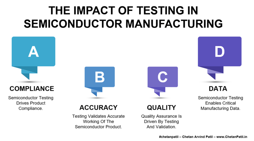
    Compliance: Semiconductor product testing plays a vital role in ensuring the product manufactured meets the compliance targets as per the specification and thus requires testing for the worst to best technical scenarios.

    Accuracy: Semiconductor manufacturing needs to be accurate, and any deviation can impact the production line. Semiconductor testing during the fabrication and post-fabrication stage can reveal whether the product functions accurately or not. It can also provide insights to correct the issues before the product is shipped out.

    Semiconductor testing is also heavily reliant on design techniques. The primary reason is the hooks (non-technical terminology) required to ensure the paths are available to correct test the device. It is where the design for the test strategy comes in to picture.

    As the complexity inside a chip increases, the importance and impact of semiconductor testing will increase too. It also directly impacts semiconductor manufacturing as the goal is always to enable high yield, which is possible only if the testing can reveal the good and the bad parts. It also means thoroughly implementing a full proof and error-free testing process.


    Picture By Chetan Arvind Patil

    In semiconductor manufacturing, there are several stages where testing is needed to collect data.

    The most critical stage is during the fabrication, and testing can reveal if the product is following the correct fabrication process. Any deviation can have a catastrophic effect on the rest of the manufacturing stage. Another critical stage where testing plays a crucial role is the validation stage. This stage can disclose underlying architecture that is not working as expected.

    Quality: Customers are always looking for a product that meets all the quality standards and requirements. Semiconductor testing plays a vital role in ensuring high-quality products. It does so by disclosing any known and unknown issues with the product.

    Data: Only way to know whether a semiconductor product works as expected is by looking at the data, and it is possible only by enabling high volume semiconductor testing.

    Today, one of the hurdles the semiconductor industry faces is the CapEx and resources required for semiconductor testing. An area where the majority of the semiconductor companies find it hard to balance the requirements with the CapEx, and something which will be the primary focus in the years to come. Mainly due to the next era of technology node and package technology.

    Semiconductor testing and the data that comes with it will become more critical for semiconductor manufacturing during the angstrom era. Hence, it will be crucial for the semiconductor equipment and testing teams to innovate solutions that can ensure the complex and advanced products do not lead to escapes. All this while also balancing the time and cost of semiconductor testing.