Category: YIELD

  • The Semiconductor Economics Driven By Yield

    Image Generated Using Nano Banana


    Yield As The Hidden Profit Engine

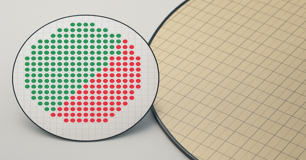
    In the economics of semiconductor products, few variables exert as much influence as yield, yet few receive as little attention outside manufacturing circles. Yield quietly governs how much value can be extracted from every wafer, shaping product cost structures, margin resilience, and overall market viability.

    As devices grow more complex and manufacturing costs continue to escalate, yield increasingly acts as a hidden profit engine, amplifying gains when managed effectively and rapidly eroding profitability when overlooked.

    Yield’s impact is cumulative rather than linear. Small improvements at the wafer, assembly, or test stages compound across high-volume production, translating into meaningful reductions in cost per die and measurable gains in gross margin. From a product perspective, yield directly influences pricing strategy, supply predictability, and return on invested capital.

    Products supported by stable, high-yield manufacturing flows gain critical flexibility, whether to compete aggressively on price or to protect margins in premium markets, shaping economic outcomes long before a product reaches the customer.


    Why Yield Is Economic Leverage. Not Just a Metric

    Yield is often discussed as a manufacturing outcome and viewed primarily as an indicator of process stability, defect control, and operational discipline. While this perspective is technically valid, it significantly understates the yield’s broader economic role. It directly determines how efficiently silicon, capital equipment, energy, and engineering effort are converted into sellable product. As wafer costs rise and device complexity increases, yield becomes one of the most effective levers for influencing product cost without altering design targets or market pricing.

    Unlike many cost-reduction initiatives that require architectural trade-offs or performance compromises, yield improvements compound value throughout the entire production lifecycle. Higher yield increases usable output per wafer, stabilizes manufacturing schedules, and reduces losses from scrap, rework, and late-stage failures. From a product and business standpoint, yield therefore functions as economic leverage rather than a passive metric, shaping profitability, pricing flexibility, and capital efficiency simultaneously.

    DimensionYield Viewed as a MetricYield Viewed as Economic Leverage
    Primary FocusProcess health and defect levelsProduct cost, margin, and profitability
    ScopeIndividual manufacturing stepsEnd to end product economics
    Impact HorizonShort term manufacturing performanceLong term financial and competitive outcomes
    Cost InfluenceIndicates loss but does not control itActively reduces cost per die
    Capital EfficiencyMeasured after investmentGuides investment justification and ROI
    Product StrategyReactive inputProactive decision driver
    Business VisibilityLimited to manufacturing teamsRelevant to product, finance, and leadership

    As semiconductor products move toward advanced nodes, heterogeneous integration, and increasingly complex test and packaging flows, the economic sensitivity to yield will only intensify.

    Companies that elevate yield from a manufacturing statistic to a strategic economic variable will be better positioned to protect margins, sustain innovation, and compete effectively in cost-constrained and performance-driven markets.


    Yield’s Impact On Product Economics

    From a product perspective, yield influences economics at every stage of the lifecycle. During early ramps, unstable yields inflate unit costs and delay break-even points. In high-volume production, sustained yield performance protects gross margins and reduces exposure to cost shocks from scrap, rework, or supply disruptions.

    Products manufactured on mature, high-yield processes gain economic resilience, while those burdened by yield variability often require pricing premiums or volume constraints to remain profitable.

    Economic DimensionRole of YieldProduct Level Impact
    Cost Per DieDetermines usable output per waferLower yield increases unit cost and reduces competitiveness
    Gross MarginExpands sellable volume without increasing wafer startsHigher yield improves margin resilience
    Pricing StrategyEnables flexibility between margin protection and market shareStable yield supports aggressive or premium pricing
    Time to MarketReduces rework and ramp delaysFaster revenue realization
    Capital EfficiencyImproves return on fab and equipment investmentHigher ROI on advanced nodes
    Supply PredictabilityStabilizes output forecastsStronger customer commitments and fewer shortages

    Eventually, yield is not merely a manufacturing outcome. It is a core economic variable that defines how effectively a semiconductor product converts technical capability into financial return.

    Products with strong yield performance gain pricing power, margin stability, and supply reliability, all of which are critical in competitive, cost-sensitive markets.

    As semiconductor products continue to grow in complexity and cost, yield will increasingly determine who wins and loses economically.

    Organizations that integrate yield considerations into product planning, financial modeling, and strategic decision making will be better positioned to deliver profitable, scalable, and resilient semiconductor products.


  • The Semiconductor Yield Management Systems From Data To Intelligence

    Image Generated Using DALL·E


    The Yield Economic Of Semiconductor Manufacturing

    Yield is the percentage of functional chips produced per wafer and is the foundation of semiconductor economics. Every wafer starts as a costly investment in materials, equipment time, and process precision.

    When more dies on that wafer, work perfectly, and each functional chip costs less to produce, margins and profitability improve directly.

    At advanced technology nodes, where wafer costs can exceed tens of thousands of dollars, even a 1% yield gain can translate into millions in savings. This is why yield is not just a technical metric. It is a financial one. High yield lowers cost per die, improves gross margin, and enables companies to price products more competitively.

    As process complexity grows, yield becomes harder to maintain. Each new node introduces tighter tolerances and new failure modes, linking technical precision and financial outcome more closely than ever.

    In essence, yield is the quiet bridge between engineering excellence and economic success and the factor that decides whether innovation becomes profit.

    How Data-Driven Yield Management System Have Evolved

    Yield management has advanced from manual inspection to intelligent, data-driven automation, a transformation shaped by decades of progress in data collection, analytics, and system integration. As semiconductor processes grew more complex, traditional visual checks and spreadsheets could no longer keep pace with the precision required to sustain competitive yields.

    Modern fabs now deploy Yield Management Systems (YMS) that integrate real-time data, advanced analytics, and machine learning to transform yield from a passive metric into a predictive, actionable insight. The table below outlines this evolution:

    EraKey CharacteristicsData CapabilitiesChallenges
    Manual Era
    (1980s–2000s)
    Visual inspections, manual SPC charts, and basic defect tracking.Limited data collection and offline analysis using spreadsheets.Slow feedback loops, poor traceability, reactive response.
    Advanced Era (2000s–2020s)Automated SPC, digital defect logging, and integrated tool monitoring.Centralized data storage with faster trend analysis and limited automation.Limited predictive analytics, partial integration across systems.
    Automated Era (2020s–Present)Real-time data acquisition from MES, metrology, and sensors.Full integration with cloud computing, AI/ML-based yield prediction, and cross-fab traceability.Managing large data volumes, ensuring interpretability of AI results.

    In the early decades, engineers tracked yield using simple control charts and manual logs. These methods provided limited visibility and slow feedback, often revealing problems only after yield had already been lost.

    As wafer complexity increased, manual processes could no longer scale. Semiconductor manufacturers began integrating automated data collection and Statistical Process Control (SPC) into production lines, enabling faster detection of process drifts and systematic analysis of defect trends. This marked the transition from reactive monitoring to structured yield control, where data became central to manufacturing stability.

    FeatureDescriptionPurpose And Impact
    Data Acquisition LayerReal time interface with MES, metrology, and inspection toolsEnables continuous monitoring and instant process feedback
    Statistical Process Control (SPC)Automated Cp Cpk tracking, control charts, and deviation alertsEnsures process stability and early defect detection
    Fault Detection and Classification (FDC)Algorithms identify and categorize process or tool abnormalitiesPrevents downtime by enabling predictive maintenance
    Machine Learning AnalyticsUses PCA, random forests, and anomaly detection for yield predictionDetects subtle variations that impact yield before failure occurs
    Visualization DashboardsUnified display of yield, WAT, and test data across tools and lotsImproves decision speed and cross functional collaboration

    Today, modern fabs operate within a fully connected analytics ecosystem. Yield Management Systems now merge real-time data acquisition, advanced visualization, and machine learning to predict yield excursions before they occur.

    These systems link data from metrology, inline inspection, test, and equipment health monitoring into a unified view, empowering engineers to act proactively rather than retroactively. This evolution has redefined yield from a diagnostic indicator into a strategic, data-driven performance metric.

    Cost, ROI, And The Business Of Yield

    Deploying a Yield Management System involves both technical and financial commitments. Semiconductor manufacturing involves substantial capital costs, including tools, cleanrooms, and data infrastructure.

    Implementing a YMS adds software licensing, integration, and personnel training expenses, but it also transforms how that investment performs.

    By reducing variability, minimizing scrap, and accelerating problem resolution, yield improvements translate directly into lower cost per die and more substantial gross margins. Even a slight percentage increase in yield at advanced nodes can generate multi-million-dollar savings across high-volume production.

    The return on investment extends beyond immediate cost reduction. Higher yields shorten time-to-market, improve equipment utilization, and stabilize supply. These gains compound over a product’s lifecycle, improving financial predictability and enabling greater reinvestment in research and development.

    In essence, a well-implemented Yield Management System becomes not only a quality tool but a profit multiplier, turning data intelligence into sustained economic advantage.

    The Transition From Automation To Intelligence

    Semiconductor yield management is entering a new phase where automation alone is no longer enough. The focus is shifting toward systems that think, learn, and respond in real time. Yield Management Systems are evolving to integrate machine learning, hybrid cloud data platforms, and inline process feedback.

    These advancements allow fabs to identify deviations earlier, make predictive corrections, and maintain consistent output even as manufacturing complexity continues to rise.

    The future of yield management lies in intelligence that is both adaptive and interpretable. Systems will not only detect issues but also understand why they occur and recommend precise corrective actions. This transformation will redefine yield as a measure of insight rather than output.

    In this intelligent era, yield becomes a continuous learning loop, linking every wafer, process, and decision into a unified path of improvement and resilience.


  • The Semiconductor Technical Approach To Defect Pattern Analysis For Yield Enhancement

    Image Generated Using DALL-E


    Semiconductor Defect Pattern Analysis

    The relentless drive for higher performance, lower power consumption, and increased functionality in semiconductor devices has led to unprecedented complexity in semiconductor manufacturing processes. As technology nodes shrink below 3nm and the adoption of 3D structures, such as GAAFETs, becomes widespread, the variability introduced by intricate process steps, material interactions, and equipment behavior poses significant challenges. Traditional yield analysis methods, which primarily rely on statistical summaries and post-mortem evaluations, are no longer sufficient to address these complexities.

    In this evolving landscape, defect pattern analysis has emerged as a methodology for identifying, understanding, and mitigating yield-limiting mechanisms at both macro and micro scales. Defect pattern analysis systematically identifies and characterizes recurring defect trends across wafers, lots, and production lines. Unlike random defects, which occur sporadically and are often isolated, systematic defects are reproducible and stem from persistent issues related to process integration, equipment-induced anomalies, design rule violations, or material inconsistencies.

    These defects manifest in spatial patterns, such as edge-localized clusters, center-focused anomalies, or stepper field-dependent distributions, each offering critical insights into underlying process deficiencies. If not promptly detected and addressed, these defects can significantly degrade electrical performance, reliability metrics, and, ultimately, the economic viability of semiconductor products.

    Understanding Defect Patterns

    Defect patterns in semiconductor manufacturing are intricate signatures that reflect the underlying health of the fabrication process. Analyzing these patterns enables the identification of process anomalies and equipment-related issues that impact yield.

    In semiconductor manufacturing, defects can be broadly categorized into different types based on their occurrence, origin, and distribution. Types of Defects include Random Defects and Systematic Defects. Random defects are sporadic issues that arise due to factors such as contamination, transient process conditions, or environmental disturbances. They are unpredictable and typically isolated. On the other hand, systematic defects are repeatable and consistent, often stemming from process design flaws, equipment malfunctions, or material inconsistencies, making them easier to detect and analyze over time.

    The Sources of Defects are diverse and can occur at various stages of the fabrication process. Lithography Issues, for example, result from misalignment, exposure errors, or anomalies in the photoresist layer, leading to pattern deformation. Etching Variations arise due to over-etching, under-etching, or micro-masking effects, which can compromise feature integrity. Chemical Mechanical Planarization (CMP) Defects are related to issues like dishing, erosion, or irregularities caused by slurry particles, impacting the planarity of wafer surfaces. Additionally, Material Impurities, such as contaminants or non-uniform material deposition, can introduce microscopic defects that affect device performance and reliability.

    When it comes to the Classification of Defects, they are often grouped based on their spatial distribution and recurrence patterns. Clustered Defects are grouped in specific wafer regions, indicating localized process issues that may be tied to equipment or process variations. Repeating Patterns refer to defects that consistently occur in the exact locations across multiple wafers, signaling systematic problems often related to equipment faults or design-related challenges. Edge Exclusions are defects concentrated near wafer edges, typically resulting from process non-uniformities or handling errors during manufacturing. Lastly, Isolated Anomalies are defects that appear randomly across the wafer, usually caused by transient process disruptions or random contamination events.

    Understanding these types, sources, and classifications of defects is critical for effective yield analysis. It enables semiconductor manufacturers to implement targeted corrective actions and improve overall process efficiency.


    Image Credit: A Novel Approach For Wafer Defect Pattern Classification Based On Topological Data Analysis

    Technical Framework For Defect Pattern Analysis

    The technical framework for defect pattern analysis in semiconductor manufacturing is a multi-layered approach designed to capture, process, and interpret defect data systematically. This framework integrates advanced inspection technologies, data acquisition methods, and sophisticated analytical algorithms to identify yield-limiting defects early in manufacturing.

    At the core of this framework is the seamless integration of data from multiple sources. Ranging from in-line process control systems and metrology tools to electrical test results and environmental monitoring. By correlating defect data with process parameters and equipment performance metrics, manufacturers can uncover hidden relationships that might not be evident through traditional analysis methods. This comprehensive approach enhances the ability to detect subtle defect patterns, understand their root causes, and implement real-time corrective actions.

    The following table outlines the key components of the technical framework and details the critical stages involved in defect data management and analysis.

    Data Collection And AcquisitionMapping And VisualizationPattern Recognition And Analysis Process Optimization
    Inspection Tools: Optical and e-beam systems for high-resolution wafer imaging to detect sub-micron defects.Wafer Maps: Graphical displays showing defect locations to identify clusters, edge patterns, and systematic anomalies.Statistical Analysis: Techniques like Pareto analysis and control charts to highlight defect trends and major contributors.Real-Time Feedback Loops: Integration with MES (Manufacturing Execution Systems) for immediate corrective actions.
    Process Data: Equipment logs, process metrics, and environmental data to correlate specific defects with process conditions.Die Maps: Focused mapping of defect distributions within individual dies to identify layout-related and systematic issues.Machine Learning Algorithms: Supervised and unsupervised models for defect clustering, anomaly detection, and predictive analytics.Process Control Adjustments: Dynamic tuning of process parameters based on defect trends to minimize recurrence.
    Test Data: Electrical test results from wafer probing and final test stages to link functional failures with physical defects.Trend Charts: Time-based visualizations tracking defect density trends across production lots and process stages.Root Cause Analysis (RCA): Combining defect data with process knowledge to trace anomalies to specific equipment or process deviations.Preventive Maintenance Scheduling: Using defect trend data to predict equipment failures and proactively schedule maintenance.

    Image Credit: Hitachi

    Importance Of Defect Pattern Analysis In Yield Enhancement

    Defect pattern analysis is pivotal in semiconductor manufacturing, providing critical insights into yield-limiting factors. Its importance lies in detecting, classifying, and mitigating random and systematic defects that directly impact device performance, reliability, and production efficiency.

    By identifying defect trends early in the process, manufacturers can implement targeted corrective actions, minimizing costly rework, material waste, and production delays.

    Furthermore, integrating defect analysis with advanced data analytics and machine learning models enables predictive insights, allowing fans to proactively address potential yield excursions before they escalate into significant issues.

    As semiconductor technologies advance to more complex nodes and architectures, defect pattern analysis becomes even more vital, serving as a strategic tool for continuous process improvement, cost reduction, and maintaining competitive advantage in a fast-evolving global market.


  • The Many Ways In Which Semiconductor Yield Can Be Impacted

    Image Generated Using DALL-E


    Yield, Cost Efficiency And Product Quality

    Understanding the various types of semiconductor yield is essential for optimizing production processes, leading to significant cost savings. Higher yield rates result in more functional chips per wafer, reducing the cost per chip and ensuring efficient use of materials and resources. Manufacturers can minimize waste by identifying and addressing yield-impacting factors, further lowering production costs. This optimization enhances profitability and ensures that the manufacturing process remains sustainable and resource-efficient.

    Yield knowledge also directly correlates with the quality and reliability of semiconductor products. High yield rates ensure that the manufacturing process consistently produces high-quality chips, leading to reliable performance in end-user products. By understanding and mitigating defects, manufacturers can improve their semiconductor devices’ overall quality and reliability. This consistency is crucial for maintaining semiconductor manufacturers’ reputations and meeting the stringent quality requirements of various applications, from consumer electronics to critical infrastructure.

    Yield For Competitive Advantage And Technological Advancement

    Achieving high yield rates is more than just a competitive edge. It is a necessity in the semiconductor market. Companies with optimized yield processes can produce more chips at a lower cost, ensuring they can meet market demand and offer competitive pricing. This advantage is vital in an industry characterized by rapid technological advancements and intense competition. Additionally, leading in yield optimization positions a company as an industry innovator, attracting more business opportunities and potential partnerships, giving you the confidence to compete in this dynamic market.

    A deep understanding of yield types drives continuous improvement in manufacturing processes and the adoption of new technologies. This knowledge is essential for staying ahead in the rapidly evolving semiconductor industry. Manufacturers are encouraged to implement advanced techniques such as Extreme Ultraviolet (EUV) lithography, AI-driven defect detection, and machine learning algorithms by focusing on yield optimization. These advancements improve yield rates and enhance the overall efficiency and capability of semiconductor manufacturing.

    Optimizing semiconductor yield also contributes to better resource management and sustainability. Efficient use of raw materials reduces the need for excessive resources, minimizing environmental impact. Higher yield rates lead to more energy-efficient manufacturing processes crucial for cost savings and ecological sustainability. This approach aligns with global efforts to reduce carbon footprints and promote sustainable industrial practices.


    Picture By Chetan Arvind Patil

    Semiconductor Yield Category And Impact

    In the semiconductor manufacturing industry, yield is a critical metric that measures the efficiency and effectiveness of production processes. Yield refers to the proportion of functional chips produced from a semiconductor wafer. Understanding the various categories and factors that impact semiconductor yield is essential for optimizing production, reducing costs, and maintaining high product quality. This section will explore critical factors influencing semiconductor yield, ranging from defect density and process variability to advanced technological practices and future trends.

    Category and Impact FactorDescription
    Defect Density and ControlDefect density refers to the number of defects per unit area on a wafer, which can cause chips to be unusable.
    Process VariabilityVariations in temperature, pressure, and chemical concentrations during manufacturing can affect yield.
    Equipment Reliability and MaintenanceInconsistencies in machine performance, malfunctions, and wear and tear can disrupt the manufacturing process.
    Material Quality and PurityVariations in the quality and purity of raw materials, such as silicon wafers, can introduce defects.
    Human Factors and TrainingHuman errors and differences in operator skills can impact yield.
    Environmental ControlEnvironmental factors like cleanroom standards, humidity, and vibration control affect yield.
    Design for Manufacturability (DFM)DFM ensures products are designed with the manufacturing process in mind to enhance yield.
    Advanced Lithography TechniquesLithography involves using light to transfer patterns onto the wafer, where variations can cause defects.
    Statistical Process Control (SPC)SPC tools help monitor and control process variations to improve yield.
    Yield Management Software and AnalyticsAdvanced software and data analytics are used to identify and address yield issues.
    Future Trends in Yield EnhancementEmerging trends such as AI, machine learning, and new materials promise future yield improvements.

    Understanding the numerous factors that impact semiconductor yield is vital for any organization aiming to excel in the semiconductor industry. Manufacturers can significantly enhance yield rates by addressing issues such as defect density, process variability, equipment reliability, and material quality. Additionally, embracing advanced technologies and innovative practices will pave the way for future improvements in yield. By focusing on these critical areas, companies can achieve higher efficiency, reduced costs, and superior product quality, ultimately maintaining a competitive edge in the rapidly evolving semiconductor market.

    How Will AI Impact Yield Detection And Improvement

    As I conclude this exploration of the factors impacting semiconductor yield, one must highlight the transformative role of Artificial Intelligence (AI) in yield detection and improvement. AI is poised to revolutionize semiconductor manufacturing, providing advanced capabilities to enhance yield rates significantly.

    Enhanced Defect Detection: AI-driven systems are highly efficient in identifying defects, surpassing traditional methods in accuracy and speed. Machine learning algorithms can sift through vast amounts of data from production processes to spot patterns and anomalies that may indicate defects. This real-time analysis enables immediate corrective actions, thereby reducing the number of defective chips and enhancing overall yield, providing a sense of reassurance about the quality of the products.

    Predictive Maintenance: AI’s predictive capabilities can foresee equipment failures by analyzing data from sensors and maintenance logs before they occur. This proactive approach ensures that machinery operates at optimal performance levels, minimizing downtime and preventing defects caused by equipment malfunctions. Such proactive measures instill a sense of security about the reliability of the equipment and the stability of the manufacturing environment, which is crucial for high yield.

    Process Optimization: AI algorithms are crucial in continuously monitoring and adjusting manufacturing processes to maintain optimal conditions. By analyzing data from various stages of production, AI can identify process variations and recommend adjustments to maintain consistency. This dynamic process control helps reduce variability, ensuring that each wafer meets the required standards for high yield.

    Quality Control: AI enhances quality control by providing precise and consistent inspections. Automated visual inspection systems powered by AI can identify even the most minor defects that human inspectors might miss. This increased accuracy ensures that only high-quality chips progress through manufacturing, improving the overall yield.

    Big Data Analytics: AI leverages big data analytics to provide insights into yield trends and potential issues. By aggregating and analyzing data from multiple production lines and facilities, AI can identify systemic problems and recommend solutions. This holistic view of the manufacturing process helps manufacturers implement best practices and continuously improve yield rates.

    Take Away

    Understanding the myriad factors that impact semiconductor yield is essential for optimizing production, reducing costs, and maintaining high product quality. Manufacturers can significantly enhance yield rates by addressing defect density, process variability, equipment reliability, and material quality issues. Embracing advanced technologies like AI and machine learning improves yield detection and defect management and drives continuous process optimization.

    These innovations lead to higher accuracy in defect detection, proactive maintenance, and better quality control, ultimately resulting in more efficient and sustainable manufacturing practices. As the semiconductor industry continues to evolve, focusing on yield improvement will be vital to maintaining a competitive edge and meeting the growing demand for reliable, high-quality semiconductor products.


  • The Economic Implications Of Semiconductor Yield From A Product Perspective

    Image Generated Using DALL-E


    Importance Of Semiconductor Yield

    Semiconductor yield, the percentage of functional chips produced from a wafer, is a critical factor in the semiconductor industry. Yield influences production’s cost efficiency and determines manufacturing operations’ overall economic viability.

    High yield directly impacts various economic aspects, including cost per chip, profit margins, market competitiveness, investment in technology, and supply chain efficiency.

    Let us explore these implications from a product perspective, providing a comprehensive understanding of how yield affects the broader semiconductor landscape.


    Key Metrics For Semiconductor Yield Analysis

    As a first step, yield analysis involves understanding the percentage of functional chips produced from a wafer and identifying the factors influencing this outcome. By leveraging key metrics, manufacturers can gain insights into their production processes’ effectiveness, identify improvement areas, and make informed decisions to enhance yield performance.

    This analysis improves the technical aspects of manufacturing and has profound financial implications, impacting profitability, cost management, and overall competitiveness. This section delves into the essential metrics used in semiconductor yield analysis, explaining their definitions, importance, and practical applications.

    Die Yield: Die yield is the percentage of functional dies (chips) on a wafer. It measures the effectiveness of the manufacturing process. A high die yield indicates fewer defects and greater efficiency, leading to lower costs and higher profitability.

    Defect Density (D0): Defect density is the number of defects per unit area on the wafer. Lower defect density indicates a cleaner manufacturing process and higher yield potential. It is an essential metric for assessing the quality of the production environment and processes.

    Overall Yield: Overall yield considers multiple manufacturing stages and their yields. This metric provides a comprehensive view of the entire production process’s effectiveness. It highlights the importance of optimizing each stage to achieve a high yield, ensuring consistent and efficient production.

    First-Pass Yield (FPY): Measures the percentage of products that pass all manufacturing stages without rework or repair. It is an indicator of process efficiency and quality. A high FPY reflects a well-optimized manufacturing process with minimal defects and interruptions, reducing production costs and faster time to market. Monitoring FPY helps identify areas in the production process that may need improvement to enhance overall yield and product quality.

    Yield Model: Murphy’s model predicts yield based on defect density and die area. This model helps understand the relationship between defect density and yield, which helps make informed decisions about process improvements and defect reduction strategies.

    Gross Die Per Wafer (GDW): Gross die per wafer is the total number of dies that can be produced from a single wafer. This metric helps estimate the potential production volume based on the wafer’s diameter and the area of a single die. It is crucial for planning manufacturing capacity and understanding production limits.

    Critical Area Analysis: Critical area analysis estimates the yield loss due to defects in specific die areas. Manufacturers can target improvements more effectively by identifying and addressing critical areas where defects can cause failures. This analysis is vital for optimizing design and manufacturing processes to enhance yield.

    Return On Investment (ROI): Measures the profitability of an investment relative to its cost. In semiconductor manufacturing, ROI is calculated for investments in new technology, equipment, or process improvements. A higher ROI indicates that the investment has generated significant returns, justifying the expenditure.

    Gross Margin: Gross margin is the difference between revenue and the cost of goods sold (COGS), expressed as a percentage of revenue. It indicates the efficiency of the manufacturing process and the product’s profitability. Higher gross margins reflect better cost control and higher profitability.

    Yield To Cost (YTC): Measures the relationship between yield improvements and cost reductions. It assesses how changes in yield affect overall production costs. A positive YTC indicates that yield improvements effectively reduce costs and enhance profitability.

    Cost Per Die: Total manufacturing cost divided by the number of functional dies produced. This metric helps understand the cost efficiency of the manufacturing process. Lower CPD indicates higher efficiency and better cost management.

    Break-Even Yield: The yield percentage of total revenue equals total production costs, resulting in neither profit nor loss. Understanding BEY is crucial for setting yield targets that ensure profitability. Achieving yields above BEY ensures that the manufacturing process is profitable.


    Picture By Chetan Arvind Patil

    Economic Implications Table

    To fully grasp the economic implications of semiconductor yield, analyzing how yield improvements influence different aspects of semiconductor production and their subsequent effects on the market is essential. The table below highlights the primary areas affected by yield and provides examples to illustrate these impacts:

    AspectDetailsImplication
    Cost Per ChipReduces manufacturing costs by lowering per-unit cost through higher yield. Achieves economies of scale, enabling competitive pricing.A 1% yield improvement can save millions for smartphone manufacturers.
    Profit MarginsEnhances profitability by increasing the number of sellable units per wafer. Improves gross margins, supporting financial stability.Minor yield improvements can significantly boost profits in high-value processors.
    Market CompetitivenessBalances price and performance, attracting cost-conscious consumers. Ensures performance consistency, differentiating in premium segments.High yields allow consumer electronics brands to deliver high-performance, competitively-priced devices.
    Investment In TechnologyJustifies significant RnD investments, driving innovation. Ensures sustainable growth by maintaining high yields.Investments in advanced technologies support high yields and industry leadership.
    Supply Chain EfficiencyLeads to predictable production outputs, facilitating better planning. Optimizes inventory, reducing excess stock and avoiding shortages.High yield ensures a steady supply of chips, crucial for just-in-time production models.

    As demonstrated in the above table, each aspect of semiconductor yield significantly impacts the economic dynamics of semiconductor manufacturing. High yield is a crucial driver of financial success in the industry, from reducing the cost per chip to enhancing supply chain efficiency.


    Importance of Modeling in Semiconductor Yield Analysis

    Modeling provides a framework for predicting, analyzing, and optimizing yield, offering significant advantages in various aspects of semiconductor manufacturing. The table below focuses on the critical benefits of modeling in yield analysis and includes illustrative examples and case studies.

    By leveraging advanced modeling techniques, semiconductor manufacturers can significantly enhance their yield performance, driving economic success and maintaining market competitiveness.

    AspectDetailsImpact
    Accurate Yield PredictionsPredicts yield outcomes based on process parameters and defect rates, aiding in informed decision-making.Using statistical models to estimate yield in wafer production improves forecasting accuracy.
    Process OptimizationSimulates different process conditions to identify optimal settings that maximize yield and minimize defects.Modeling optimal etching parameters in semiconductor fabrication to enhance yield.
    Defect Analysis And MitigationUnderstands the relationship between defects and yield loss, enabling targeted defect mitigation strategies.Analysis of critical defects in photolithography processes, leading to improved cleanroom protocols.
    Cost ReductionIdentifies yield-limiting factors early, avoiding costly rework, scrap, and downtime, thus reducing production costs.Early detection of yield issues in chip packaging, saving costs associated with rework and scrap.
    Innovation And DevelopmentProvides a virtual testing ground for new technologies and processes, accelerating the development cycle.Simulation of new materials in transistor design, reducing time-to-market for advanced technologies.
    Risk ManagementAssesses potential risks of yield fluctuations and develops contingency plans to ensure stable production outputs.Risk assessment models for managing yield variability in high-volume semiconductor manufacturing.
    Continuous ImprovementRegularly updates models with new data to refine yield dynamics understanding, driving higher performance over time.Ongoing improvement in yield prediction models for dynamic random-access memory (DRAM) production.
    Predictive ModelingForecasts yield outcomes based on wafer inspection data, allowing for preemptive corrective actions.Use of machine learning algorithms in memory chip production to predict and mitigate yield issues.


    Take Away

    The economic implications of semiconductor yield are profound, affecting cost per chip, profit margins, market competitiveness, investment in technology, and supply chain efficiency. High yield is essential for maintaining competitive pricing, enhancing profitability, driving innovation, and ensuring supply chain stability.

    As technology advances, semiconductor manufacturers will continue to prioritize higher yields. Ongoing improvements in manufacturing processes, defect detection, and technological innovation will drive the industry’s growth and economic viability, ensuring that semiconductor yield remains a critical determinant of success.


  • The Importance Of Yield In Validation Of New Semiconductor Products

    Image Generated Using DALL-E


    Semiconductor Product Development And Yield Correlation

    The semiconductor industry continually innovates and introduces new products to meet the growing demands for more powerful and efficient electronic devices. The successful launch of these new semiconductor products always hinges critically on yield.

    As such, yields are not just a statistic in semiconductor terminology. They impact the production costs per usable chip, which can significantly affect profit margins, particularly in a highly competitive market with limited pricing power.

    From A Semiconductor Product Perspective: Yield is considered after the chip has been fabricated, assembled, and tested. It involves the proportion of chips that function correctly and meet the desired performance specifications. This aspect of yield is crucial because it determines the compliance, quality, and eventually the profitability of the new semiconductor product.

    Moreover, the correlation between yield and the broader semiconductor industry extends to how companies manage their supply chains and respond to market demands. Thus, a stable and high yield is crucial for maintaining reliable product supply, affecting market share and consumer confidence.

    Eventually, effective yield management will support cost efficiency, product quality, strategic positioning, and competitive advantage in the semiconductor landscape.


    Setting And Achieving The Target Yield

    Setting the target yield in semiconductor product development is a critical strategic decision that balances technical feasibility with business goals. Companies often set this target based on historical yield data, technology (node) used, product complexity, and defectivity to anticipate and mitigate potential production to cost challenges.

    “What Is Target Yield? Refers to the predefined goal for the percentage of functional units produced from a batch of semiconductor wafers. Semiconductor companies set a target yield to measure the efficiency and effectiveness of their products and processes. Setting a target yield is vital for several reasons, including cost control, production planning, and ensuring the economic viability of manufacturing operations.”

    On other hand, achieving yield targets is a multifaceted process that involves a series of detailed and strategic testing stages. Each stage addresses different aspects of a semiconductor’s functionality and performance, progressively ensuring that yield targets are verified and, if not met, then the product is improved through another silicon revision by root causing the issue.

    Below are the different testing methods that are used to validate the semiconductor product and the yield:

    StageDescriptionImpact on Yield
    Simulation-Based TestingUtilizes advanced computational models to predict how a semiconductor device will behave under various physical, electrical, and environmental conditions before actual physical testing begins. It helps identify potential issues before they manifest in real-world scenarios.It improves yield by enabling early detection of design flaws and operational shortcomings, reducing the need for costly physical reiterations.
    Bench TestingInitial assessment of each chip under controlled conditions to verify it meets fundamental design specifications.Lays the groundwork for higher yield rates by identifying and correcting early design discrepancies.
    Application TestingTests the chip within its specific intended application (e.g. a computer processor) to evaluate performance in operational environments.Boosts yield by refining design and manufacturing processes to reduce application-specific failures.
    System-Level TestingIntegrates the chip with other hardware and software to ensure compatibility and meeting performance metrics across a system.It is identifying integration issues that might affect yield, such as electric interference and data throughput issues.
    Assembly/PackagingIt involves encapsulating the die in a protective casing and testing for physical, thermal, and chemical resilience.Ensures mechanical and environmental robustness, directly influencing yield concerning product longevity and failure rates.
    Test/Automatic Test Equipment (ATE)Simulates real-world operating conditions to test the chips for quality and durability rigorously.Minimizes late-stage production failures, achieving high yield by ensuring readiness and reliability under operational specifications.
    Quality ControlTesting all manufacturing process aspects to adhere to stringent quality standards.Maintains high yield rates by ensuring consistent quality across production batches and over time.
    Reliability TestingFocuses on the long-term performance of the chips, predicting and improving life expectancy and failure rates.Enhances yield rates by identifying late-life failures, which is crucial for customer satisfaction.

    Picture By Chetan Arvind Patil

    Yield And COGS

    In the semiconductor industry, the Cost of Goods Sold (COGS) encompasses various elements such as fabrication, assembly, testing, material costs, direct labor costs, and other overheads. However, the one factor that truly holds the power to influence the product margin, driven by COGS, is yield. Thus, reduction or increasing in the number of good products per wafer (i.e.  yield) impacts manufacturing costs (COGS), making it a crucial aspect to consider.

    Below is a view of how achieving a target yield helps with lower COGS and the production of a product:

    Impact On COGS: Improved yields directly lead to lower COGS as the effective utilization of inputs (materials, labor, and capital) increases. It is crucial in the semiconductor industry, where price erosion is common, and the ability to rapidly reduce costs can be a significant competitive advantage.

    Pricing Flexibility: Lower COGS allows greater flexibility in pricing its products. It can be critical in competitive markets or when companies seek to penetrate new markets by underpricing competitors without sacrificing margins.

    Profitability: Lower COGS resulting from higher yields boosts gross margins, a key indicator of production efficiency and profitability. In a capital-intensive industry like semiconductors, where initial investments and fixed costs are high, maximizing yield is often synonymous with maximizing profitability.

    Inventory Management: Higher yields can lead to more consistent production outputs, which helps better inventory management. Companies can reduce the buffer stocks they might otherwise hold to compensate for potential yield variability, thus minimizing the costs associated with holding inventory.

    Eventually, companies that excel in yield optimization improve their operational efficiencies and strengthen their financial (where COGS is crucial) position, providing more stability in the volatile semiconductor market.


    Semiconductor Yield Take Away

    By now, it is obvious how important the yield is in validating new semiconductor products. Yield also influences several aspects of a semiconductor company’s operations, from financial stability to market competitiveness.

    To summarize, here are four key takeaways on how crucial yield is during the validation phase of new semiconductor products:

    • Cost Efficiency And Profitability:
      • Yield directly impacts the cost efficiency of semiconductor manufacturing. Higher yields mean more functional devices are produced per batch, reducing the per-unit cost of production. This cost-saving is crucial when scaling up production for market launch.
      • Effective yield management during the validation phase can dramatically enhance profitability by minimizing waste and optimizing resource use, setting a solid foundation for competitive pricing and healthy profit margins as the product enters the market.
    • Product Quality Add Reputation: 
      • Achieving a high yield is synonymous with ensuring product quality during validation. High yield indicates that the manufacturing processes can consistently produce devices that meet or exceed specifications.
      • This strengthens customer trust and satisfaction and enhances the product’s reputation for reliability. A high yield during product validation can thus serve as a quality assurance marker, reassuring stakeholders and customers about the product’s performance and durability.
    • Time To Market And Competitive Advantage: 
      • Yield optimization during validation affects a company’s agility and speed in bringing new products to market. High yield rates allow for a smoother transition from development to full-scale production, reducing delays caused by extensive troubleshooting and reiterations.
      • This speed to market is a crucial competitive advantage, especially in a fast-paced industry like semiconductors, where being first can dictate market leadership and capture significant market share.
    • Supply Chain Stability And Responsiveness: 
      • High yields during the validation phase contribute to supply chain stability by ensuring production volumes meet forecasted demands. This stability is crucial for maintaining consistent customer supply and responding flexibly to market demand changes. 
      • Moreover, predictable and stable yields reduce the risk of stockouts and excess inventory, thus optimizing the supply chain operations and reducing logistical costs.

    In conclusion, yield must be considered critical when designing, manufacturing, and validating new semiconductor products. More so, when yield touches every essential aspect of a semiconductor company’s operations – from cost structure and product quality to market positioning and supply chain management.

    In the long term, effective yield management during product validation is a strategic imperative that underpins operational efficiency and the long-term success of a product in the semiconductor industry.


  • The Wafer Excursions And Impact On Semiconductor Yield

    Image Generated Using DALL-E


    Yield And Wafer Excursions:

    In the complex world of semiconductor manufacturing, maintaining a high yield – the percentage of functional devices from a batch of wafers – is the ultimate goal. However, various challenges, including wafer excursions, can impede this process.

    These wafer-level deviations from the standard processing environment often impact yield by introducing defects that affect the final product’s performance and reliability. Thus, in addition to several yield-related learnings, it is also crucial to understand wafer excursions and how they correlate to introducing new semiconductor products.

    Premier On Wafer Excursions:

    Wafer excursions refer to any anomalies that occur during the semiconductor manufacturing process, deviating from the controlled conditions expected in production. 

    These can range from several fluctuations in material, mask, fabrication step, equipment, etc. The consequences of these excursions can be severe, creating defective chips that fail to meet the required specifications. Thus, they impact customer satisfaction (from a process point of view) and raise concerns about product quality.

    Type Of Wafer Excursions:

    The key to managing wafer excursions lies in their precise identification and categorization. Each type, with its distinct causes and effects, requires this level of detail. It is through this process that we can ensure the correct preventive measures and responses are implemented.

    There are four main categories of wafer excursions based on their origin and nature.

    Type of ExcursionDescription
    Process ExcursionsDeviations in processing parameters such as temperature, pressure, chemical concentration, or deposition rates. For example, over-etching leading to faulty circuits.
    Equipment-Related ExcursionsFaults or malfunctions in manufacturing equipment like lithography tools, etchers, or deposition systems that lead to inconsistent processing across the wafer.
    Environmental ExcursionsVariations in the cleanroom environment, such as changes in temperature, humidity, or particulate contamination, which can adversely affect the processes.
    Material ExcursionsIssues with the materials used in the process, such as contamination, incorrect mixing, or improper handling of dopants, metals, or gases.

    Understanding these excursions is crucial for setting up effective monitoring systems, developing robust manufacturing protocols, and training personnel to handle and respond to potential deviations promptly.

    With this knowledge, manufacturers can significantly enhance their ability to maintain high yields and produce reliable, high-quality semiconductor products.


    Picture By Chetan Arvind Patil

    Detecting The Wafer Excursions:

    Advanced detection technologies are vital in identifying deviations from standard manufacturing processes early in the production cycle. These technologies enable manufacturers to intervene promptly, correcting issues before they escalate into significant yield losses.

    Here is a comprehensive table outlining the various detection techniques used in semiconductor manufacturing to identify and address wafer excursions:

    Detection MethodTechnology and Application
    Inline DataTools that measure critical dimensions, film thicknesses, and other physical to die level characteristics of wafers during manufacturing. These real-time measurements help in detecting deviations promptly.
    Defect Inspection SystemsUtilize various imaging techniques, such as optical or electron microscopy, to identify physical defects on the wafer surface. Capable of detecting particulate contamination, pattern anomalies, and other defect types.
    Electrical TestingConducted at various stages of the manufacturing process to assess the electrical functionality of circuits. This testing helps identify electrical failures that might indicate underlying physical or process defects.
    Environmental MonitoringSensors continuously monitor the cleanroom environment for particulates, chemical vapors, temperature, and humidity, providing alerts to any conditions that could destabilize the process.

    Integrating advanced detection techniques into semiconductor manufacturing processes is crucial for minimizing the impact of wafer excursions. These technologies enhance the ability to detect and correct deviations quickly and contribute to the overall efficiency and cost-effectiveness of semiconductor manufacturing.

    These detection methods will evolve as technology advances, offering even greater precision and reliability in monitoring manufacturing processes.

    Impact of Wafer Excursions:

    The impacts of excursions are far-reaching, affecting yield and the long-term reliability of semiconductor devices. It is imperative that manufacturers understand these impacts and implement effective strategies to mitigate risks and enhance product quality.

    The table below captures the primary impacts of wafer excursions on semiconductor manufacturing. 

    Impact CategoryDescription
    Yield ReductionSmall deviations in the manufacturing process, especially in critical stages like photolithography, can lead to significant yield losses.
    Reliability IssuesExcursions can introduce latent defects into devices, which may not cause immediate failures but can decrease the devices’ long-term reliability.
    Scrap and ReworkIn severe cases, excursions can necessitate the scrapping of entire batches of wafers or require costly rework to salvage usable components.

    These disruptions can have serious consequences, from reduced yield and reliability to increased costs due to scrap and rework. For semiconductor manufacturers, quickly detecting and effectively responding to wafer excursions is not just a technical necessity. 

    It is a critical business strategy that directly impacts profitability and market competitiveness.

    Preventive, Corrective Actions And Take Aways For Wafer Excursions:

    In the field of semiconductor manufacturing, precision and reliability are of utmost importance. To ensure efficient production, it is essential to implement robust preventive strategies.

    These strategies are designed to minimize the occurrence of wafer excursions by addressing potential issues before they impact the production process. Below is a table outlining the key preventive measures.

    StrategyDescription
    Process Control EnhancementsAdvanced Process Control (APC) systems utilize real-time data from inline metrology to automatically adjust process parameters, ensuring stable and controlled manufacturing conditions.
    Predictive MaintenanceThis approach uses data analytics to predict potential equipment failures before they occur, thereby reducing the risk of equipment-related excursions.
    Improved Material Handling ProtocolsStrict protocols ensure that all materials are handled, stored, and used under controlled conditions to prevent contamination or degradation, maintaining the integrity of the manufacturing process.

    Companies invest heavily in preventive strategies to safeguard the integrity of semiconductor manufacturing processes. These strategies are designed not only to detect and correct wafer excursions but also to prevent their occurrence. By implementing advanced systems and protocols, manufacturers can maintain a high level of process control and material integrity, which are crucial for minimizing disruptions and ensuring consistent product quality.

    To conclude, wafer excursions pose significant challenges in the semiconductor manufacturing, affecting everything from yield to device reliability. Through a comprehensive understanding of the types and impacts of these excursions, coupled with advanced detection techniques and robust preventive strategies, manufacturers can effectively manage and mitigate their effects.

    The proactive management of wafer excursions is not just about enhancing yield, but about ensuring the production of high-quality, reliable semiconductor devices. This holistic management, which is the key to maintaining the operational efficiency and economic viability of semiconductor manufacturing in an increasingly demanding and competitive market, puts the control back in the hands of manufacturers.


  • The Economics Of Semiconductor Yield

    Image Generated Using DALL-E


    The semiconductor industry is driven not just by innovation but also by the economics of production. At the core of this economic landscape is yield – a term that might seem technical at first glance but also drives the financial realities of semiconductor manufacturing.

    Understanding this economic aspects of semiconductor yield offers insights into how this industry balances the scales of cost, quality, and supply. Below are a few critical points to showcase how yield impacts semiconductor product development and the mass production phase.

    Cost:

    Yield is the percentage of functional devices on a silicon wafer. The yield rate is a pivotal factor in an industry where production costs are sky-high. High yields translate to more usable chips per wafer, reducing the cost per chip.

    It is particularly relevant given the fixed and substantial costs of setting up and running semiconductor fabrication plants (FABs). Low yields, on the other hand, spike up the cost per functional chip, impacting business.

    Quality:

    Achieving and maintaining high yields necessitates substantial investments in quality control and process optimization. While demanding in the short term, these investments can yield long-term economic benefits.

    Enhanced quality control measures lead to fewer defects, higher yields, and, thus, better returns on investment. This continuous cycle of investment and improvement is a hallmark of the semiconductor industry’s commitment to economic efficiency.

    Pricing:

    Yield rates also have a direct bearing on how companies price their products. In a market where competition is fierce, the ability to offer competitive pricing hinges on yield efficiency.

    High yields allow for more aggressive pricing strategies, while lower yields might compel companies to hike prices to maintain profitability.


    Picture By Chetan Arvind Patil

    RnD:

    The relentless pursuit of higher yields is a significant driver of research and development (RnD) in the semiconductor sector. RnD efforts to enhance yields involve more than incremental improvements in existing processes.

    But also groundbreaking work in new manufacturing technologies and materials. This aspect of yield economics represents a substantial portion of the industry’s investment in future capabilities.

    Supply And Demand:

    Yield rates are not just about cost efficiency. They also play a crucial role in determining the supply of chips in the market. In times of surging demand, such as during technological booms or shortages, the ability to produce high yields can be economically game-changing.

    Conversely, low yields can exacerbate supply shortages, leading to market imbalances.

    Advanced Nodes:

    The semiconductor industry is adopting ultra-advanced technology nodes (smaller feature sizes). The challenge of maintaining high yields becomes even more pronounced.

    The economic stakes are higher in these advanced nodes, where the cost of defects and low yields can be significantly more impactful.

    In conclusion, the journey through the economics of semiconductor yield unveils complicated factors that drive one of the most technologically advanced industries in the world. Yield is not just a measure of production efficiency. It is a crucial economic lever that shapes pricing strategies, drives technological innovation, and dictates market supply and demand.

    As the semiconductor industry continues to evolve amidst rapidly changing technological landscapes and shifting market demands, understanding and optimizing yield remains a key to unlocking economic success and sustainability. This exploration underscores the profound impact that a seemingly technical metric can have on the broader economic and environmental landscape of semiconductor manufacturing. Thus also opening avenues for future students and professionals to learn and explore careers around them.


  • The Ever-Growing Need For Semiconductor Yield Management

    Image Generated Using Adobe Firefly


    The manufacturing of semiconductor devices is a highly intricate process that involves multiple steps. Even minor deviations in these steps can result in defects that render the device non-functional. Semiconductor yield management is a process that aims to identify and address yield issues to ensure that the devices produced are of the desired quality and functionality. Its main goal is to maximize yield by minimizing the number of defective devices and optimizing the manufacturing process for better productivity.

    Often, yield management is assumed to be only about silicon test data. In reality, it is much more than that. It is about ensuring all the process steps from wafer start-up until the final packing stage is equipped with a yield monitoring process

    Semiconductor yield management requires specialized tools and software to monitor, analyze, and optimize the production process. These also need trained talents to use and make the most of the data presented.

    As an example, defect inspection tools help to scan wafers at various stages of the process steps. It allows the detection of physical defects. Similarly, Scanning Electron Microscopes (SEMs) provide high-resolution imaging to detect and analyze weaknesses that are not possible due to defect inspection tools – mainly as part of failure analysis.

    At the testing stages, a flawless yield management software that can work synchronously with Automated Test Equipment (ATE) to capture, process, and analyze vast amounts of data is needed. This end-to-end data is crucial in ensuring the yield out of the wafer is in line with the specification, and YMS tools offer various features to facilitate the review process that may arise due to any excursions or issues during testing.

    In line with YMS, there is Statistical Process Control (SPC) Software, too, that ensures in real-time, the process remains within specified limits. On top of that, many of the SPC tools have different types of rules that can capture test-driven deviations in real during silicon wafer testing.


    Picture By Chetan Arvind Patil

    Semiconductor yield management is a multifaceted domain that combines technical expertise with analytical and interpersonal skills. Some of the top-level skills a talent needs to have are:

    Analytics: Yield management is analyzing large amounts of data to identify patterns, anomalies, and potential causes of defects. Professionals in this field must be skilled in dissecting data, using statistical tools, and deriving actionable insights from complex datasets. Additionally, having the ability to write automated tools in various programming languages is an added advantage.

    Focus: Manufacturing semiconductors involves thousands of intricate steps, and even the slightest deviation can lead to defects. It is essential to possess a keen eye for detail to identify and rectify minute discrepancies that others might overlook. Additionally, understanding different sets of fabrication process steps and how to connect the anomalies is also crucial for ensuring a successful outcome.

    Problem-Solving: Yield management professionals must quickly diagnose and resolve issues during the production process, using a structured approach to creative problem-solving.

    Communication: Interdisciplinary teams of yield management professionals must communicate effectively to relay findings, suggest improvements, and ensure corrective measures are implemented. It is like a decision review system (as in Cricket), where the solution goes through a review before it gets deployed.

    Collaboration: Yield improvement is a collective effort. Collaboration among professionals from various functions is crucial for yield improvement.

    Decision: With the vast data, yield management professionals must make timely and informed decisions, balancing the trade-offs between quality, cost, and production speed.

    Traditionally, the semiconductor end-to-end data analysis is not only challenging to capture (due to disaggregated tools and equipment) but is also costly. The costly aspect is due to the need to deploy a proper set of hardware and software systems that can provide end-to-end data capturing.

    So far, many yield management flows in the semiconductor industry have yet to adopt the cloud and AI strategy. And, with AI usage increasing, it has become crucial for semiconductor companies to not only embrace AI solutions but also move or adopt cloud solutions to ensure the AI features can be developed at scale, as both go hand in hand.

    Cloud: With the increasing complexity of semiconductor designs and processes, the amount of data generated during manufacturing has grown exponentially. Cloud platforms offer vast storage capabilities and enable seamless access to data across global manufacturing sites. This centralization facilitates real-time data analysis and quicker decision-making. Semiconductor engineers and data scientists from different locations can simultaneously analyze data, discuss findings, and implement solutions, ensuring that yield optimization strategies are consistent across facilities.

    Art Of AI: AI algorithms can predict potential yield issues based on historical data. This proactive approach allows manufacturers to address potential problems before they manifest, ensuring higher yields. Traditional methods can be time-consuming. AI can quickly sift through vast datasets to pinpoint the root causes of defects, accelerating the troubleshooting process.

    Hurdles: Transitioning to the cloud brings concerns about data security and intellectual property protection. Semiconductor firms need robust security protocols to prevent breaches. Integrating cloud and AI solutions with existing infrastructure and workflows can be complex.

    Future: The fusion of cloud computing and AI in semiconductor yield management promises a future of higher yields, reduced production costs, and faster time-to-market. As these technologies mature and the industry overcomes the initial hurdles, one can expect a more streamlined, efficient, and responsive semiconductor manufacturing landscape. The focus will shift from reactive problem-solving to proactive yield optimization, ushering in a new era of semiconductor production excellence.

    Semiconductor yield management has evolved from manual inspections and rudimentary data analysis in the past to sophisticated real-time monitoring and advanced analytics in the present.

    As the semiconductor industry looks to the future, integrating cloud computing and AI promises unprecedented optimization, driving yields to new heights and redefining industry standards.